

Page 1
MBRS3201T3G,
NRVBS3201T3G
Schottky Power Rectifier,
Surface Mount, Fast
Soft-Recovery, 3.0 A, 200 V,
SMB Package
www.onsemi.com
Features
• Lower Forward Voltage than any Ultrafast Rectifier:
< 0.59 V at 150°C
V
F
• Fast Switching Speed: Reverse Recovery Time (t
• Soft Recovery Characteristics: Softness Factor (t
) < 35 ns
RR
) ≥ 1
b/ta
• Highly Stable Over Temperature
• NRVB Prefix for Automotive and Other Applications Requiring
Unique Site and Control Change Requirements; AEC−Q101
Qualified and PPAP Capable*
• These Devices are Pb−Free, Halogen Free/BFR Free and are RoHS
Compliant
Benefits
• Significantly Reduced EMI
• Eliminates the Need of Snubber Circuits
• Low Switching and Heat Losses
• Improved Thermal Management
Applications
• Engine and Convenience Control Systems
• Motor Controls
• Battery Chargers and Switching Power Supplies
Mechanical Characteristics
• Small Compact Surface Mount Package with J-Bend Leads
• Rectangular Package for Automated Handling
• Weight: 217 mg (Approximately)
• Finish: All External Surfaces Corrosion Resistant and Terminal
Leads are Readily Solderable
• ESD Ratings:
♦ Machine Model = A
♦ Human Body Model = 1C
• Lead and Mounting Surface Temperature for Soldering Purposes:
260°C Maximum for 10 Seconds
• Polarity: Polarity Band on Plastic Body Indicates Cathode Lead
SCHOTTKY RECTIFIER
3 AMPS, 200 VOLTS
SMC 2−LEAD
CASE 403AC
MARKING DIAGRAM
AYWW
B321G
G
B321 = Specific Device Code
A = Assembly Location**
Y = Year
WW = Work Week
G = Pb−Free Package
(Note: Microdot may be in either location)
**The Assembly Location code (A) is front side
optional. In cases where the Assembly Location is
stamped in the package, the front side assembly code
may be blank.
ORDERING INFORMATION
Device Package Shipping
MBRS3201T3G SMC 2−LEAD
NRVBS3201T3G* 2500 /
†For information on tape and reel specifications,
including part orientation and tape sizes, please
refer to our Tape and Reel Packaging Specification
Brochure, BRD8011/D.
(Pb−Free)
SMC 2−LEAD
(Pb−Free)
Tape & Reel
Tape & Reel
†
2500 /
© Semiconductor Components Industries, LLC, 2012
August, 2017 − Rev. 6
1 Publication Order Number:
MBRS3201T3/D
Page 2
MBRS3201T3G, NRVBS3201T3G
MAXIMUM RATINGS
Characteristic Symbol Value Unit
Peak Repetitive Reverse Voltage
Working Peak Reverse Voltage
DC Blocking Voltage
Average Rectified Forward Current (Rated VR, TC = 70°C) I
Nonrepetitive Peak Surge Current I
Operating Junction Temperature T
Stresses exceeding those listed in the Maximum Ratings table may damage the device. If any of these limits are exceeded, device functionality
should not be assumed, damage may occur and reliability may be affected.
THERMAL CHARACTERISTICS
Characteristic Symbol Value Unit
Thermal Resistance, Junction−to−Lead
Thermal Resistance, Junction−to−Ambient
ELECTRICAL CHARACTERISTICS
Characteristic Symbol Value Unit
Maximum Instantaneous Forward Voltage
(IF = 3 A, TJ = 25°C)
(I
= 3 A, TJ = 150°C)
F
Maximum Instantaneous Reverse Current (Rated VR)
(Rated DC Voltage, T
(Rated DC Voltage, TJ = 150°C)
Maximum Reverse Recovery Time
(I
= 1 A, di/dt = 100 A/us, VR = 30 V)
F
Product parametric performance is indicated in the Electrical Characteristics for the listed test conditions, unless otherwise noted. Product
performance may not be indicated by the Electrical Characteristics if operated under different conditions.
= 25°C)
J
V
V
F(AV)
R
R
RRM
RWM
V
R
FSM
J
q
JL
q
JA
V
F
I
R
t
rr
200 V
3 A
100 A
−55 to +150 °C
12 °C/W
60 °C/W
0.84
0.59
1.0
5.0
mA
mA
ns
35
V
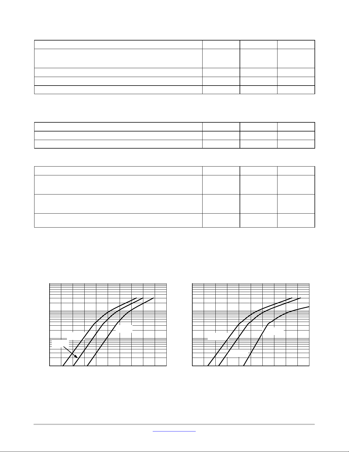
TYPICAL ELECTRICAL CHARACTERISTICS
100
10
25°C
1.0
, FORWARD CURRENT (A)
F
I
0.1
0.2 0.3 0.4 0.5 0.6 0.7 0.8 0.9 1.0 1.1 1.2
150°C
100°C
V
, INSTANTANEOUS VOLTAGE (V)
F
Figure 1. Typical Forward Voltage
100
10
25°C
1.0
, FORWARD CURRENT (A)
F
I
150°C
100°C
0.1
0.2 0.3 0.4 0.5 0.6 0.7 0.8 0.9 1 1.1 1.2
V
, INSTANTANEOUS VOLTAGE (V)
F
Figure 2. Maximum Forward Voltage
www.onsemi.com
2
Page 3

MBRS3201T3G, NRVBS3201T3G
TYPICAL ELECTRICAL CHARACTERISTICS (continued)
1E−1
1E−2
1E−3
1E−4
1E−5
1E−6
1E−7
, REVERSE CURRENT (A)
R
I
1E−8
1E−9
0 20 40 60 80 100 120 140 160 180 200
150°C
100°C
25°C
VR, REVERSE VOLTAGE (V)
Figure 3. Typical Reverse Current
1000
100
1.0E−01
1.0E−02
TC = 150°C
1.0E−03
TC = 25°C
1.0E−04
1.0E−05
, MAXIMUM REVERSE CURRENT (A)
R
I
1.0E−06
, REVERSE VOLTAGE (V)
V
R
Figure 4. Maximum Reverse Current
120 140 180 200
1600 20 40 60 80 100
10
C, CAPACITANCE (pF)
1.0
0 20 40 60 80 100 120 140 160 180 200
4.0
3.5
3.0
2.5
2.0
1.5
1.0
0.5
, AVERAGE POWER DISSIPATION (W)
0
FO
P
0 0.5 1 1.5 2 2.5 3 3.5 4 4.5 5
IO, AVERAGE FORWARD CURRENT
SQUARE
DC
Figure 6. Power Dissipation
VR, REVERSE VOLTAGE (V)
Figure 5. Typical Capacitance
7
6
5
4
SQUAREWAVE
3
2
1
, AVERAGE FORWARD CURRENT (A)
F
0
I
80 90 100 110 120 130 140 150 160
DC
TL, LEAD TEMPERATURE (°C)
Figure 7. Derating Curve
www.onsemi.com
3
Page 4

MECHANICAL CASE OUTLINE
PACKAGE DIMENSIONS
SCALE 1:1
SMC 2−LEAD
CASE 403AC
ISSUE B
DATE 27 JUL 2017
H
E
E
D
A1
DETAIL A
TOP VIEW
DETAIL A
A2
L
SIDE VIEW
b
END VIEW
RECOMMENDED
SOLDERING FOOTPRINT*
8.750
0.344
3.790
2X
0.149
2.250
2X
0.089
*For additional information on our Pb−Free strategy and soldering
details, please download the ON Semiconductor Soldering and
Mounting Techniques Reference Manual, SOLDERRM/D.
ǒ
inches
mm
Ǔ
SCALE 4:1
NOTES:
1. DIMENSIONING AND TOLERANCING PER ANME Y14.5M, 1994.
2. CONTROLLING DIMENSION: INCHES.
3. DIMENSIONS D AND E DO NOT INCLUDE MOLD FLASH. MOLD
FLASH SHALL NOT EXCEED 0.254mm PER SIDE.
4. DIMENSIONS D AND E TO BE DETERMINED AT DATUM H.
5. DIMENSION b SHALL BE MEASURED WITHIN THE AREA
DETERMINED BY DIMENSION L.
MILLIMETERS
DIMA2MIN MAX MIN
A 1.95 2.61 0.077 0.103
c
A
A1 0.05 0.20 0.002
1.90 2.41 0.075
b 2.90 3.20 0.114
c 0.15 0.41 0.006
D 5.55 6.25 0.219
E 6.60 7.15 0.260
H
7.75 8.15 0.305 0.321
E
L 0.75 1.60 0.030
INCHES
MAX
0.008
0.095
0.126
0.016
0.246
0.281
0.063
GENERIC
MARKING DIAGRAM*
AYWW
XXXXG
G
XXXX = Specific Device Code
A = Assembly Location
Y = Year
WW = Work Week
G = Pb−Free Package
(Note: Microdot may be in either location)
*This information is generic. Please refer to
device data sheet for actual part marking.
Pb−Free indicator, “G” or microdot “ G”,
may or may not be present.
DOCUMENT NUMBER:
DESCRIPTION:
ON Semiconductor and are trademarks of Semiconductor Components Industries, LLC dba ON Semiconductor or its subsidiaries in the United States and/or other countries.
ON Semiconductor reserves the right to make changes without further notice to any products herein. ON Semiconductor makes no warranty, representation or guarantee regarding
the suitability of its products for any particular purpose, nor does ON Semiconductor assume any liability arising out of the application or use of any product or circuit, and specifically
disclaims any and all liability, including without limitation special, consequential or incidental damages. ON Semiconductor does not convey any license under its patent rights nor the
rights of others.
© Semiconductor Components Industries, LLC, 2019
98AON97675F
SMC 2−LEAD
Electronic versions are uncontrolled except when accessed directly from the Document Repository.
Printed versions are uncontrolled except when stamped “CONTROLLED COPY” in red.
PAGE 1 OF 1
www.onsemi.com
Page 5

ON Semiconductor and are trademarks of Semiconductor Components Industries, LLC dba ON Semiconductor or its subsidiaries in the United States and/or other countries.
ON Semiconductor owns the rights to a number of patents, trademarks, copyrights, trade secrets, and other intellectual property. A listing of ON Semiconductor ’s product/patent
coverage may be accessed at www.onsemi.com/site/pdf/Patent−Marking.pdf
ON Semiconductor makes no warranty, representation or guarantee regarding the suitability of its products for any particular purpose, nor does ON Semiconductor assume any liability
arising out of the application or use of any product or circuit, and specifically disclaims any and all liability, including without limitation special, consequential or incidental damages.
Buyer is responsible for its products and applications using ON Semiconductor products, including compliance with all laws, regulations and safety requirements or standards,
regardless of any support or applications information provided by ON Semiconductor. “Typical” parameters which may be provided in ON Semiconductor data sheets and/or
specifications can and do vary in different applications and actual performance may vary over time. All operating parameters, including “Typicals” must be validated for each customer
application by customer’s technical experts. ON Semiconductor does not convey any license under its patent rights nor the rights of others. ON Semiconductor products are not
designed, intended, or authorized for use as a critical component in life support systems or any FDA Class 3 medical devices or medical devices with a same or similar classification
in a foreign jurisdiction or any devices intended for implantation in the human body. Should Buyer purchase or use ON Semiconductor products for any such unintended or unauthorized
application, Buyer shall indemnify and hold ON Semiconductor and its officers, employees, subsidiaries, affiliates, and distributors harmless against all claims, costs, damages, and
expenses, and reasonable attorney fees arising out of, directly or indirectly, any claim of personal injury or death associated with such unintended or unauthorized use, even if such
claim alleges that ON Semiconductor was negligent regarding the design or manufacture of the part. ON Semiconductor is an Equal Opportunity/Affirmative Action Employer. This
literature is subject to all applicable copyright laws and is not for resale in any manner.
. ON Semiconductor reserves the right to make changes without further notice to any products herein.
PUBLICATION ORDERING INFORMATION
LITERATURE FULFILLMENT:
Email Requests to: orderlit@onsemi.com
ON Semiconductor Website: www.onsemi.com
TECHNICAL SUPPORT
North American Technical Support:
Voice Mail: 1 800−282−9855 Toll Free USA/Canada
Phone: 011 421 33 790 2910
Europe, Middle East and Africa Technical Support:
Phone: 00421 33 790 2910
For additional information, please contact your local Sales Representative
◊
www.onsemi.com
1
 Loading...