

Page 1
MBRB20200CTG,
SBRB20200CTT4G
S
witch-mode
Power Rectifier
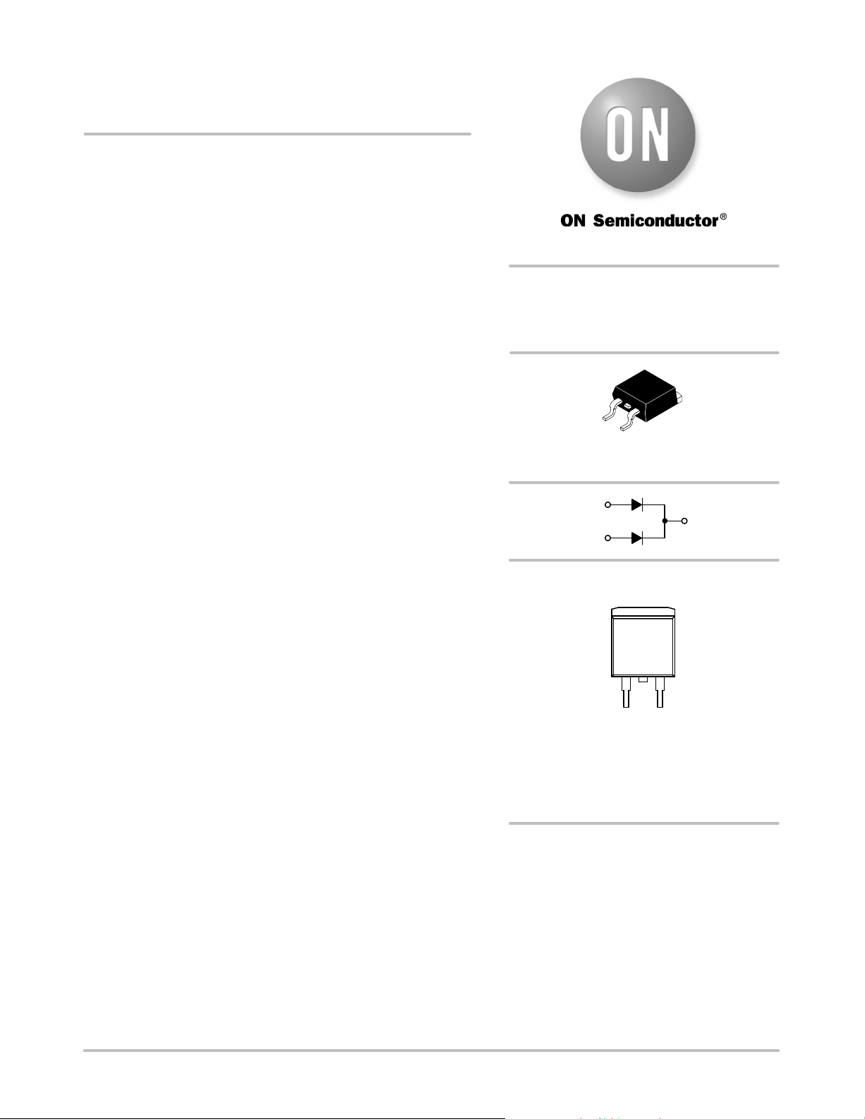
Dual Schottky Rectifier
This device uses the Schottky Barrier technology with a platinum
barrier metal. This state−of−the−art device is designed for use in high
frequency switching power supplies and converters with up to 48 V
outputs. They block up to 200 V and offer improved Schottky
performance at frequencies from 250 kHz to 5.0 MHz.
Features
200 V Blocking Voltage
Low Forward Voltage Drop
Guardring for Stress Protection and High dv/dt Capability
(10,000 V/ms)
Dual Diode Construction − Terminals 1 and 3 Must be Connected for
Parallel Operation at Full Rating
AEC−Q101 Qualified and PPAP Capable
SBRB Prefix for Automotive and Other Applications Requiring
Unique Site and Control Change Requirements
All Packages are Pb−Free*
http://onsemi.com
SCHOTTKY BARRIER
RECTIFIER
20 AMPERES, 200 V
D2PAK
CASE 418B
1
4
3
Mechanical Characteristics:
Case: Epoxy, Molded, Epoxy Meets UL 94 V−0
Weight: 1.7 Grams (Approximately)
Finish: All External Surfaces Corrosion Resistant and Terminal
Leads are Readily Solderable
Lead and Mounting Surface Temperature for Soldering
Purposes: 260C Max. for 10 Seconds
Device Meets MSL1 Requirements
ESD Rating:
Human Body Model = 3B
Machine Model = C
MARKING DIAGRAM
AY WW
B20200G
AKA
A = Assembly Location
Y = Year
WW = Work Week
B20200 = Device Code
G = Pb−Free Package
AKA = Diode Polarity
ORDERING INFORMATION
See detailed ordering and shipping information in the package
dimensions section on page 2 of this data sheet.
*For additional information on our Pb−Free strategy and soldering details, please
download the ON Semiconductor Soldering and Mounting Techniques
Reference Manual, SOLDERRM/D.
Semiconductor Components Industries, LLC, 2012
January, 2012 − Rev. 7
1 Publication Order Number:
MBRB20200CT/D
Page 2
MBRB20200CTG, SBRB20200CTT4G
MAXIMUM RATINGS (Per Leg)
Rating
Peak Repetitive Reverse Voltage
Working Peak Reverse Voltage
DC Blocking Voltage
Average Rectified Forward Current
(At Rated V
Per Leg
, TC = 134C)
R
Per Device
Peak Repetitive Forward Current
(At Rated V
Per Leg
, Square Wave, 20 kHz, TC = +137C)
R
Nonrepetitive Peak Surge Current
(Surge Applied at Rated Load Conditions Halfwave, Single Phase, 60 Hz)
Peak Repetitive Reverse Surge Current (2.0 ms, 1.0 kHz)
Storage Temperature Range T
Operating Junction Temperature T
Voltage Rate of Change (Rated VR) dv/dt 10,000
Stresses exceeding Maximum Ratings may damage the device. Maximum Ratings are stress ratings only. Functional operation above the
Recommended Operating Conditions is not implied. Extended exposure to stresses above the Recommended Operating Conditions may affect
device reliability.
THERMAL CHARACTERISTICS (Per Leg)
Characteristic
Thermal Resistance, Junction−to−Case
Symbol Value Unit
V
V
I
F(AV)
RRM
RWM
V
R
200 V
A
10
20
I
FRM
A
20
I
FSM
I
RRM
stg
150
1.0 A
−65 to +175 C
J
−65 to +150 C
A
V/ms
Symbol Value Unit
R
q
JC
2.0 C/W
ELECTRICAL CHARACTERISTICS (Per Leg)
Characteristic
Maximum Instantaneous Forward Voltage (Note 1)
(IF = 10 A, TC = 25C)
(IF = 10 A, TC = 125C)
(IF = 20 A, TC = 25C)
(IF = 20 A, TC = 125C)
Maximum Instantaneous Reverse Current (Note 1)
(Rated dc Voltage, T
(Rated dc Voltage, TC = 125C)
= 25C)
C
Symbol Value Unit
V
F
0.9
V
0.8
1.0
0.9
I
R
1.0
mA
50
DYNAMIC CHARACTERISTICS (Per Leg)
Capacitance
(V
= −5.0 V, TC = 25C, Frequency = 1.0 MHz)
R
1. Pulse Test: Pulse Width = 300 ms, Duty Cycle 2.0%.
C
T
pF
500
ORDERING INFORMATION
Device Package Shipping
MBRB20200CTG D2PAK
50 Units / Rail
(Pb−Free)
MBRB20200CTT4G D2PAK
800 Units / Tape & Reel
(Pb−Free)
SBRB20200CTT4G D2PAK
800 Units / Tape & Reel
(Pb−Free)
†For information on tape and reel specifications, including part orientation and tape sizes, please refer to our Tape and Reel Packaging
Specifications Brochure, BRD8011/D.
†
http://onsemi.com
2
Page 3

MBRB20200CTG, SBRB20200CTT4G
100
70
50
TJ = 150C
20
TJ = 125C
10
7
5
TJ = 100C
TJ = 25C
2
F
I , INSTANEOUS FORWARD CURRENT (AMP)
1
0.2 0.4 0.6 0.8 1
vF, INSTANTANEOUS VOLTAGE (V)
Figure 1. Typical Forward Voltage (Per Leg)
40
36
32
28
24
20
16
12
8
4
0
F(AV)
P , AVERAGE POWER DISSIPATION (WATTS)
0 5 10 15 20 25 30 35
TJ = 125C
I
PK
= 20
I
AV
I
, AVERAGE FORWARD CURRENT (A)
F(AV)
SQUARE
10
Figure 3. Forward Power Dissipation
WAVE
10,000
TJ = 150C
1,000
TJ = 125C
100
TJ = 100C
10
1
R
I , REVERSE CURRENT ( A)
0.1
TJ = 25C
0.01
20 40 60 80 100 120 140 160 180 200
0
VR, REVERSE CURRENT (V)
Figure 2. Typical Reverse Current (Per Leg)
25
20
dc
15
SQUARE
WAVE
10
5
F(AV)
I , AVERAGE FORWARD CURRENT (AMPS)
0
90 100 110 120 130 140 150 160
TC, CASE TEMPERATURE (C)
RATED VOLTAGE
R
q
dc
= 2C/W
JC
Figure 4. Current Derating, Case
20
R
16C/W
q
JA =
RATED VOLTAGE
16
8
dc
SQUARE
WAVE
12
4
F(AV)
0
I , AVERAGE FORWARD CURRENT (AMPS)
0 25 50 75 100 125 150 175
T
, AMBIENT TEMPERATURE (C)
A
Figure 5. Current Derating, Ambient
500
400
300
200
C, CAPACITANCE (pF)
100
0
1 2 5 10 20 50 70 100
http://onsemi.com
3
TJ = 25C
VR, REVERSE VOLTAGE (V)
Figure 6. Typical Capacitance (Per Leg)
Page 4

MECHANICAL CASE OUTLINE
PACKAGE DIMENSIONS
D2PAK 3
CASE 418B−04
ISSUE L
DATE 17 FEB 2015
SCALE 1:1
−T−
SEATING
PLANE
−B−
G
NOTES:
C
E
V
4
W
A
231
S
K
W
J
D
3 PL
0.13 (0.005) T
VARIABLE
CONFIGURATION
ZONE
M
M
M
B
H
R
L
N P
L
M
1. DIMENSIONING AND TOLERANCING
PER ANSI Y14.5M, 1982.
2. CONTROLLING DIMENSION: INCH.
3. 418B−01 THRU 418B−03 OBSOLETE,
NEW STANDARD 418B−04.
DIM MIN MAX MIN MAX
A 0.340 0.380 8.64 9.65
B 0.380 0.405 9.65 10.29
C 0.160 0.190 4.06 4.83
D 0.020 0.035 0.51 0.89
E 0.045 0.055 1.14 1.40
F 0.310 0.350 7.87 8.89
G 0.100 BSC 2.54 BSC
H 0.080 0.110 2.03 2.79
J 0.018 0.025 0.46 0.64
K 0.090 0.110 2.29 2.79
L 0.052 0.072 1.32 1.83
M 0.280 0.320 7.11 8.13
N 0.197 REF 5.00 REF
P 0.079 REF 2.00 REF
R 0.039 REF 0.99 REF
S 0.575 0.625 14.60 15.88
V 0.045 0.055 1.14 1.40
MILLIMETERSINCHES
U
L
M
STYLE 1:
PIN 1. BASE
2. COLLECTOR
3. EMITTER
4. COLLECTOR
F
VIEW W−W VIEW W−W VIEW W−W
123
STYLE 2:
PIN 1. GATE
2. DRAIN
3. SOURCE
4. DRAIN
STYLE 3:
PIN 1. ANODE
2. CATHODE
3. ANODE
4. CATHODE
F
STYLE 4:
PIN 1. GATE
2. COLLECTOR
3. EMITTER
4. COLLECTOR
STYLE 5:
PIN 1. CATHODE
2. ANODE
3. CATHODE
4. ANODE
F
STYLE 6:
PIN 1. NO CONNECT
2. CATHODE
3. ANODE
4. CATHODE
MARKING INFORMATION AND FOOTPRINT ON PAGE 2
DOCUMENT NUMBER:
DESCRIPTION:
ON Semiconductor and are trademarks of Semiconductor Components Industries, LLC dba ON Semiconductor or its subsidiaries in the United States and/or other countries.
ON Semiconductor reserves the right to make changes without further notice to any products herein. ON Semiconductor makes no warranty, representation or guarantee regarding
the suitability of its products for any particular purpose, nor does ON Semiconductor assume any liability arising out of the application or use of any product or circuit, and specifically
disclaims any and all liability, including without limitation special, consequential or incidental damages. ON Semiconductor does not convey any license under its patent rights nor the
rights of others.
98ASB42761B
D2PAK 3
Electronic versions are uncontrolled except when accessed directly from the Document Repository.
Printed versions are uncontrolled except when stamped “CONTROLLED COPY” in red.
PAGE 1 OF 2
© Semiconductor Components Industries, LLC, 2019
www.onsemi.com
Page 5

D2PAK 3
CASE 418B−04
ISSUE L
GENERIC
MARKING DIAGRAM*
DATE 17 FEB 2015
xx
xxxxxxxxx
AWLYWWG
xxxxxxxxG
AYWW
IC Standard
xx = Specific Device Code
A = Assembly Location
WL = Wafer Lot
Y = Year
WW = Work Week
G = Pb−Free Package
AKA = Polarity Indicator
*This information is generic. Please refer to
device data sheet for actual part marking.
Pb−Free indicator, “G” or microdot “ G”,
may or may not be present.
SOLDERING FOOTPRINT*
10.49
AYWW
xxxxxxxxG
AKA
Rectifier
8.38
16.155
2X
3.504
2X
1.016
5.080
PITCH
DIMENSIONS: MILLIMETERS
*For additional information on our Pb−Free strategy and soldering
details, please download the ON Semiconductor Soldering and
Mounting Techniques Reference Manual, SOLDERRM/D.
DOCUMENT NUMBER:
DESCRIPTION:
ON Semiconductor and are trademarks of Semiconductor Components Industries, LLC dba ON Semiconductor or its subsidiaries in the United States and/or other countries.
ON Semiconductor reserves the right to make changes without further notice to any products herein. ON Semiconductor makes no warranty, representation or guarantee regarding
the suitability of its products for any particular purpose, nor does ON Semiconductor assume any liability arising out of the application or use of any product or circuit, and specifically
disclaims any and all liability, including without limitation special, consequential or incidental damages. ON Semiconductor does not convey any license under its patent rights nor the
rights of others.
98ASB42761B
D2PAK 3
Electronic versions are uncontrolled except when accessed directly from the Document Repository.
Printed versions are uncontrolled except when stamped “CONTROLLED COPY” in red.
PAGE 2 OF 2
© Semiconductor Components Industries, LLC, 2019
www.onsemi.com
Page 6

ON Semiconductor and are trademarks of Semiconductor Components Industries, LLC dba ON Semiconductor or its subsidiaries in the United States and/or other countries.
ON Semiconductor owns the rights to a number of patents, trademarks, copyrights, trade secrets, and other intellectual property. A listing of ON Semiconductor’s product/patent
coverage may be accessed at www.onsemi.com/site/pdf/Patent−Marking.pdf
ON Semiconductor makes no warranty, representation or guarantee regarding the suitability of its products for any particular purpose, nor does ON Semiconductor assume any liability
arising out of the application or use of any product or circuit, and specifically disclaims any and all liability, including without limitation special, consequential or incidental damages.
Buyer is responsible for its products and applications using ON Semiconductor products, including compliance with all laws, regulations and safety requirements or standards,
regardless of any support or applications information provided by ON Semiconductor. “Typical” parameters which may be provided in ON Semiconductor data sheets and/or
specifications can and do vary in different applications and actual performance may vary over time. All operating parameters, including “Typicals” must be validated for each customer
application by customer’s technical experts. ON Semiconductor does not convey any license under its patent rights nor the rights of others. ON Semiconductor products are not
designed, intended, or authorized for use as a critical component in life support systems or any FDA Class 3 medical devices or medical devices with a same or similar classification
in a foreign jurisdiction or any devices intended for implantation in the human body. Should Buyer purchase or use ON Semiconductor products for any such unintended or unauthorized
application, Buyer shall indemnify and hold ON Semiconductor and its officers, employees, subsidiaries, affiliates, and distributors harmless against all claims, costs, damages, and
expenses, and reasonable attorney fees arising out of, directly or indirectly, any claim of personal injury or death associated with such unintended or unauthorized use, even if such
claim alleges that ON Semiconductor was negligent regarding the design or manufacture of the part. ON Semiconductor is an Equal Opportunity/Affirmative Action Employer. This
literature is subject to all applicable copyright laws and is not for resale in any manner.
. ON Semiconductor reserves the right to make changes without further notice to any products herein.
PUBLICATION ORDERING INFORMATION
LITERATURE FULFILLMENT:
Email Requests to: orderlit@onsemi.com
ON Semiconductor Website: www.onsemi.com
TECHNICAL SUPPORT
North American Technical Support:
Voice Mail: 1 800−282−9855 Toll Free USA/Canada
Phone: 011 421 33 790 2910
Europe, Middle East and Africa Technical Support:
Phone: 00421 33 790 2910
For additional information, please contact your local Sales Representative
◊
www.onsemi.com
1
 Loading...