

Page 1
MBD110DWT1G,
MBD330DWT1G,
MBD770DWT1G
Preferred Device
Dual Schottky Barrier
Diodes
Application circuit designs are moving toward the consolidation of
device count and into smaller packages. The new SOT−363 package is
a solution which simplifies circuit design, reduces device count, and
reduces board space by putting two discrete devices in one small
six−leaded package. The SOT−363 is ideal for low−power surface
mount applications where board space is at a premium, such as
portable products.
Surface Mount Comparisons:
SOT−363 SOT−23
Area (mm2) 4.6 7.6
Max Package PD (mW) 120 225
Device Count 2 1
Space Savings:
Package 1 SOT−23 2 SOT−23
SOT−363 40% 70%
http://onsemi.com
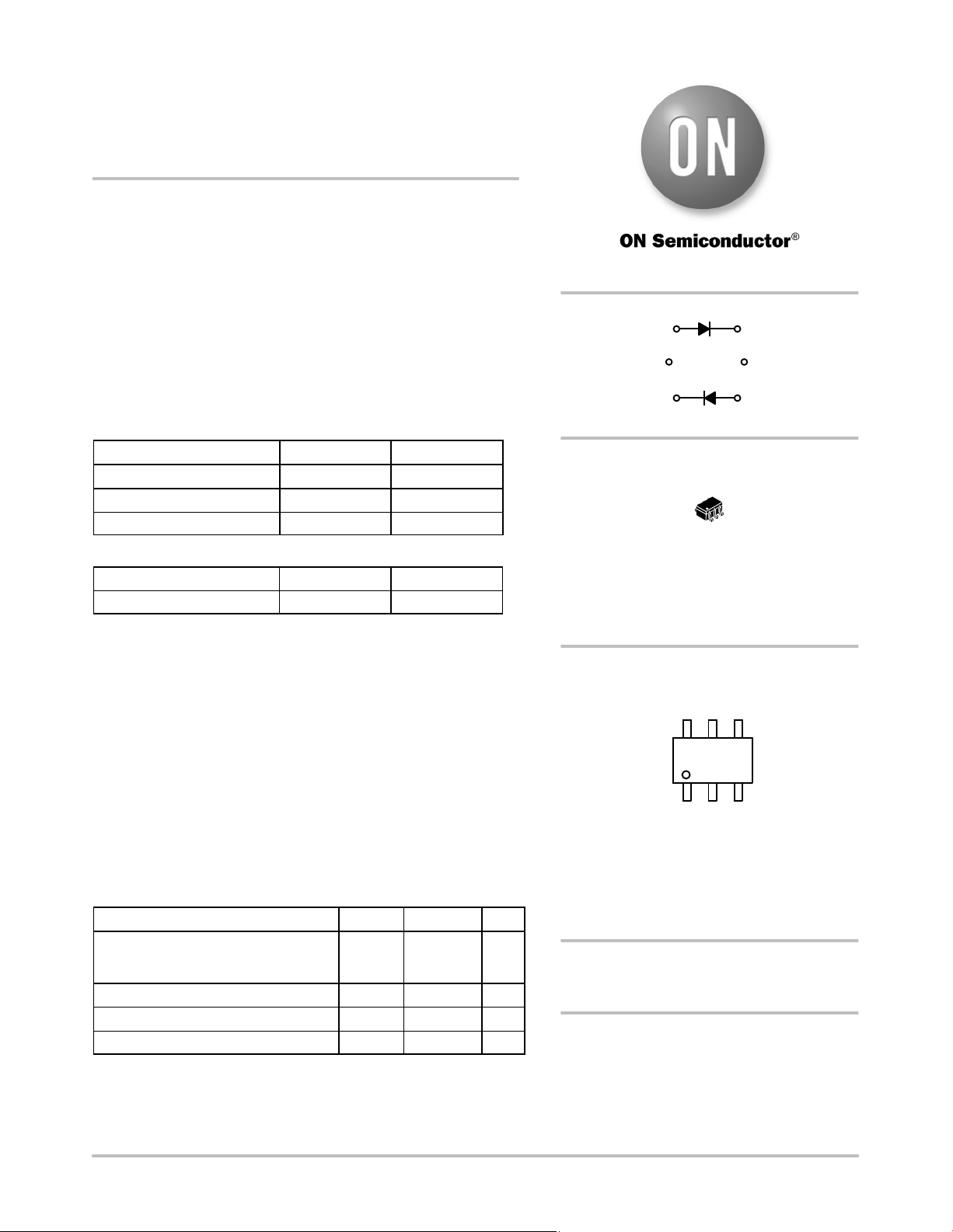
Anode 1 6 Cathode
N/C 2 5 N/C
Cathode 3 4 Anode
1
SC−88 / SOT−363
CASE 419B
STYLE 6
The MBD110DW, MBD330DW, and MBD770DW devices are
spin−offs of our popular MMBD101LT1, MMBD301LT1, and
MMBD701LT1 SOT−23 devices. They are designed for
high−efficiency UHF and VHF detector applications. Readily
available to many other fast switching RF and digital applications.
Features
• Extremely Low Minority Carrier Lifetime
• Very Low Capacitance
• Low Reverse Leakage
• These Devices are Pb−Free, Halogen Free/BFR Free and are RoHS
Compliant
MAXIMUM RATINGS
Rating Symbol Value Unit
Reverse Voltage MBD110DWT1G
MBD330DWT1G
MBD770DWT1G
Forward Power Dissipation TA = 25°C P
Junction Temperature T
Storage Temperature Range T
Stresses exceeding Maximum Ratings may damage the device. Maximum
Ratings are stress ratings only. Functional operation above the Recommended
Operating Conditions is not implied. Extended exposure to stresses above the
Recommended Operating Conditions may affect device reliability.
V
R
F
J
stg
7.0
30
70
120 mW
−55 to +125 °C
−55 to +150 °C
V
MARKING DIAGRAM
6
xx M G
G
1
xx = Device Code
Refer to Ordering Table,
page 2
M = Date Code
G = Pb−Free Package
(Note: Microdot may be in either location)
ORDERING INFORMATION
See detailed ordering and shipping information in the package
dimensions section on page 2 of this data sheet.
Preferred devices are recommended choices for future use
and best overall value.
© Semiconductor Components Industries, LLC, 2009
October, 2009 − Rev. 6
1 Publication Order Number:
MBD110DWT1/D
Page 2
MBD110DWT1G, MBD330DWT1G, MBD770DWT1G
ELECTRICAL CHARACTERISTICS (T
= 25°C unless otherwise noted)
A
Characteristic
Reverse Breakdown Voltage
= 10 mA) MBD110DWT1G
(I
R
MBD330DWT1G
MBD770DWT1G
Diode Capacitance
(V
= 0, f = 1.0 MHz, Note 1) MBD110DWT1G
R
Total Capacitance
(V
= 15 Volts, f = 1.0 MHz) MBD330DWT1G
R
(VR = 20 Volts, f = 1.0 MHz) MBD770DWT1G
Reverse Leakage
(V
= 3.0 V) MBD110DWT1G
R
(VR = 25 V) MBD330DWT1G
(VR = 35 V) MBD770DWT1G
Noise Figure
(f = 1.0 GHz, Note 2) MBD110DWT1G
Forward Voltage
(I
= 10 mA) MBD110DWT1G
F
(I
= 1.0 mA) MBD330DWT1G
F
(I
= 10 mA)
F
(I
= 1.0 mA) MBD770DWT1G
F
(I
= 10 mA)
F
Symbol Min Typ Max Unit
V
(BR)R
C
D
C
T
I
R
NF
7.0
30
70
10
−
−
− 0.88 1.0
−
−
−
−
−
0.9
0.5
0.02
13
9.0
−
−
−
1.5
1.0
0.25
200
200
V
pF
pF
mA
nA
nA
dB
− 6.0 −
V
F
−
−
−
−
−
0.5
0.38
0.52
0.42
0.7
0.6
0.45
0.6
0.5
1.0
V
ORDERING INFORMATION
Device Marking Package Shipping
MBD110DWT1G
M4
MBD330DWT1G
T4
MBD770DWT1G
H5
SC−88 / SOT−363
(Pb−Free)
SC−88 / SOT−363
(Pb−Free)
SC−88 / SOT−363
(Pb−Free)
3000 Units / Tape & Reel
†For information on tape and reel specifications, including part orientation and tape sizes, please refer to our Tape and Reel Packaging
Specifications Brochure, BRD8011/D.
†
http://onsemi.com
2
Page 3

MBD110DWT1G, MBD330DWT1G, MBD770DWT1G
TYPICAL CHARACTERISTICS
MBD110DWT1G
1.0
0.7
0.5
m
0.2
0.1
0.07
0.05
, REVERSE LEAKAGE ( A)I
R
0.02
0.01
VR = 3.0 V
MBD110DWT1G
TA, AMBIENT TEMPERATURE (°C)
Figure 1. Reverse Leakage
1.0
0.9
0.8
CAPACITANCE (pF)
,
D
C
0.7
MBD110DWT1G
0.6
0 1.0 2.0 3.0 4.0
VR, REVERSE VOLTAGE (VOLTS)
100
10
TA = 85°C
1.0
F
0.1
130110 12090
0.3 0.4 0.5 0.6
VF, FORWARD VOLTAGE (VOLTS)
TA = -40°C
TA = 25°C
MBD110DWT1G
0.7 0.830 40 50 60 70 80 100
Figure 2. Forward Voltage
11
10
9
8
7
6
5
4
NF, NOISE FIGURE (dB) , FORWARD CURRENT (mA)I
3
2
1
0.1 0.2 0.5 1.0 2.0 5.0 10
LOCAL OSCILLATOR FREQUENCY = 1.0 GHz
(Test Circuit Figure 5)
MBD110DWT1G
PLO, LOCAL OSCILLATOR POWER (mW)
Figure 3. Capacitance
UHF
NOISE SOURCE
H.P. 349A
NOISE
FIGURE METER
H.P. 342A
Figure 5. Noise Figure Test Circuit
LOCAL
OSCILLATOR
DIODE IN
TUNED
MOUNT
IF AMPLIFIER
NF = 1.5 dB
f = 30 MHz
http://onsemi.com
Figure 4. Noise Figure
NOTES ON TESTING AND SPECIFICATIONS
Note 1 − C
Note 2 − Noise figure measured with diode under test in tuned di-
Note 3 − LS is measured on a package having a short instead
3
and CT are measured using a capacitance
D
bridge (Boonton Electronics Model 75A or equivalent).
ode mount using UHF noise source and local oscillator
(LO) frequency of 1.0 GHz. The LO power is adjusted
for 1.0 mW. IF amplifier NF = 1.5 dB, f = 30 MHz, see
Figure 5.
of a die, using an impedance bridge (Boonton Radio
Model 250A RX Meter).
Page 4

MBD110DWT1G, MBD330DWT1G, MBD770DWT1G
TYPICAL CHARACTERISTICS
MBD330DWT1G
2.8
MBD330DWT1G
2.4
2.0
1.6
1.2
0.8
, TOTAL CAPACITANCE (pF)C
T
0.4
0
VR, REVERSE VOLTAGE (VOLTS)
f = 1.0 MHz
Figure 6. Total Capacitance
10
MBD330DWT1G
m
1.0
0.1
TA = 100°C
TA = 75°C
500
MBD330DWT1G
400
KRAKAUER METHOD
300
200
100
, MINORITY CARRIER LIFETIME (ps)t
0
3024 2718
0204060
10 30 50 70 90
IF, FORWARD CURRENT (mA)
80 1000 3.0 6.0 9.0 12 15 21
Figure 7. Minority Carrier Lifetime
100
MBD330DWT1G
TA = -40°C
10
TA = 85°C
, REVERSE LEAKAGE ( A)I
R
0.01
0.001
TA = 25°C
VR, REVERSE VOLTAGE (VOLTS)
Figure 8. Reverse Leakage
1.0
, FORWARD CURRENT (mA)I
F
30
0.1
0.2 0.4 0.6 0.8 1.0 1.20 6.0 12 18 24
TA = 25°C
VF, FORWARD VOLTAGE (VOLTS)
Figure 9. Forward Voltage
http://onsemi.com
4
Page 5

MBD110DWT1G, MBD330DWT1G, MBD770DWT1G
TYPICAL CHARACTERISTICS
MBD770DWT1G
2.0
MBD770DWT1G
1.6
1.2
0.8
, TOTAL CAPACITANCE (pF)C
T
0.4
0
VR, REVERSE VOLTAGE (VOLTS) IF, FORWARD CURRENT (mA)
f = 1.0 MHz
500
MBD770DWT1G
400
KRAKAUER METHOD
300
200
100
, MINORITY CARRIER LIFETIME (ps)t
0
0204060
10 30 50 70 90
80 1000 5.0 10 15 20 25 35 5040 4530
Figure 10. Total Capacitance Figure 11. Minority Carrier Lifetime
10
MBD770DWT1G
m
1.0
0.1
TA = 100°C
TA = 75°C
100
10
MBD770DWT1G
TA = 85°C
TA = -40°C
, REVERSE LEAKAGE ( A)I
0.01
R
0.001
TA = 25°C
0 10203040
, REVERSE VOLTAGE (VOLTS) VF, FORWARD VOLTAGE (VOLTS)
V
R
Figure 12. Reverse Leakage Figure 13. Forward Voltage
1.0
, FORWARD CURRENT (mA)I
F
0.1
50
0.2 0.4 0.8 1.2 1.6 2.0
TA = 25°C
http://onsemi.com
5
Page 6

MBD110DWT1G, MBD330DWT1G, MBD770DWT1G
PACKAGE DIMENSIONS
SC−88 / SC−70 / SOT−363
CASE 419B−02
ISSUE W
D
e
654
H
E
123
−E−
b
6 PL
MM
E0.2 (0.008)
A3
C
A
A1
L
NOTES:
1. DIMENSIONING AND TOLERANCING PER ANSI
Y14.5M, 1982.
2. CONTROLLING DIMENSION: INCH.
3. 419B−01 OBSOLETE, NEW STANDARD 419B−02.
MILLIMETERS
DIM MIN NOM MAX
A 0.80 0.95 1.10
A1 0.00 0.05 0.10
A3
b 0.10 0.21 0.30
C 0.10 0.14 0.25
D 1.80 2.00 2.20
E 1.15 1.25 1.35
e 0.65 BSC
L 0.10 0.20 0.30
H
STYLE 6:
0.20 REF 0.008 REF
2.00 2.10 2.20
E
PIN 1. ANODE 2
2. N/C
3. CATHODE 1
4. ANODE 1
5. N/C
6. CATHODE 2
INCHES
MIN NOM MAX
0.031 0.037 0.043
0.000 0.002 0.004
0.004 0.008 0.012
0.004 0.005 0.010
0.070 0.078 0.086
0.045 0.049 0.053
0.026 BSC
0.004 0.008 0.012
0.078 0.082 0.086
SOLDERING FOOTPRINT*
0.50
0.0197
0.65
0.025
0.65
0.025
0.40
0.0157
1.9
0.0748
SCALE 20:1
ǒ
inches
mm
Ǔ
*For additional information on our Pb−Free strategy and soldering
details, please download the ON Semiconductor Soldering and
Mounting Techniques Reference Manual, SOLDERRM/D.
ON Semiconductor and are registered trademarks of Semiconductor Components Industries, LLC (SCILLC). SCILLC reserves the right to make changes without further notice
to any products herein. SCILLC makes no warranty, representation or guarantee regarding the suitability of its products for any particular purpose, nor does SCILLC assume any liability
arising out of the application or use of any product or circuit, and specifically disclaims any and all liability, including without limitation special, consequential or incidental damages.
“Typical” parameters which may be provided in SCILLC data sheets and/or specifications can and do vary in different applications and actual performance may vary over time. All
operating parameters, including “Typicals” must be validated for each customer application by customer’s technical experts. SCILLC does not convey any license under its patent rights
nor the rights of others. SCILLC products are not designed, intended, or authorized for use as components in systems intended for surgical implant into the body, or other applications
intended to support or sustain life, or for any other application in which the failure of the SCILLC product could create a situation where personal injury or death may occur. Should
Buyer purchase or use SCILLC products for any such unintended or unauthorized application, Buyer shall indemnify and hold SCILLC and its officers, employees, subsidiaries, affiliates,
and distributors harmless against all claims, costs, damages, and expenses, and reasonable attorney fees arising out of, directly or indirectly, any claim of personal injury or death
associated with such unintended or unauthorized use, even if such claim alleges that SCILLC was negligent regarding the design or manufacture of the part. SCILLC is an Equal
Opportunity/Affirmative Action Employer. This literature is subject to all applicable copyright laws and is not for resale in any manner.
PUBLICATION ORDERING INFORMATION
LITERATURE FULFILLMENT:
Literature Distribution Center for ON Semiconductor
P.O. Box 5163, Denver, Colorado 80217 USA
Phone: 303−675−2175 or 800−344−3860 Toll Free USA/Canada
Fax: 303−675−2176 or 800−344−3867 Toll Free USA/Canada
Email: orderlit@onsemi.com
N. American Technical Support: 800−282−9855 Toll Free
USA/Canada
Europe, Middle East and Africa Technical Support:
Phone: 421 33 790 2910
Japan Customer Focus Center
Phone: 81−3−5773−3850
http://onsemi.com
ON Semiconductor Website: www.onsemi.com
Order Literature: http://www.onsemi.com/orderlit
For additional information, please contact your local
Sales Representative
MBD110DWT1/D
6
 Loading...