

Page 1
MAX809 Series,
MAX810 Series
Very Low Supply Current
3−Pin Microprocessor
Reset Monitors
The MAX809 and MAX810 are cost−effective system supervisor
circuits designed to monitor VCC in digital systems and provide a reset
signal to the host processor when necessary. No external components
are required.
The reset output is driven active within 10 msec of VCC falling
through the reset voltage threshold. Reset is maintained active for a
timeout period which is trimmed by the factory after VCC rises above
the reset threshold. The MAX810 has an active−high RESET output
while the MAX809 has an active−low RESET output. Both devices
are available in SOT−23 and SC−70 packages.
The MAX809/810 are optimized to reject fast transient glitches on
the VCC line. Low supply current of 0.5 mA (V
devices suitable for battery powered applications.
Features
• Precision V
Monitor for 1.5 V, 1.8 V, 2.5 V, 3.0 V, 3.3 V, and 5.0 V
CC
Supplies
• Precision Monitoring Voltages from 1.2 V to 4.9 V Available
in 100 mV Steps
• Four Guaranteed Minimum Power−On Reset Pulse Width Available
(1 ms, 20 ms, 100 ms, and 140 ms)
• RESET Output Guaranteed to V
= 1.0 V.
CC
• Low Supply Current
• Compatible with Hot Plug Applications
• V
Transient Immunity
CC
• No External Components
• Wide Operating Temperature: −40°C to 105°C
• Pb−Free Packages are Available
Typical Applications
• Computers
• Embedded Systems
• Battery Powered Equipment
• Critical Microprocessor Power Supply Monitoring
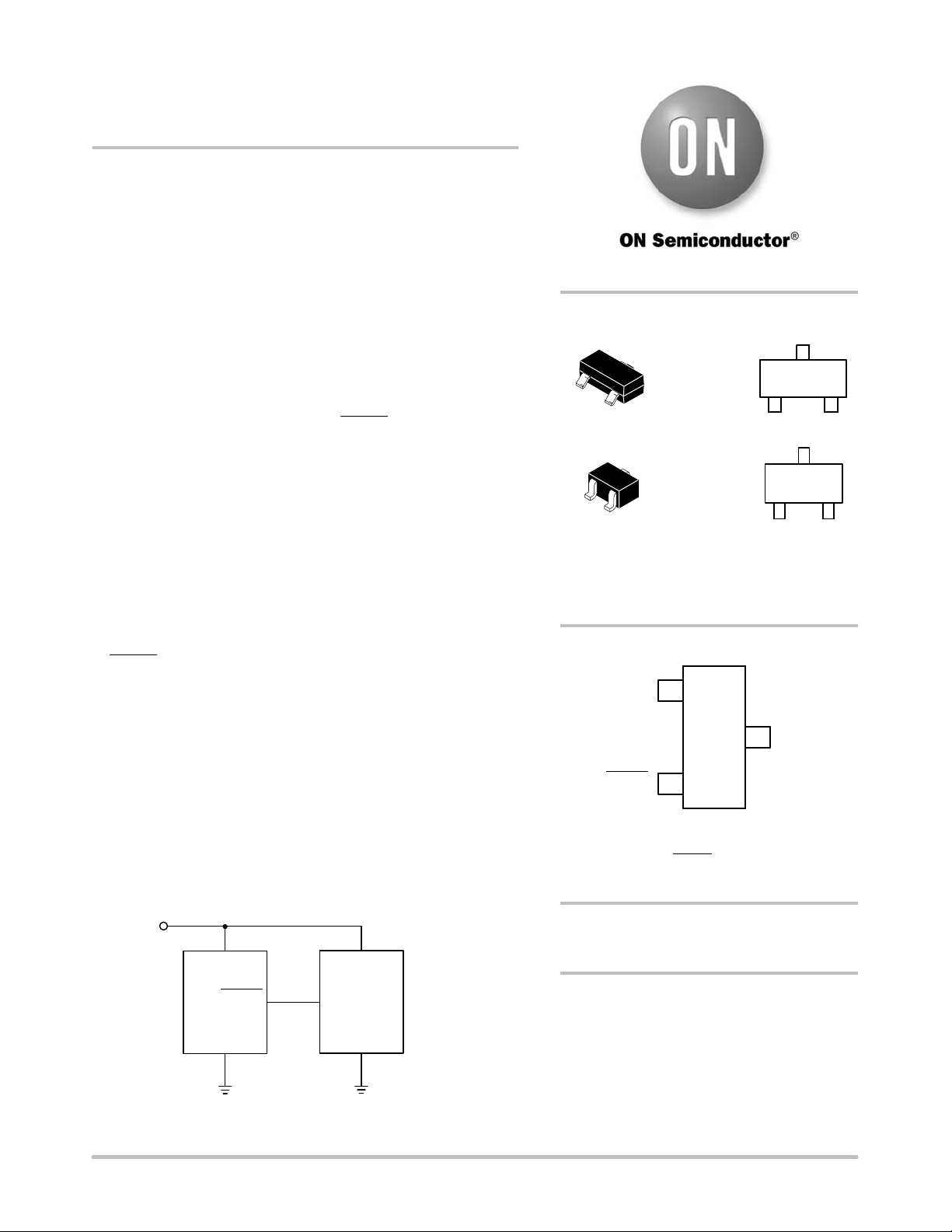
V
CC
V
CC
MAX809/810
RESET
RESET
PROCESSOR
RESET
INPUT
= 3.2 V) makes these
CC
V
CC
http://onsemi.com
MARKING
DIAGRAM
3
SOT−23
(TO−236)
1
2
xxx = Specific Device Code
M = Date Code
G = Pb−Free Package
(Note: Microdot may be in either location)
GND
RESET
RESET
NOTE: RESET is for MAX809
ORDERING INFORMATION
See detailed ordering and shipping information in the package
dimensions section on page 8 of this data sheet.
DEVICE MARKING INFORMATION
See general marking information in the device marking
section on page 8 of this data sheet.
CASE 318
SC−70
(SOT−323)
CASE 419
PIN CONFIGURATION
1
2
SOT−23/SC−70
(Top View)
RESET is for MAX810
3
xxx MG
G
21
xx MG
G
1
V
3
CC
GND GND
Figure 1. Typical Application Diagram
© Semiconductor Components Industries, LLC, 2007
February, 2007 − Rev. 15
1 Publication Order Number:
MAX809S/D
Page 2
MAX809 Series, MAX810 Series
T
T
R
qJA
PIN DESCRIPTION
Pin No. Symbol Description
1 GND Ground
2 RESET (MAX809) RESET output remains low while VCC is below the reset voltage threshold, and for a reset timeout
2 RESET (MAX810) RESET output remains high while VCC is below the reset voltage threshold, and for a reset timeout
3 V
CC
ABSOLUTE MAXIMUM RATINGS
Power Supply Voltage (VCC to GND) V
RESET Output Voltage (CMOS) −0.3 to (VCC + 0.3) V
Input Current, V
Output Current, RESET 20 mA
dV/dt (VCC) 100
Thermal Resistance, Junction−to−Air (Note 1) SOT−23
Operating Junction Temperature Range T
Storage Temperature Range T
Lead Temperature (Soldering, 10 Seconds) T
ESD Protection
Latchup Current Maximum Rating: Following Specification JESD78 Class II
Stresses exceeding Maximum Ratings may damage the device. Maximum Ratings are stress ratings only. Functional operation above the
Recommended Operating Conditions is not implied. Extended exposure to stresses above the Recommended Operating Conditions may affect
device reliability.
1. This based on a 35x35x1.6mm FR4 PCB with 10mm2 of 1 oz copper traces under natural convention conditions and a single component
characterization.
2. The maximum package power dissipation limit must not be exceeded.
CC
Human Body Model (HBM): Following Specification JESD22−A114
Machine Model (MM): Following Specification JESD22−A115
*
J(max)
P
+
D
period after VCC rises above reset threshold
period after VCC rises above reset threshold
Supply Voltage (Typ)
Rating Symbol Value Unit
CC
−0.3 to 6.0 V
20 mA
SC−70
R
q
JA
J
stg
sol
301
314
−40 to +105 °C
−65 to +150 °C
+260 °C
2000
200
I
Positive
Latchup
Negative
A
with T
J(max)
= 150°C
200
200
V/msec
°C/W
V
mA
http://onsemi.com
2
Page 3
MAX809 Series, MAX810 Series
ELECTRICAL CHARACTERISTICS T
Characteristic Symbol Min Typ Max Unit
VCC Range
TA = 0°C to +70°C
TA = −40°C to +105°C
Supply Current
VCC = 3.3 V
TA = −40°C to +85°C
TA = 85°C to +105°C
VCC = 5.5 V
TA = −40°C to +85°C
TA = 85°C to +105°C
Reset Threshold (Vin Decreasing) (Note 4)
MAX809SN490
TA = +25°C
TA = −40°C to +85°C
TA = +85°C to +105°C
MAX8xxLTR, MAX8xxSQ463
TA = +25°C
TA = −40°C to +85°C
TA = +85°C to +105°C
MAX809HTR
TA = +25°C
TA = −40°C to +85°C
TA = +85°C to +105°C
MAX8xxMTR, MAX8xxSQ438
TA = +25°C
TA = −40°C to +85°C
TA = +85°C to +105°C
MAX809JTR, MAX8xxSQ400
TA = +25°C
TA = −40°C to +85°C
TA = +85°C to +105°C
MAX8xxTTR, MAX809SQ308
TA = +25°C
TA = −40°C to +85°C
TA = +85°C to +105°C
MAX8xxSTR, MAX8xxSQ293
TA = +25°C
TA = −40°C to +85°C
TA = +85°C to +105°C
MAX8xxRTR, MAX8xxSQ263
TA = +25°C
TA = −40°C to +85°C
TA = +85°C to +105°C
MAX809SN232, MAX809SQ232
TA = +25°C
TA = −40°C to +85°C
TA = +85°C to +105°C
MAX809SN160
TA = +25°C
TA = −40°C to +85°C
TA = +85°C to +105°C
MAX809SN120, MAX8xxSQ120
TA = +25°C
TA = −40°C to +85°C
TA = +85°C to +105°C
3. Production testing done at TA = 25°C, over temperature limits guaranteed by design.
4. Contact your ON Semiconductor sales representative for other threshold voltage options.
= −40°C to +105°C unless otherwise noted. Typical values are at TA = +25°C. (Note 3)
A
I
CC
V
TH
1.0
1.2
−
−
−
−
4.83
4.78
4.66
4.56
4.50
4.40
4.48
4.43
4.32
4.31
4.27
4.16
3.94
3.90
3.80
3.04
3.00
2.92
2.89
2.85
2.78
2.59
2.56
2.49
2.28
2.25
2.21
1.58
1.56
1.52
1.18
1.17
1.14
−
−
0.5
−
0.8
−
4.9
−
−
4.63
−
−
4.55 4.62
4.38 4.45
4.00
−
−
3.08
−
−
2.93
−
−
2.63
−
−
2.32
−
−
1.60
−
−
1.20
−
−
5.5
5.5
1.2
2.0
1.8
2.5
4.97
5.02
5.14
4.70
4.75
4.86
4.67
4.78
4.49
4.60
4.06
4.10
4.20
3.11
3.16
3.24
2.96
3.00
3.08
2.66
2.70
2.77
2.35
2.38
2.45
1.62
1.64
1.68
1.22
1.23
1.26
V
mA
V
http://onsemi.com
3
Page 4
MAX809 Series, MAX810 Series
ELECTRICAL CHARACTERISTICS (continued) T
= −40°C to +105°C unless otherwise noted. Typical values are at
A
TA = +25°C. (Note 5)
Characteristic Symbol Min Typ Max Unit
Detector Voltage Threshold Temperature Coefficient − 30 − ppm/°C
VCC to Reset Delay VCC = VTH to (VTH − 100 mV) − 10 −
Reset Active TimeOut Period (Note 6)
MAX8xxSN(Q)293D1
MAX8xxSN(Q)293D2
MAX8xxSN(Q)293D3
MAX8xxSN(Q)293
RESET Output Voltage Low (No Load) (MAX809)
VCC = VTH − 0.2 V
1.6 V v VTH v 2.0 V, I
2.1 V v VTH v 4.0 V, I
4.1 V v VTH v 4.9 V, I
SINK
SINK
SINK
= 0.5 mA
= 1.2 mA
= 3.2 mA
RESET Output Voltage High (No Load) (MAX809)
VCC = VTH + 0.2 V
1.6 V v VTH v 2.4 V, I
2.5 V v VTH v 4.9 V, I
SOURCE
SOURCE
= 200 mA
= 500 mA
RESET Output Voltage High (No Load) (MAX810)
VCC = VTH + 0.2 V
1.6 V v VTH v 2.4 V, I
2.5 V v VTH v 4.9 V, I
SOURCE
SOURCE
= 200 mA
= 500 mA
RESET Output Voltage Low (No Load) (MAX810)
VCC = VTH − 0.2 V
1.6 V v VTH v 2.0 V, I
2.1 V v VTH v 4.0 V, I
4.1 V v VTH v 4.9 V, I
SINK
SINK
SINK
= 0.5 mA
= 1.2 mA
= 3.2 mA
t
RP
V
OL
V
OH
V
OH
V
OL
1.0
20
100
140
−
3.3
−
−
−
330
460
− − 0.3 V
0.8 V
0.8 V
CC
CC
− − V
− − V
− − 0.3 V
66
msec
msec
5. Production testing done at TA = 25°C, over temperature limits guaranteed by design.
6. Contact your ON Semiconductor sales representative for timeout options availability for other threshold voltage options.
http://onsemi.com
4
Page 5

MAX809 Series, MAX810 Series
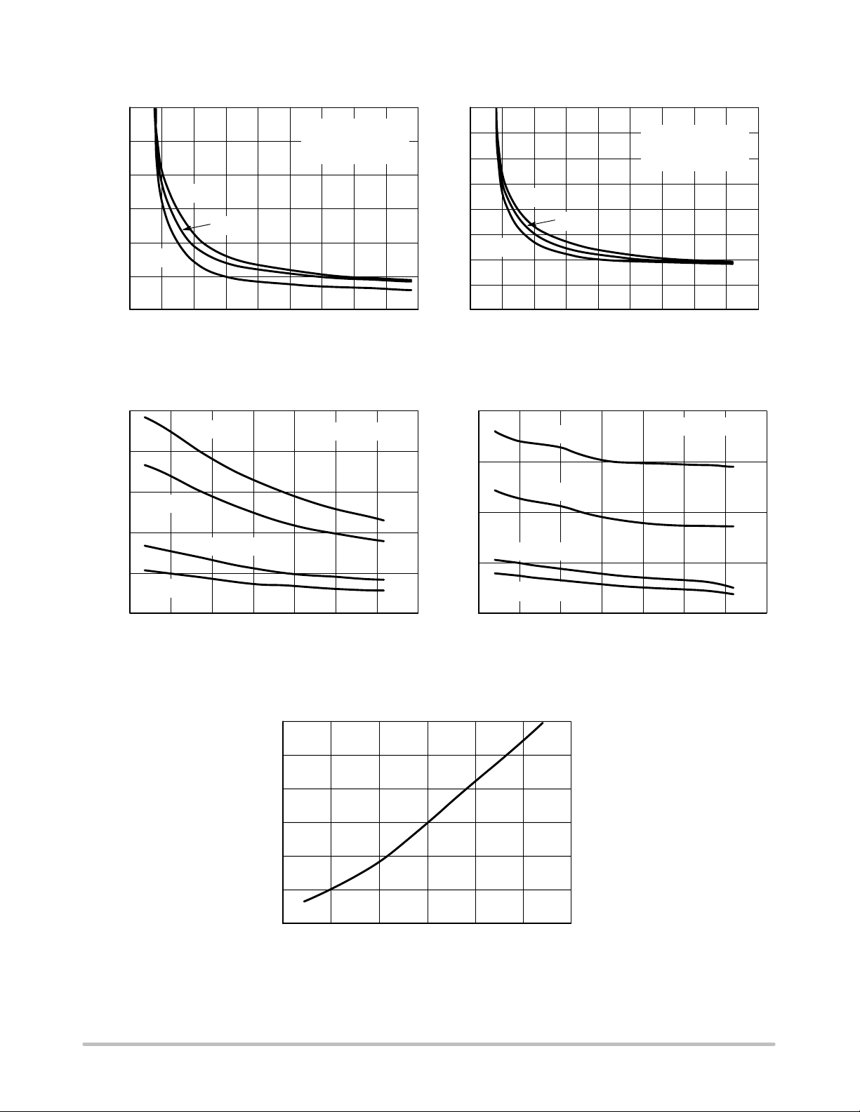
TYPICAL OPERATING CHARACTERISTICS
0.6
VTH = 1.2 V
0.5
0.4
0.3
0.2
SUPPLY CURRENT (mA)
0.1
0
0.5 1.5 2.5 3.5 4.5 6.5
SUPPLY VOLTAGE (V)
85°C
25°C
−40°C
Figure 2. Supply Current vs. Supply Voltage
0.35
VTH = 2.93 V
0.30
0.25
0.20
0.15
0.10
SUPPLY CURRENT (mA)
0.05
0
0.5 1.5 2.5 3.5 4.5 6.5
SUPPLY VOLTAGE (V)
85°C
25°C
−40°C
Figure 4. Supply Current vs. Supply Voltage Figure 5. Normalized Reset Threshold Voltage
0.35
0.30
0.25
0.20
0.15
0.10
SUPPLY CURRENT (mA)
0.05
5.5 5.5
VTH = 4.9 V
85°C
25°C
−40°C
0
0.5 1.5 2.5 3.5 4.5 6.5
SUPPLY VOLTAGE (V)
Figure 3. Supply Current vs. Supply Voltage
1.002
1.001
1.000
5.5
0.999
0.998
0.997
0.996
0.995
0.994
NORMALIZED THRESHOLD VOLTAGE
−50 −25 0 25 50 75
TEMPERATURE (°C)
VTH = 4.9 V
VTH = 1.2 V
vs. Temperature
100
0.40
MAX809L/M, VCC = 5.0 V
0.32
0.24
0.16
SUPPLY CURRENT (mA)
0.08
0
−50 −25 0 25 50
MAX809L/M/R/S/T, VCC = 1.0 V
TEMPERATURE (°C)
Figure 6. Supply Current vs. Temperature
(No Load, MAX809)
MAX809R/S/T, VCC = 3.3 V
75 100
http://onsemi.com
0.40
0.32
0.24
0.16
SUPPLY CURRENT (mA)
0.08
0
−50 −25 0 25 50
MAX810L/M, VCC = 5.0 V
MAX810R/S/T, VCC = 3.3 V
MAX810L/M/R/S/T, VCC = 1.0 V
TEMPERATURE (°C)
75
100
Figure 7. Supply Current vs. Temperature (No
Load, MAX810)
5
Page 6
MAX809 Series, MAX810 Series
TYPICAL OPERATING CHARACTERISTICS
30
VTH = 4.90 V
I
25
(mV)
CC
20
85°C
15
25°C
10
−40°C
5.0
OUTPUT VOLTAGE V
0
1.0 2.0 3.0
0.5 1.5 2.5 3.5 4.5 5.0
SUPPLY VOLTAGE (V)
= 500 mA
SINK
RESET ASSERTED
4.0 5.0
Figure 8. Output Voltage Low vs. Supply
Voltage
125
VOD = 10 mV
100
75
VOD = 20 mV
50
25
VOD = 200 mV
POWER−DOWN RESET DELAY (msec)
0
−50 −25 0 25 75 125
VOD = 100 mV
TEMPERATURE (°C)
VOD = VCC−V
Figure 10. Power−Down Reset Delay vs.
Temperature and Overdrive (V
= 1.2 V)
TH
100
TH
80
70
(mV)
OH
60
−V
CC
50
40
30
20
10
OUTPUT VOLTAGE V
0
0.5 1.5 2.5 3.5 4.5
85°C
25°C
−40°C
1.0 2.0 3.0 4.0
SUPPLY VOLTAGE (V)
VTH = 4.63 V
I
SOURCE
RESET ASSERTED
Figure 9. Output Voltage High vs. Supply
Voltage
400
VOD = 10 mV
300
VOD = 20 mV
200
VOD = 100 mV
100
VOD = 200 mV
POWER−DOWN RESET DELAY (msec)
0
−50 −25 0 25 50 75
TEMPERATURE (°C)
Figure 11. Power−Down Reset Delay vs.
Temperature and Overdrive (VTH = 4.9 V)
= 100 mA
VOD = VCC−V
10050
TH
125
1.3
1.2
1.1
1.0
0.9
0.8
0.7
−50 −25 0 25 50
NORMALIZED POWER−UP RESET TIMEOUT
TEMPERATURE (°C)
Figure 12. Normalized Power−Up Reset vs.
Temperature
http://onsemi.com
6
75 100
Page 7

MAX809 Series, MAX810 Series
V
MAXIMUM TRANSIENT DURATION (
sec)
0
APPLICATIONS INFORMA TION
VCC Transient Rejection
The MAX809 provides accurate VCC monitoring and
reset timing during power−up, power−down, and
brownout/sag conditions, and rejects negative−going
transients (glitches) on the power supply line. Figure 13
shows the maximum transient duration vs. maximum
negative excursion (overdrive) for glitch rejection. Any
combination of duration and overdrive which lies under the
curve will not generate a reset signal. Combinations above
the curve are detected as a brownout or power−down.
Typically, transient that goes 100 mV below the reset
threshold and lasts 5.0 ms or less will not cause a reset pulse.
Transient immunity can be improved by adding a capacitor
in close proximity to the VCC pin of the MAX809.
CC
V
TH
Overdrive
Duration
300
m
250
200
150
100
50
0
VTH = 4.9 V
VTH = 2.93 V
VTH = 1.2 V
10
11060
160 210 260 310 360
RESET COMPARATOR OVERDRIVE (mV)
Figure 13. Maximum Transient Duration vs.
Overdrive for Glitch Rejection at 25°C
RESET Signal Integrity During Power−Down
The MAX809 RESET output is valid to VCC = 1.0 V.
Below this voltage the output becomes an “open circuit” and
does not sink current. This means CMOS logic inputs to the
Microprocessor will be floating at an undetermined voltage.
Most digital systems are completely shutdown well above
this voltage. However, in situations where RESET must be
41
maintained valid to VCC = 0 V, a pull−down resistor must be
connected from RESET to ground to discharge stray
capacitances and hold the output low (Figure 14). This
resistor value, though not critical, should be chosen such that
it does not appreciably load RESET under normal operation
(100 kW will be suitable for most applications).
V
CC
V
CC
MAX809/810
RESET
RESET
GND
R1
100 k
Figure 14. Ensuring RESET Valid to VCC = 0 V
Processors With Bidirectional I/O Pins
Some Microprocessor’s have bidirectional reset pins.
Depending on the current drive capability of the processor
pin, an indeterminate logic level may result if t he r e i s a l o g i c
conflict. This can be avoided by adding a 4.7 kW resistor in
series with the output of the MAX809 (Figure 15). If there
are other components in the system which require a reset
signal, they should be buffered so as not to load the reset line.
If the other components are required to follow the reset I/O
of the Microprocessor, the buffer should be connected as
shown with the solid line.
BUFFER
V
CC
V
CC
MAX809/810
4.7 k
RESET
RESET
GND GND
Microprocessor
RESET
Figure 15. Interfacing to Bidirectional Reset I/O
BUFFERED RESET
TO OTHER SYSTEM
COMPONENTS
V
CC
http://onsemi.com
7
Page 8

MAX809 Series, MAX810 Series
ORDERING, MARKING AND THRESHOLD INFORMATION
Part Number VTH*
(V)
MAX809SN160T1 1.60 140−460
MAX809SN160T1G 1.60 140−460 SAA SOT23−3
MAX809SN232T1 2.32 140−460 SQP SOT23−3
MAX809SN232T1G 2.32 140−460 SQP SOT23−3
MAX809RTR 2.63 140−460 SPS SOT23−3
MAX809RTRG 2.63 140−460 SPS SOT23−3
MAX809STR 2.93 140−460 SPT SOT23−3
MAX809STRG 2.93 140−460 SPT SOT23−3
MAX809TTR 3.08 140−460 SPU SOT23−3
MAX809TTRG 3.08 140−460 SPU SOT23−3
MAX809JTR 4.00 140−460 SPR SOT23−3
MAX809JTRG 4.00 140−460 SPR SOT23−3
MAX809MTR 4.38 140−460 SPV SOT23−3
MAX809MTRG 4.38 140−460 SPV SOT23−3
MAX809HTR 4.55 140−460 SBD SOT23−3
MAX809HTRG 4.55 140−460 SBD SOT23−3
MAX809LTR 4.63 140−460 SPW SOT23−3
MAX809LTRG 4.63 140−460 SPW SOT23−3
MAX809SN490T1 4.90 140−460 SBH SOT23−3
MAX809SN490T1G 4.90 140−460 SBH SOT23−3
MAX809SN120T1G 1.20 140−460 SSO SOT23−3
MAX809SN293D1T1G 2.93 1−3.3 SSP SOT23−3
MAX809SN293D2T1G 2.93 20−66 SSQ SOT23−3
MAX809SN293D3T1G 2.93 100−330 SSR SOT23−3
MAX809SQ120T1G 1.20 140−460 ZD SC70−3
MAX809SQ232T1G 2.32 140−460 ZE SC70−3
MAX809SQ263T1G 2.63 140−460 ZF SC70−3
MAX809SQ293T1G 2.93 140−460 ZG SC70−3
MAX809SQ308T1G 3.08 140−460 ZH SC70−3
MAX809SQ400T1G 4.00 140−460 SZ SC70−3
MAX809SQ438T1G 4.38 140−460 ZI SC70−3
MAX809SQ463T1G 4.63 140−460 ZJ SC70−3
MAX809SQ293D1T1G 2.93 1−3.3 ZK SC70−3
MAX809SQ293D2T1G 2.93 20−66 ZL SC70−3
MAX809SQ293D3T1G 2.93 100−330 ZM SC70−3
†For information on tape and reel specifications,including part orientation and tape sizes, please refer to our Tape and Reel Packaging
Specifications Brochure, BRD8011/D.
*Contact your ON Semiconductor sales representative for other threshold voltage options.
Timeout*
(ms)
Description Marking Package Shipping
SAA SOT23−3
(Pb−Free)
(Pb−Free)
(Pb−Free)
(Pb−Free)
(Pb−Free)
(Pb−Free)
(Pb−Free)
(Pb−Free)
(Pb−Free)
Push−Pull RESET
(Pb−Free)
(Pb−Free)
(Pb−Free)
(Pb−Free)
(Pb−Free)
(Pb−Free)
(Pb−Free)
(Pb−Free)
(Pb−Free)
(Pb−Free)
(Pb−Free)
(Pb−Free)
(Pb−Free)
(Pb−Free)
(Pb−Free)
(Pb−Free)
3000 / Tape & Reel
†
http://onsemi.com
8
Page 9
MAX809 Series, MAX810 Series
ORDERING, MARKING AND THRESHOLD INFORMATION
Part Number VTH*
(V)
MAX810RTR 2.63 140−460
MAX810RTRG 2.63 140−460 SPX SOT23−3
MAX810STR 2.93 140−460 SPY SOT23−3
MAX810STRG 2.93 140−460 SPY SOT23−3
MAX810TTR 3.08 140−460 SPZ SOT23−3
MAX810TTRG 3.08 140−460 SPZ SOT23−3
MAX810MTR 4.38 140−460 SQA SOT23−3
MAX810MTRG 4.38 140−460 SQA SOT23−3
MAX810LTR 4.63 140−460 SQB SOT23−3
MAX810LTRG 4.63 140−460 SQB SOT23−3
MAX810SN120T1G 1.20 140−460 SSS SOT23−3
MAX810SN293D1T1G 2.93 1−3.3 SST SOT23−3
MAX810SN293D2T1G 2.93 20−66 SSU SOT23−3
MAX810SN293D3T1G 2.93 100−330 SSZ SOT23−3
MAX810SQ120T1G 1.20 140−460 ZN SC70−3
MAX810SQ263T1G 2.63 140−460 ZO SC70−3
MAX810SQ293T1G 2.93 140−460 ZP SC70−3
MAX810SQ438T1G 4.38 140−460 ZQ SC70−3
MAX810SQ463T1G 4.63 140−460 ZR SC70−3
MAX810SQ293D1T1G 2.93 1−3.3 ZS SC70−3
MAX810SQ293D2T1G 2.93 20−66 ZT SC70−3
MAX810SQ293D3T1G 2.93 100−330 ZU SC70−3
†For information on tape and reel specifications,including part orientation and tape sizes, please refer to our Tape and Reel Packaging
Specifications Brochure, BRD8011/D.
*Contact your ON Semiconductor sales representative for other threshold voltage options.
Timeout*
(ms)
Description Marking Package Shipping
SPX SOT23−3
(Pb−Free)
(Pb−Free)
(Pb−Free)
(Pb−Free)
(Pb−Free)
(Pb−Free)
Push−Pull RESET
(Pb−Free)
3000 / Tape & Reel
(Pb−Free)
(Pb−Free)
(Pb−Free)
(Pb−Free)
(Pb−Free)
(Pb−Free)
(Pb−Free)
(Pb−Free)
(Pb−Free)
(Pb−Free)
†
http://onsemi.com
9
Page 10

MAX809 Series, MAX810 Series
SOT−23 (TO236)
PACKAGE DIMENSIONS
CASE 318−08
ISSUE AN
D
H
SEE VIEW C
E
c
0.25
3
E
12
b
e
q
A
L
A1
L1
NOTES:
1. DIMENSIONING AND TOLERANCING PER ANSI
Y14.5M, 1982.
2. CONTROLLING DIMENSION: INCH.
3. MAXIMUM LEAD THICKNESS INCLUDES LEAD
FINISH THICKNESS. MINIMUM LEAD
THICKNESS IS THE MINIMUM THICKNESS OF
BASE MATERIAL.
4. 318−01 THRU −07 AND −09 OBSOLETE, NEW
STANDARD 318−08.
DIMAMIN NOM MAX MIN
A1 0.01 0.06 0.10 0.001
b 0.37 0.44 0.50 0.015
c 0.09 0.13 0.18 0.003
D 2.80 2.90 3.04 0.110
E 1.20 1.30 1.40 0.047
e 1.78 1.90 2.04 0.070
L 0.10 0.20 0.30 0.004
L1
H
E
MILLIMETERS
0.89 1.00 1.11 0.035
0.35 0.54 0.69 0.014 0.021 0.029
2.10 2.40 2.64 0.083 0.094 0.104
INCHES
NOM MAX
0.040 0.044
0.002 0.004
0.018 0.020
0.005 0.007
0.114 0.120
0.051 0.055
0.075 0.081
0.008 0.012
VIEW C
SOLDERING FOOTPRINT*
0.95
0.95
0.037
0.037
2.0
0.079
0.9
0.035
0.8
0.031
mm
ǒ
SCALE 10:1
inches
Ǔ
*For additional information on our Pb−Free strategy and soldering
details, please download the ON Semiconductor Soldering and
Mounting Techniques Reference Manual, SOLDERRM/D.
http://onsemi.com
10
Page 11

MAX809 Series, MAX810 Series
SC−70 (SOT−323)
PACKAGE DIMENSIONS
CASE 419−04
ISSUE M
0.05 (0.002)
D
e1
3
H
E
12
e
A1
E
b
A
A2
SOLDERING FOOTPRINT*
0.65
0.025
NOTES:
1. DIMENSIONING AND TOLERANCING PER ANSI
Y14.5M, 1982.
2. CONTROLLING DIMENSION: INCH.
DIMAMIN NOM MAX MIN
A1 0.00 0.05 0.10 0.000
A2 0.7 REF
b 0.30 0.35 0.40 0.012
c 0.10 0.18 0.25 0.004
D 1.80 2.10 2.20 0.071
E 1.15 1.24 1.35 0.045
e 1.20 1.30 1.40 0.047
e1
L
c
H
E
MILLIMETERS
0.80 0.90 1.00 0.032
0.65 BSC
0.425 REF
2.00 2.10 2.40 0.079 0.083 0.095
INCHES
NOM MAX
0.035 0.040
0.002 0.004
0.028 REF
0.014 0.016
0.007 0.010
0.083 0.087
0.049 0.053
0.051 0.055
0.026 BSC
0.017 REF
L
0.65
0.025
1.9
0.075
0.9
0.035
0.7
0.028
SCALE 10:1
ǒ
inches
mm
Ǔ
*For additional information on our Pb−Free strategy and soldering
details, please download the ON Semiconductor Soldering and
Mounting Techniques Reference Manual, SOLDERRM/D.
ON Semiconductor and are registered trademarks of Semiconductor Components Industries, LLC (SCILLC). SCILLC reserves the right to make changes without further notice
to any products herein. SCILLC makes no warranty, representation or guarantee regarding the suitability of its products for any particular purpose, nor does SCILLC assume any liability
arising out of the application or use of any product or circuit, and specifically disclaims any and all liability, including without limitation special, consequential or incidental damages.
“Typical” parameters which may be provided in SCILLC data sheets and/or specifications can and do vary in different applications and actual performance may vary over time. All
operating parameters, including “Typicals” must be validated for each customer application by customer’s technical experts. SCILLC does not convey any license under its patent rights
nor the rights of others. SCILLC products are not designed, intended, or authorized for use as components in systems intended for surgical implant into the body, or other applications
intended to support or sustain life, or for any other application in which the failure of the SCILLC product could create a situation where personal injury or death may occur. Should
Buyer purchase or use SCILLC products for any such unintended or unauthorized application, Buyer shall indemnify and hold SCILLC and its officers, employees, subsidiaries, affiliates,
and distributors harmless against all claims, costs, damages, and expenses, and reasonable attorney fees arising out of, directly or indirectly, any claim of personal injury or death
associated with such unintended or unauthorized use, even if such claim alleges that SCILLC was negligent regarding the design or manufacture of the part. SCILLC is an Equal
Opportunity/Affirmative Action Employer. This literature is subject to all applicable copyright laws and is not for resale in any manner.
PUBLICATION ORDERING INFORMATION
LITERATURE FULFILLMENT:
Literature Distribution Center for ON Semiconductor
P.O. Box 5163, Denver, Colorado 80217 USA
Phone: 303−675−2175 or 800−344−3860 Toll Free USA/Canada
Fax: 303−675−2176 or 800−344−3867 Toll Free USA/Canada
Email: orderlit@onsemi.com
N. American Technical Support: 800−282−9855 Toll Free
USA/Canada
Europe, Middle East and Africa Technical Support:
Phone: 421 33 790 2910
Japan Customer Focus Center
Phone: 81−3−5773−3850
ON Semiconductor Website: www.onsemi.com
Order Literature: http://www.onsemi.com/orderlit
For additional information, please contact your local
Sales Representative
http://onsemi.com
11
MAX809S/D
 Loading...