

Page 1
MAX707, MAX708
mP Supervisory Circuits
The MAX707/708 are cost−effective system supervisor circuits
designed to monitor V
to the host processor when necessary. No external components are
required.
The reset output is driven active within 20 msec of VCC falling
through the reset voltage threshold. Reset is maintained with 200 mS
of delay time after VCC rise above the reset threshold. The
MAX707/708 have a low quiescent current of 12 mA at VCC = 3.3 V,
an active−high RESET and active−low RESET with a push−pull
output. The output is guaranteed valid down to VCC = 1.0 V. The
MAX707/708 have a Manual Reset MR input and a +1.25 V threshold
detector for power−fail input PFI. These devices are available in a
Micro8 and SOIC−8 package.
Features
• Precision Supply−Voltage Monitor
MAX707: 4.63 V Reset Threshold Voltage
MAX708: Standard Reset Threshold Voltages (Typical):
4.38 V, 3.08 V, 2.93 V, 2.63 V
• Reset Threshold Available from 1.6 V to 4.9 V with 100 mV
Increments (Factory Option)
• 200 mS (Typ) Reset Timeout Delay
• 12 mA (V
= 3.3 V) Quiescent Current
CC
• Active_High and Active_Low Reset Output
• Guaranteed RESET_L and RESET Output Valid to V
• Voltage Monitor for Power−Fail or Low−Battery Warning
• 8 Pin SOIC or Micro8 Package
• Pb−Free Packages are Available
in digital systems and provide a reset signal
CC
= 1.0 V
CC
http://onsemi.com
8
1
xxx = Specific Device Code
A = Assembly Location
Y = Year
W = Week
G = Pb−Free Package
8
1
xxxxx = Specific Device Code
AL = Assembly Lot Code
Y = Year
W = Week
G = Pb−Free Package
(Note: Microdot may be in either location)
Micro8t
CUA SUFFIX
CASE 846A
SOIC−8
ESA SUFFIX
CASE 751
PIN CONFIGURATION
MARKING
DIAGRAMS
8
xxx
AYW
G
1
8
xxxxx
ALYWG
G
1
Applications
• Computers
• Embedded System
• Battery Powered Equipment
• Critical mP Power Supply Monitor
© Semiconductor Components Industries, LLC, 2005
August, 2005 − Rev. 4
Micro8
RESET
RESET
MR
V
CC
1
2
3
4
(Top View)
NC
8
PFO
7
PFI
6
GND
5
SOIC−8
MR
V
CC
GND
PFI
1
2
3
4
(Top View)
8
7
6
5
RESET
RESET
NC
PFO
ORDERING INFORMATION
See detailed ordering and shipping information in the package
dimensions section on page 8 of this data sheet.
1 Publication Order Number:
MAX707/D
Page 2
MR
T
T
R
qJA
MAX707, MAX708
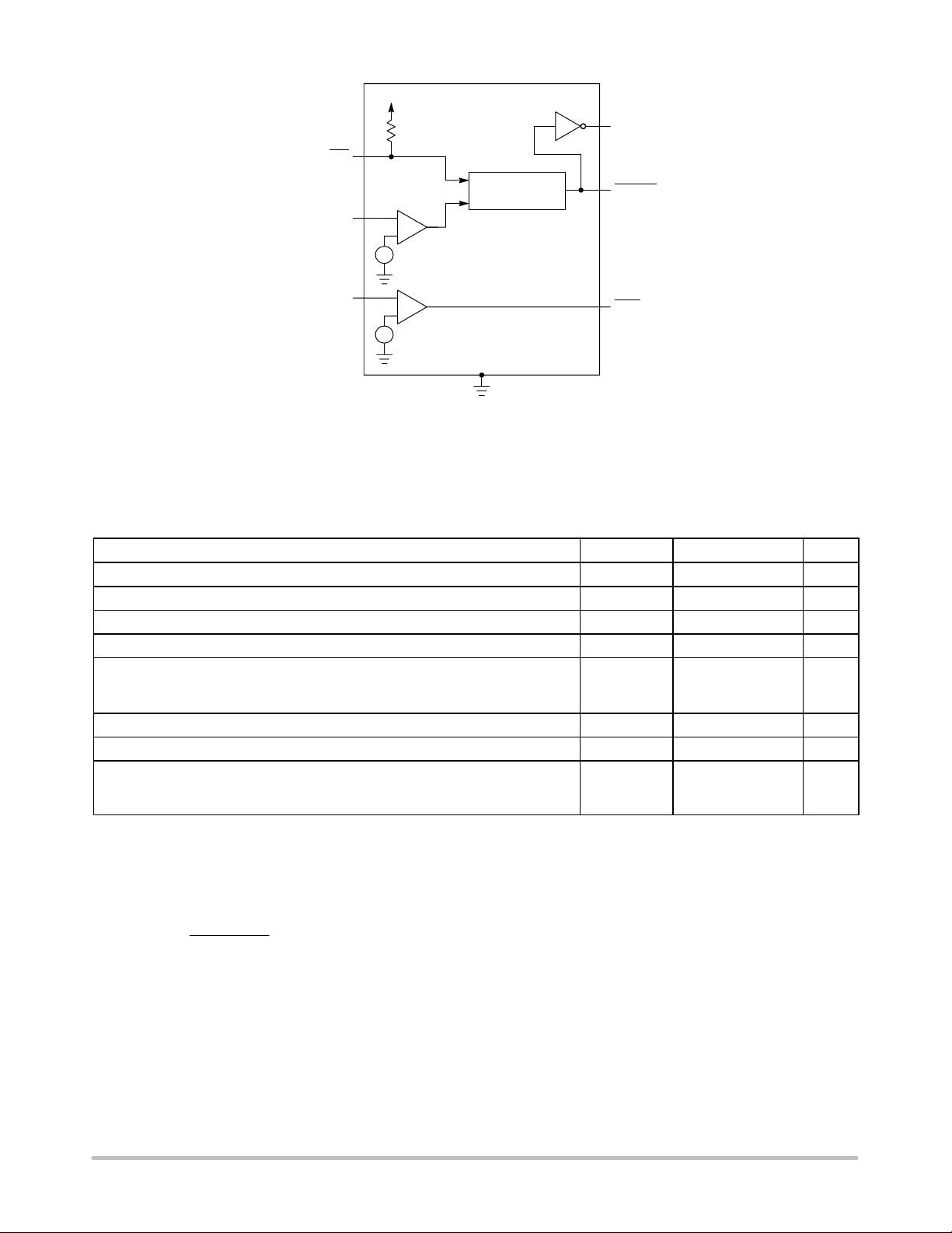
V
CC
RESET
RESET
GENERATOR
V
CC
+
RESET
−
V
TH
PFI
+
−
PFO
1.25 V
GND
Figure 1. Representative Block Diagram
MAXIMUM RATINGS (Note 1)
Rating Symbol Value Unit
Supply Voltage V
Output Voltage V
Output Current (All Outputs) I
Input Current (VCC and GND) I
Thermal Resistance Junction−to−Air
CC
out
out
in
R
q
JA
Micro8
SOIC−8
Operating Ambient Temperature T
Storage Temperature Range T
LatchUp Performance
A
stg
I
LATCHUP
Positive
Negative
Maximum ratings are those values beyond which device damage can occur. Maximum ratings applied to the device are individual stress limit
values (not normal operating conditions) and are not valid simultaneously. If these limits are exceeded, device functional operation is not implied,
damage may occur and reliability may be affected.
1. This device series contains ESD protection and exceeds the following tests:
Human Body Model 2000 V per MIL−STD−883, Method 3015.
Machine Model Method 200 V.
2. The maximum package power dissipation limit must not be exceeded.
*
J(max)
P
+
D
A
with T
J(max)
= 150°C
6.0 V
−0.3 to (VCC + 0.3) V
20 mA
20 mA
°C/W
248
187
−40 to +85 °C
−40 to +125 °C
mA
300
280
http://onsemi.com
2
Page 3
MAX707, MAX708
ELECTRICAL CHARACTERISTICS (V
= 1.0 V to 5.5 V, TA = −40°C to +85°C, unless otherwise noted. Typical values
CC
are at TA = 25°C, VCC = 3.3 V.)
Characteristics Symbol Min Typ Max Unit
Operating Voltage Range V
Supply Current
VCC = 3.3 V
VCC = 5.5 V
Reset Threshold
CC
I
CC
V
TH
1.0 − 5.5 V
−
−
12
16
22
28
MAX707
TA = +25°C
TA = −40°C to +85°C
4.56
4.50
4.63
4.70
4.75
MAX708
TA = +25°C
TA = −40°C to +85°C
4.31
4.25
4.38
4.45
4.50
MAX708T
TA = +25°C
TA = −40°C to +85°C
3.03
3.00
3.08
3.13
3.15
MAX708S
TA = +25°C
TA = −40°C to +85°C
2.89
2.85
2.93
2.97
3.00
MAX708R
TA = +25°C
TA = −40°C to +85°C
Reset Threshold Hysteresis V
VCC Falling Reset Delay (VCC = VTH + 0.2 V to VTH − 0.2 V) t
Reset Active Timeout Period t
RESET_L, RESET_H Output Low Voltage
VCC w 1.0 V, Iol = 100 mA
VCC u 2.7 V, Iol = 1.2 mA
VCC u 4.5 V, Iol = 3.2 mA
RESET_L, RESET_H Output High Voltage
VCC w 1.0 V, Ioh = 50 mA
VCC u 2.7 V, Ioh = 500 mA
VCC u 4.5 V, Ioh = 800 mA
MR_L Pull−up Resistance R
MR_L Pulse Width (VTH (max) t VCC t 5.5 V) t
HYS
PD
RP
V
V
MRI
MR
ol
oh
2.59
2.55
− 0.01 V
2.63
TH
2.67
2.70
− mV
− 20 −
140 200 330 mS
0.8 V
0.8 V
0.8 V
−
−
−
CC
CC
CC
−
−
−
−
−
−
0.3
0.3
0.3
−
−
−
50 − −
1.0 − −
MR_L Glitch Rejection (VTH (max) t VCC t 5.5 V) − − 0.1 −
MR_L High_level Input Threshold (VTH (max) t VCC t 5.5 V) V
MR_L Low_level Input Threshold (VTH (max) t VCC t 5.5 V) V
MR_L to RESET_L and RESET_H Output Delay
IH
IL
t
MD
0.7 V
CC
− − V
− − 0.3 V
− 0.2 −
CC
(VTH (max) t VCC t 5.5 V)
PFI Input Threshold (VCC = 3.3 V, PFI Falling) − 1.20 1.25 1.3 V
PFI Input Current − −250 0.01 250 nA
PFI to PFO Delay (VCC = 3.3 V, V
PFO_L Output Low Voltage
VCC = 2.7 V, Iol = 1.2 mA
VCC = 4.5 V, Iol = 3.2 mA
PFO_L Output High Voltage
VCC = 2.7 V, Ioh = 500 mA
VCC = 4.5 V, Ioh = 800 mA
OVERDRIVE
= 15 mV) − − 3.0 −
V
ol
V
oh
0.8 V
0.8 V
−
−
CC
CC
−
−
0.3
0.3
−
−
−
−
mA
V
mS
V
V
KW
mS
mS
V
mS
mS
V
V
http://onsemi.com
3
Page 4
MAX707, MAX708
Á
Á
Á
Á
Á
Á
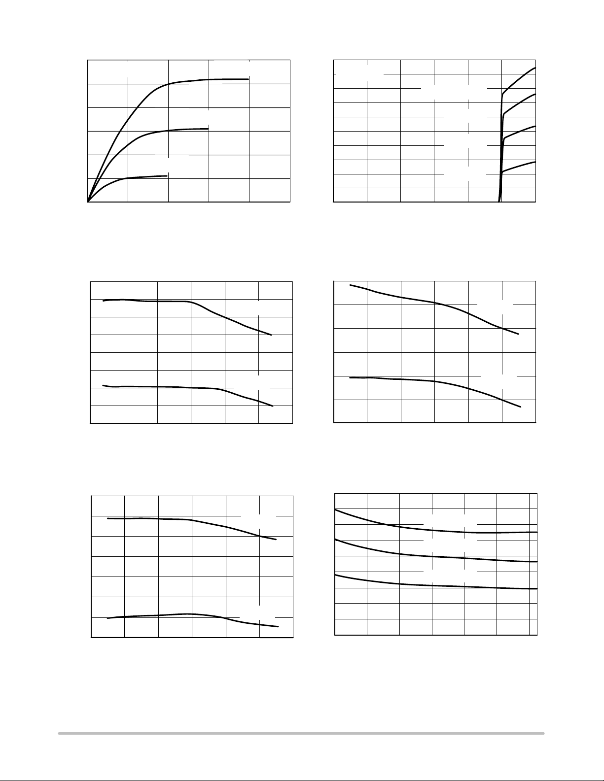
I
, OUTPUT SINK CURRENT (mA)
0
)
0
I
, OUTPUT SINK CURRENT (mA)
PIN DESCRIPTION (Pin No. with parentheses is for Micro8 package.)
Pin No. Symbol Description
1 (3)
ÁÁ
2 (4)
3 (5)
4 (6)
5 (7)
6 (8)
7 (1)
ÁÁ
8 (2)
MR
Á
V
CC
GND
PFI
PFO
NC
RESET
Á
RESET
Manual Reset Input. MR can be driven from TTL/CMOS logic or from a manual Reset switch. This input, when
floating, is internally pulled up to VCC with 50 kW resistor.
ББББББББББББББББББББББББББ
Supply Voltage: C = 100 nF is recommended as a bypass capacitor between VCC and GND.
Ground Reference
Power Fail Voltage Monitor Input. When PFI is less than 1.25 V, PFO goes low. Connect PFI to GND or VCC when
not used.
Power Fail Monitor Output. When PFI is less than 1.25 V, it goes low and sinks current. Otherwise, it remains high.
Non−connective Pin
Active Low RESET can be triggered by VCC below the threshold level or by a low signal on MR. It remains low for
ББББББББББББББББББББББББББ
200 ms (typ.) after VCC rises above the reset threshold.
Active high RESET output the inverse of RESET one.
3.0
TA = 25°C
2.5
2.0
1.5
1.0
0.5
OUT
0
0
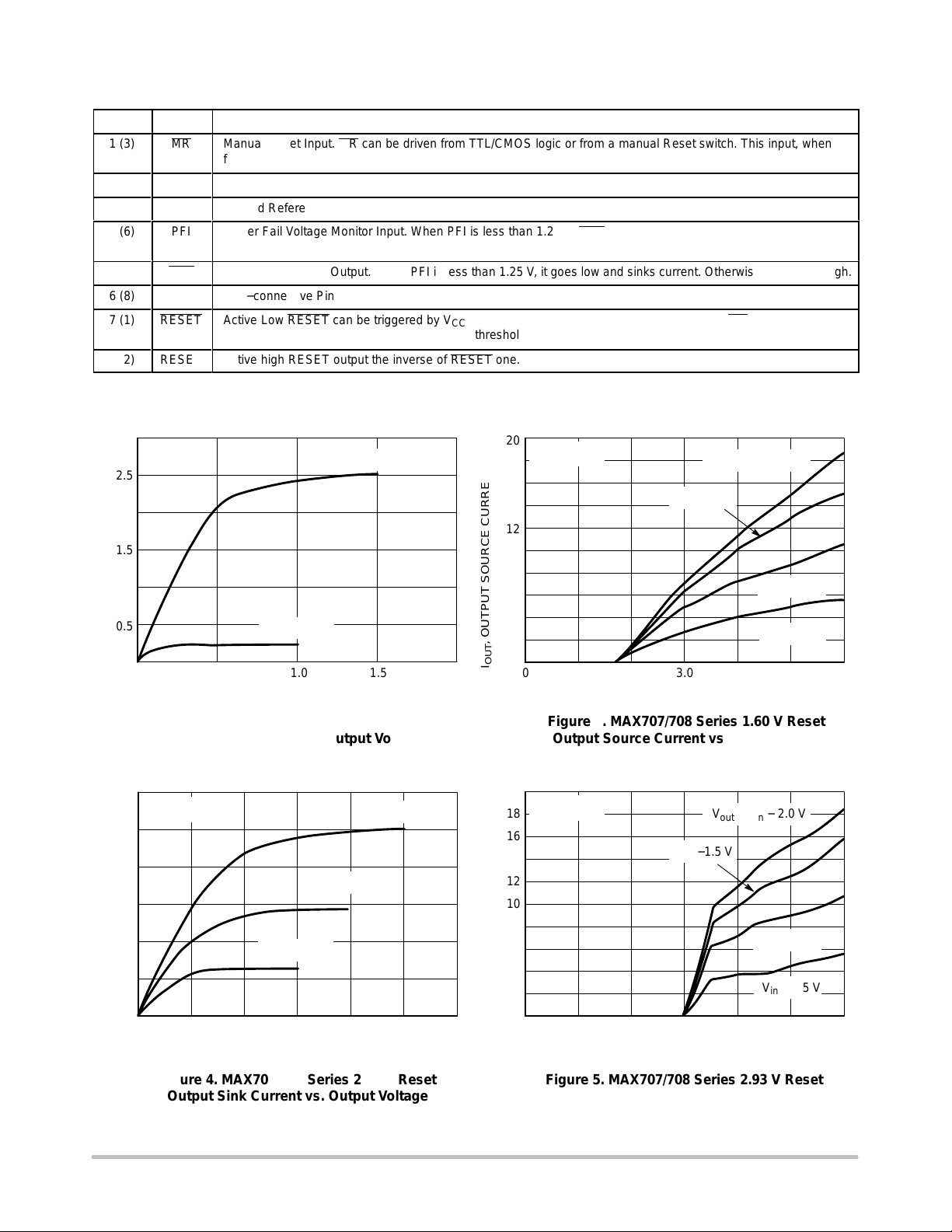
Figure 2. MAX707/708 Series 1.60 V Reset
12
10
OUT
Output Sink Current vs. Output Voltage
TA = 25°C
8
6
4
2
0
0.50
Vin = 1.0 V
0.5
V
, OUTPUT VOLTAGE (V)
out
1.0 1.5
Vin = 1.5 V
V
, OUTPUT VOLTAGE (V)
out
Vin = 1.5 V
Vin = 2.5 V
Vin = 2.0 V
2.01.0 1.5 2.5 3.0
20
TA = 25°C
18
16
14
12
10
8
6
4
, OUTPUT SOURCE CURRENT (mA
2
OUT
0
I
2.0
0
1.0 4.0
Figure 3. MAX707/708 Series 1.60 V Reset
Output Source Current vs. Input Voltage
20
TA = 25°C
18
16
14
12
10
8
6
4
2
, OUTPUT SOURCE CURRENT (mA)
out
I
0
0.0 1.0 6.
V
= Vin − 2.0 V
out
Vin − 1.5 V
2.0
3.0
Vin, INPUT VOLTAGE (V)
V
= Vin − 2.0 V
out
Vin −1.5 V
Vin − 1.0 V
Vin − 0.5 V
2.0 3.0 4.0 5.0
Vin, INPUT VOLTAGE (V)
Vin − 1.0 V
Vin − 0.5 V
5.0 6.
Figure 4. MAX707/708 Series 2.93 V Reset
Output Sink Current vs. Output Voltage
http://onsemi.com
4
Figure 5. MAX707/708 Series 2.93 V Reset
Output Source Current vs. Input Voltage
Page 5
MAX707, MAX708
I
, OUTPUT SINK CURRENT (mA)
)
0
0
30
TA = 25°C
25
20
15
10
5
out
0
0.0 4.03.02.01.0 5.0 0.0 1.0 6.
Figure 6. MAX707/708 Series 4.90 V Reset
Output Sink Current vs. Output Voltage
1625
1620
1615
1610
Vin = 3.0 V
Vin = 2.0 V
V
, OUTPUT VOLTAGE (V)
out
Vin = 4.0 V
V
DET+
20
18
TA = 25°C
16
14
V
out
12
10
8
6
4
2
, OUTPUT SOURCE CURRENT (mA
out
I
0
2.0 3.0 4.0 5.0
Vin, INPUT VOLTAGE (V)
Figure 7. MAX707/708 Series 4.90 V Reset
Output Source Current vs. Input Voltage
3120
3110
3100
= Vin − 2.0 V
Vin − 1.5 V
Vin − 1.0 V
Vin − 0.5 V
V
DET+
1605
1600
V
1595
DET−
1590
1585
, DETECTOR THRESHOLD VOLTAGE (VOLTS)
DET
V
−50
0−25
TA, AMBIENT TEMPERATURE (°C)
25
50 75
Figure 8. MAX707/708 Series 1.60 V Detector
Threshold Voltage vs. Temperature
5020
5000
V
DET+
4980
4960
4940
4920
V
4900
4880
−50 −25 100
, DETECTOR THRESHOLD VOLTAGE (VOLTS)
DET
V
0255075
TA, AMBIENT TEMPERATURE (°C)
DET−
Figure 9. MAX707/708 Series 4.90 V Detector
Threshold Voltage vs. Temperature
100
3090
3080
V
DET−
3070
3060
, DETECTOR THRESHOLD VOLTAGE (VOLTS)
−50 −25 10
DET
V
0255075
TA, AMBIENT TEMPERATURE (°C)
Figure 10. MAX707/708 Series 2.93 V Detector
Threshold Voltage vs. Temperature
45
40
35
30
V
TH
V
TH
= 4.90 V
= 2.93 V
25
20
V
TH
= 1.60 V
15
, FALLING RESET DELAY (ms)
10
CC
, V
5
PD
T
0
−40 40 6020080−20
TA, AMBIENT TEMPERATURE (°C)
Figure 11. MAX707/708 Series VCC Falling
Reset Delay vs. Temperature
http://onsemi.com
5
Page 6
MAX707, MAX708
APPLICATIONS INFORMATION
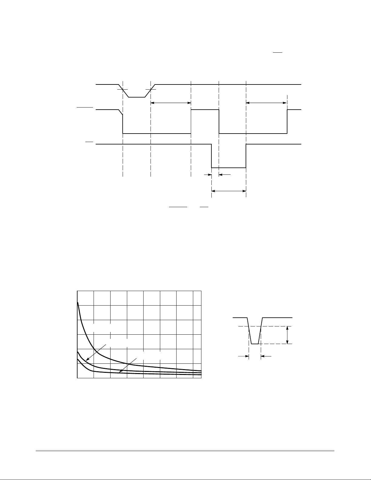
Microprocessor Reset
To generate a processor reset, the manual Reset input
allows different reset sources. A pushbutton switch can be
V
CC
RESET
MR
V
TH
V
TH
t
RP
Figure 12. RESET and MR Timing
one of these. It is effectively debounced by the 1.0 ms
minimum reset pulse width. As MR is TTL/CMOS logic
compatible, it can be driven by an external logic line.
t
RP
t
MD
t
MR
VCC Transient Rejection
The MAX707/708 provides accurate VCC monitoring and
reset timing during power−up, power−down, and
brownout/sag conditions, and rejects negative glitches on
the power supply line. Figure 13 shows the maximum
transient duration vs. maximum negative excursion
300
250
200
V
= 4.90 V
150
100
50
MAXIMUM TRANSIENT DURATION (ms)
TH
V
= 3.08 V
TH
V
= 1.60 V
TH
0
10 90705030 110 130 150
RESET COMPARATOR OVERDRIVE (mV)
Figure 13. Maximum Transient Duration vs.
Overdrive for Glitch Rejection at 255C
(overdrive) for glitch rejection. For a given overdrive, the
point of the curve is the maximum width of the glitch
allowed before the device generates a reset signal. Transient
immunity can be improved by adding a capacitor (100 nF for
example) in close proximity to the VCC pin of the
MAX707/708.
V
CC
V
TH
Overdrive
Duration
http://onsemi.com
6
Page 7
MAX707, MAX708
BUFFERED
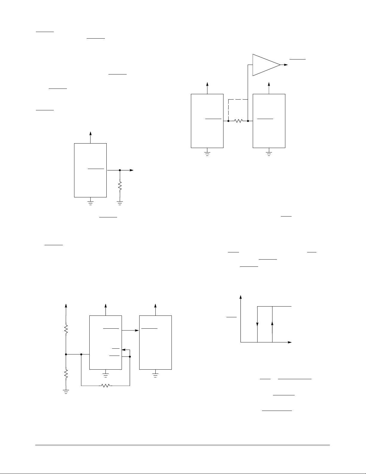
RESET Signal Integrity During Power−Down
The MAX707/708 RESET output is valid until VCC falls
below 1.0 V. Then, the output becomes an open circuit and
no longer sinks current. This means CMOS logic inputs of
the mP will be floating at an undetermined voltage. Most
digital systems are completely shutdown well above this
voltage. However, in the case RESET must be maintained
valid to VCC = 0 V, a pull down resistor must be connected
from RESET to ground to discharge stray capacitances and
hold the output low (Figure 14). This resistor value, though
not critical, should be chosen large enough not to load
RESET and small enough to pull it to ground. R = 100 kW
will be suitable for most applications.
V
CC
MAX707/708
RESET
R
GND
Figure 14. Ensuring RESET Valid to VCC = 0 V
Interfacing with mPs with Bidirectional I/O Pins
100 k
Some mPs have bidirectional reset pins. If, for example,
the RESET output is driven high and the mP wants to put it
low, indeterminate logic level may result. This can be
avoided by adding a 4.7 kW resistor in series with the output
of the MAX707/708 (Figure 15). If there are other
components in the system that require a reset signal, they
should be bu ffered so as not to load the reset line. If the other
components are required to follow the reset I/O of the mP, the
buffer should be connected as shown with the solid line.
BUFFER
V
CC
MAX707/708
GND
Figure 15. Interfacing to Bidirectional Reset I/O
Monitoring Additional Supply Levels
4.7 k
V
CC
m P
RESETRESET
GND
RESET TO
OTHER SYSTEM
COMPONENTS
When connecting a voltage divider to PFI and adjusting it
properly, you can monitor a voltage different than the
unregulated DC one. As shown in Figure 16, to increase
noise immunity, hysteresis may be added to the power−fail
comparator just by a resistor between PFO and PFI. Not to
unbalance the potential divider network, R3 should be 10
times the sum of the two resistors R1 and R2. If required, a
capacitor between PFI and GND will reduce the sensitivity
of the circuit to high−frequency noise on the line being
monitored. The PFO output may be connected to MR input
to generate a low level on the RESET when V
CC
_1
drops out
of tolerance. Thus a RESET is generated when one of the
two voltages is below its threshold level.
V
CC_1
R1
R2
V
CC_2
V
CC
RESET
MAX707/708
PFI
MR
PFO
GND
R3
Figure 16. Monitoring Additional Supply Levels
V
CC_3
V
RESET
m P
GND
CC
http://onsemi.com
7
V
CC_2
PFO
0 V
0 V VLV
V
CC_1
1.25
L
ǒ
R2
R1 V
+
VL+ 1.25 ) R1
VH+ 1.25 (1 ) R1
V
+ VH* V
HYS
H
1.25 * V
)
R2) R3
ǒ
R2 R3
cc_2
R3
R3
Ǔ
cc_2
)
Ǔ
Page 8

MAX707, MAX708
ORDERING INFORMATION
Device Marking Reset VCC Threshold
(V)
MAX707ESA−T S707 4.63 SOIC−8 2500 Tape & Reel
MAX707ESA−TG S707 4.63 SOIC−8
MAX708ESA−T S708 4.38 SOIC−8 2500 Tape & Reel
MAX708ESA−TG S708 4.38 SOIC−8
MAX708RESA−T S708R 2.63 SOIC−8 2500 Tape & Reel
MAX708RESA−TG S708R 2.63 SOIC−8
MAX708SESA−T S708S 2.93 SOIC−8 2500 Tape & Reel
MAX708SESA−TG S708S 2.93 SOIC−8
MAX708TESA−T S708T 3.08 SOIC−8 2500 Tape & Reel
MAX708TESA−TG S708T 3.08 SOIC−8
MAX707CUA−T SAC 4.63 Micro8 4000 Tape & Reel
MAX707CUA−TG SAC 4.63 Micro8
MAX708CUA−T SAD 4.38 Micro8 4000 Tape & Reel
MAX708CUA−TG SAD 4.38 Micro8
MAX708RCUA−T SAG 2.63 Micro8 4000 Tape & Reel
MAX708RCUA−TG SAG 2.63 Micro8
MAX708SCUA−T SAF 2.93 Micro8 4000 Tape & Reel
MAX708SCUA−TG SAF 2.93 Micro8
MAX708TCUA−T SAE 3.08 Micro8 4000 Tape & Reel
MAX708TCUA−TG SAE 3.08 Micro8
†For information on tape and reel specifications,including part orientation and tape sizes, please refer to our Tape and Reel Packaging
Specifications Brochure, BRD8011/D.
Package Shipping
2500 Tape & Reel
(Pb−Free)
2500 Tape & Reel
(Pb−Free)
2500 Tape & Reel
(Pb−Free)
2500 Tape & Reel
(Pb−Free)
2500 Tape & Reel
(Pb−Free)
4000 Tape & Reel
(Pb−Free)
4000 Tape & Reel
(Pb−Free)
4000 Tape & Reel
(Pb−Free)
4000 Tape & Reel
(Pb−Free)
4000 Tape & Reel
(Pb−Free)
†
Micro8 is a trademark of International Rectifier.
http://onsemi.com
8
Page 9

MECHANICAL CASE OUTLINE
PACKAGE DIMENSIONS
8
1
SCALE 1:1
−Y−
−Z−
−X−
A
58
B
1
4
G
H
D
0.25 (0.010) Z
M
SOLDERING FOOTPRINT*
7.0
0.275
S
Y
0.25 (0.010)
C
SEATING
PLANE
SXS
0.10 (0.004)
1.52
0.060
4.0
0.155
CASE 751−07
M
M
Y
N
SOIC−8 NB
ISSUE AK
K
X 45
_
M
J
MARKING DIAGRAM*
8
XXXXX
ALYWX
1
XXXXX = Specific Device Code
A = Assembly Location
L = Wafer Lot
Y = Year
W = Work Week
G = Pb−Free Package
8
XXXXX
ALYWX
G
1
IC
IC
(Pb−Free)
DATE 16 FEB 2011
NOTES:
1. DIMENSIONING AND TOLERANCING PER
ANSI Y14.5M, 1982.
2. CONTROLLING DIMENSION: MILLIMETER.
3. DIMENSION A AND B DO NOT INCLUDE
MOLD PROTRUSION.
4. MAXIMUM MOLD PROTRUSION 0.15 (0.006)
PER SIDE.
5. DIMENSION D DOES NOT INCLUDE DAMBAR
PROTRUSION. ALLOWABLE DAMBAR
PROTRUSION SHALL BE 0.127 (0.005) TOTAL
IN EXCESS OF THE D DIMENSION AT
MAXIMUM MATERIAL CONDITION.
6. 751−01 THRU 751−06 ARE OBSOLETE. NEW
STANDARD IS 751−07.
MILLIMETERS
DIMAMIN MAX MIN MAX
4.80 5.00 0.189 0.197
B 3.80 4.00 0.150 0.157
C 1.35 1.75 0.053 0.069
D 0.33 0.51 0.013 0.020
G 1.27 BSC 0.050 BSC
H 0.10 0.25 0.004 0.010
J 0.19 0.25 0.007 0.010
K 0.40 1.27 0.016 0.050
M 0 8 0 8
____
N 0.25 0.50 0.010 0.020
S 5.80 6.20 0.228 0.244
INCHES
GENERIC
8
XXXXXX
AYWW
1
Discrete
XXXXXX = Specific Device Code
A = Assembly Location
Y = Year
WW = Work Week
G = Pb−Free Package
8
XXXXXX
AYWW
1
Discrete
(Pb−Free)
G
0.6
0.024
1.270
0.050
SCALE 6:1
ǒ
inches
mm
Ǔ
*This information is generic. Please refer to
device data sheet for actual part marking.
Pb−Free indicator, “G” or microdot “G”, may
or may not be present. Some products may
not follow the Generic Marking.
*For additional information on our Pb−Free strategy and soldering
details, please download the ON Semiconductor Soldering and
Mounting Techniques Reference Manual, SOLDERRM/D.
STYLES ON PAGE 2
DOCUMENT NUMBER:
DESCRIPTION:
ON Semiconductor and are trademarks of Semiconductor Components Industries, LLC dba ON Semiconductor or its subsidiaries in the United States and/or other countries.
ON Semiconductor reserves the right to make changes without further notice to any products herein. ON Semiconductor makes no warranty, representation or guarantee regarding
the suitability of its products for any particular purpose, nor does ON Semiconductor assume any liability arising out of the application or use of any product or circuit, and specifically
disclaims any and all liability, including without limitation special, consequential or incidental damages. ON Semiconductor does not convey any license under its patent rights nor the
rights of others.
© Semiconductor Components Industries, LLC, 2019
98ASB42564B
SOIC−8 NB
Electronic versions are uncontrolled except when accessed directly from the Document Repository.
Printed versions are uncontrolled except when stamped “CONTROLLED COPY” in red.
PAGE 1 OF 2
www.onsemi.com
Page 10

STYLE 1:
PIN 1. EMITTER
2. COLLECTOR
3. COLLECTOR
4. EMITTER
5. EMITTER
6. BASE
7. BASE
8. EMITTER
STYLE 5:
PIN 1. DRAIN
2. DRAIN
3. DRAIN
4. DRAIN
5. GATE
6. GATE
7. SOURCE
8. SOURCE
STYLE 9:
PIN 1. EMITTER, COMMON
2. COLLECTOR, DIE #1
3. COLLECTOR, DIE #2
4. EMITTER, COMMON
5. EMITTER, COMMON
6. BASE, DIE #2
7. BASE, DIE #1
8. EMITTER, COMMON
STYLE 13:
PIN 1. N.C.
2. SOURCE
3. SOURCE
4. GATE
5. DRAIN
6. DRAIN
7. DRAIN
8. DRAIN
STYLE 17:
PIN 1. VCC
2. V2OUT
3. V1OUT
4. TXE
5. RXE
6. VEE
7. GND
8. ACC
STYLE 21:
PIN 1. CATHODE 1
2. CATHODE 2
3. CATHODE 3
4. CATHODE 4
5. CATHODE 5
6. COMMON ANODE
7. COMMON ANODE
8. CATHODE 6
STYLE 25:
PIN 1. VIN
2. N/C
3. REXT
4. GND
5. IOUT
6. IOUT
7. IOUT
8. IOUT
STYLE 29:
PIN 1. BASE, DIE #1
2. EMITTER, #1
3. BASE, #2
4. EMITTER, #2
5. COLLECTOR, #2
6. COLLECTOR, #2
7. COLLECTOR, #1
8. COLLECTOR, #1
STYLE 2:
PIN 1. COLLECTOR, DIE, #1
2. COLLECTOR, #1
3. COLLECTOR, #2
4. COLLECTOR, #2
5. BASE, #2
6. EMITTER, #2
7. BASE, #1
8. EMITTER, #1
STYLE 6:
PIN 1. SOURCE
2. DRAIN
3. DRAIN
4. SOURCE
5. SOURCE
6. GATE
7. GATE
8. SOURCE
STYLE 10:
PIN 1. GROUND
2. BIAS 1
3. OUTPUT
4. GROUND
5. GROUND
6. BIAS 2
7. INPUT
8. GROUND
STYLE 14:
PIN 1. N−SOURCE
2. N−GATE
3. P−SOURCE
4. P−GATE
5. P−DRAIN
6. P−DRAIN
7. N−DRAIN
8. N−DRAIN
STYLE 18:
PIN 1. ANODE
2. ANODE
3. SOURCE
4. GATE
5. DRAIN
6. DRAIN
7. CATHODE
8. CATHODE
STYLE 22:
PIN 1. I/O LINE 1
2. COMMON CATHODE/VCC
3. COMMON CATHODE/VCC
4. I/O LINE 3
5. COMMON ANODE/GND
6. I/O LINE 4
7. I/O LINE 5
8. COMMON ANODE/GND
STYLE 26:
PIN 1. GND
2. dv/dt
3. ENABLE
4. ILIMIT
5. SOURCE
6. SOURCE
7. SOURCE
8. VCC
STYLE 30:
PIN 1. DRAIN 1
2. DRAIN 1
3. GATE 2
4. SOURCE 2
5. SOURCE 1/DRAIN 2
6. SOURCE 1/DRAIN 2
7. SOURCE 1/DRAIN 2
8. GATE 1
SOIC−8 NB
CASE 751−07
ISSUE AK
STYLE 3:
STYLE 7:
STYLE 11:
STYLE 15:
PIN 1. DRAIN, DIE #1
2. DRAIN, #1
3. DRAIN, #2
4. DRAIN, #2
5. GATE, #2
6. SOURCE, #2
7. GATE, #1
8. SOURCE, #1
PIN 1. INPUT
2. EXTERNAL BYPASS
3. THIRD STAGE SOURCE
4. GROUND
5. DRAIN
6. GATE 3
7. SECOND STAGE Vd
8. FIRST STAGE Vd
PIN 1. SOURCE 1
2. GATE 1
3. SOURCE 2
4. GATE 2
5. DRAIN 2
6. DRAIN 2
7. DRAIN 1
8. DRAIN 1
PIN 1. ANODE 1
2. ANODE 1
3. ANODE 1
4. ANODE 1
5. CATHODE, COMMON
6. CATHODE, COMMON
7. CATHODE, COMMON
8. CATHODE, COMMON
STYLE 19:
PIN 1. SOURCE 1
2. GATE 1
3. SOURCE 2
4. GATE 2
5. DRAIN 2
6. MIRROR 2
7. DRAIN 1
8. MIRROR 1
STYLE 23:
PIN 1. LINE 1 IN
2. COMMON ANODE/GND
3. COMMON ANODE/GND
4. LINE 2 IN
5. LINE 2 OUT
6. COMMON ANODE/GND
7. COMMON ANODE/GND
8. LINE 1 OUT
STYLE 27:
PIN 1. ILIMIT
2. OVLO
3. UVLO
4. INPUT+
5. SOURCE
6. SOURCE
7. SOURCE
8. DRAIN
DATE 16 FEB 2011
STYLE 4:
PIN 1. ANODE
2. ANODE
3. ANODE
4. ANODE
5. ANODE
6. ANODE
7. ANODE
8. COMMON CATHODE
STYLE 8:
PIN 1. COLLECTOR, DIE #1
2. BASE, #1
3. BASE, #2
4. COLLECTOR, #2
5. COLLECTOR, #2
6. EMITTER, #2
7. EMITTER, #1
8. COLLECTOR, #1
STYLE 12:
PIN 1. SOURCE
2. SOURCE
3. SOURCE
4. GATE
5. DRAIN
6. DRAIN
7. DRAIN
8. DRAIN
STYLE 16:
PIN 1. EMITTER, DIE #1
2. BASE, DIE #1
3. EMITTER, DIE #2
4. BASE, DIE #2
5. COLLECTOR, DIE #2
6. COLLECTOR, DIE #2
7. COLLECTOR, DIE #1
8. COLLECTOR, DIE #1
STYLE 20:
PIN 1. SOURCE (N)
2. GATE (N)
3. SOURCE (P)
4. GATE (P)
5. DRAIN
6. DRAIN
7. DRAIN
8. DRAIN
STYLE 24:
PIN 1. BASE
2. EMITTER
3. COLLECTOR/ANODE
4. COLLECTOR/ANODE
5. CATHODE
6. CATHODE
7. COLLECTOR/ANODE
8. COLLECTOR/ANODE
STYLE 28:
PIN 1. SW_TO_GND
2. DASIC_OFF
3. DASIC_SW_DET
4. GND
5. V_MON
6. VBULK
7. VBULK
8. VIN
DOCUMENT NUMBER:
DESCRIPTION:
ON Semiconductor and are trademarks of Semiconductor Components Industries, LLC dba ON Semiconductor or its subsidiaries in the United States and/or other countries.
ON Semiconductor reserves the right to make changes without further notice to any products herein. ON Semiconductor makes no warranty, representation or guarantee regarding
the suitability of its products for any particular purpose, nor does ON Semiconductor assume any liability arising out of the application or use of any product or circuit, and specifically
disclaims any and all liability, including without limitation special, consequential or incidental damages. ON Semiconductor does not convey any license under its patent rights nor the
rights of others.
© Semiconductor Components Industries, LLC, 2019
98ASB42564B
SOIC−8 NB
Electronic versions are uncontrolled except when accessed directly from the Document Repository.
Printed versions are uncontrolled except when stamped “CONTROLLED COPY” in red.
PAGE 2 OF 2
www.onsemi.com
Page 11
MECHANICAL CASE OUTLINE
PACKAGE DIMENSIONS
SCALE 2:1
Micro8
CASE 846A−02
ISSUE K
DATE 16 JUL 2020
GENERIC
MARKING DIAGRAM*
8
XXXX
AYW G
G
1
XXXX = Specific Device Code
A = Assembly Location
Y = Year
W = Work Week
G = Pb−Free Package
(Note: Microdot may be in either location)
*This information is generic. Please refer to
device data sheet for actual part marking.
Pb−Free indicator, “G” or microdot “G”, may
or may not be present. Some products may
not follow the Generic Marking.
STYLE 1:
PIN 1. SOURCE
2. SOURCE
3. SOURCE
4. GATE
5. DRAIN
6. DRAIN
7. DRAIN
8. DRAIN
STYLE 2:
PIN 1. SOURCE 1
2. GATE 1
3. SOURCE 2
4. GATE 2
5. DRAIN 2
6. DRAIN 2
7. DRAIN 1
8. DRAIN 1
STYLE 3:
PIN 1. N-SOURCE
2. N-GATE
3. P-SOURCE
4. P-GATE
5. P-DRAIN
6. P-DRAIN
7. N-DRAIN
8. N-DRAIN
DOCUMENT NUMBER:
DESCRIPTION:
ON Semiconductor and are trademarks of Semiconductor Components Industries, LLC dba ON Semiconductor or its subsidiaries in the United States and/or other countries.
ON Semiconductor reserves the right to make changes without further notice to any products herein. ON Semiconductor makes no warranty, representation or guarantee regarding
the suitability of its products for any particular purpose, nor does ON Semiconductor assume any liability arising out of the application or use of any product or circuit, and specifically
disclaims any and all liability, including without limitation special, consequential or incidental damages. ON Semiconductor does not convey any license under its patent rights nor the
rights of others.
© Semiconductor Components Industries, LLC, 2019
98ASB14087C
MICRO8
Electronic versions are uncontrolled except when accessed directly from the Document Repository.
Printed versions are uncontrolled except when stamped “CONTROLLED COPY” in red.
PAGE 1 OF 1
www.onsemi.com
Page 12

ON Semiconductor and are trademarks of Semiconductor Components Industries, LLC dba ON Semiconductor or its subsidiaries in the United States and/or other countries.
ON Semiconductor owns the rights to a number of patents, trademarks, copyrights, trade secrets, and other intellectual property. A listing of ON Semiconductor’s product/patent
coverage may be accessed at www.onsemi.com/site/pdf/Patent−Marking.pdf
ON Semiconductor makes no warranty, representation or guarantee regarding the suitability of its products for any particular purpose, nor does ON Semiconductor assume any liability
arising out of the application or use of any product or circuit, and specifically disclaims any and all liability, including without limitation special, consequential or incidental damages.
Buyer is responsible for its products and applications using ON Semiconductor products, including compliance with all laws, regulations and safety requirements or standards,
regardless of any support or applications information provided by ON Semiconductor. “Typical” parameters which may be provided in ON Semiconductor data sheets and/or
specifications can and do vary in different applications and actual performance may vary over time. All operating parameters, including “Typicals” must be validated for each customer
application by customer’s technical experts. ON Semiconductor does not convey any license under its patent rights nor the rights of others. ON Semiconductor products are not
designed, intended, or authorized for use as a critical component in life support systems or any FDA Class 3 medical devices or medical devices with a same or similar classification
in a foreign jurisdiction or any devices intended for implantation in the human body. Should Buyer purchase or use ON Semiconductor products for any such unintended or unauthorized
application, Buyer shall indemnify and hold ON Semiconductor and its officers, employees, subsidiaries, affiliates, and distributors harmless against all claims, costs, damages, and
expenses, and reasonable attorney fees arising out of, directly or indirectly, any claim of personal injury or death associated with such unintended or unauthorized use, even if such
claim alleges that ON Semiconductor was negligent regarding the design or manufacture of the part. ON Semiconductor is an Equal Opportunity/Affirmative Action Employer. This
literature is subject to all applicable copyright laws and is not for resale in any manner.
. ON Semiconductor reserves the right to make changes without further notice to any products herein.
PUBLICATION ORDERING INFORMATION
LITERATURE FULFILLMENT:
Email Requests to: orderlit@onsemi.com
ON Semiconductor Website: www.onsemi.com
TECHNICAL SUPPORT
North American Technical Support:
Voice Mail: 1 800−282−9855 Toll Free USA/Canada
Phone: 011 421 33 790 2910
Europe, Middle East and Africa Technical Support:
Phone: 00421 33 790 2910
For additional information, please contact your local Sales Representative
◊
www.onsemi.com
1
 Loading...