

ON Semiconductor LV8731V User Manual
PWM Constant-Current
Control Stepper Motor
Driver
Monolithic Linear IC
LV8731V
Overview
The LV8731V is a 2−channel H−bridge driver IC that can switch a
stepper motor driver, which supports micro−step drive with 1/16−step
resolution, and two channels of a brushed motor driver, which
supports forward, reverse, brake, and standby of a motor. It is ideally
suited for driving brushed DC motors and stepper motors used in
office equipment and amusement applications.
Function
• Single−channel PWM Current Control Stepper Motor Driver
(Selectable with DC Motor Driver Channel 2) Incorporated
• BiCDMOS Process IC
• Low on Resistance (Upper Side: 0.3 ; Lower Side: 0.25 ;
Total of Upper and Lower: 0.55 ; T
= 25°C, I
A
• Micro−step Mode can be Set to Full−step, Half−step, Quarter−step, or
1/16−step
• Excitation Step Proceeds Only by Step Signal Input
• Motor Current Selectable in Four Steps
• Output Short−circuit Protection Circuit (Selectable from Latch−type
or Auto−reset−type) Incorporated
• Unusual Condition Warning Output Pins
• No Control Power Supply Required
= 2 A)
O
www.onsemi.com
SSOP44K
CASE 940AF
MARKING DIAGRAM
LV8731
YMWL
Y = Year of Production, Last Number
M = Assembly Operation Month
WL = Wafer Lot Number
© Semiconductor Components Industries, LLC, 2013
February, 2021 − Rev. 6
ORDERING INFORMATION
See detailed ordering and shipping information in the package
dimensions section on page 26 of this data sheet.
1 Publication Order Number:
LV8731V/D
LV8731V
SPECIFICATIONS
ABSOLUTE MAXIMUM RATINGS at T
= 25°C
A
Parameter Symbol Conditions Ratings Unit
Supply Voltage VM max VM, VM1, VM2 36 V
Output Peak Current IO peak Tw ≤ 10 ms, duty 20%, Per 1ch 2.5 A
Output Current IO max Per 1ch 2 A
Logic Input Voltage V
IN
ATT1, ATT2, EMM, RST/BLK, STEP/DC22,
FR/DC21, MD2/DC12, MD1/DC11, DM, OE, ST
−0.3 to +6 V
MONI/EMO Input Voltage Vmoni/Vemo −0.3 to +6 V
Allowable Power Dissipation Pd max (Note 1) 3.25 W
Operating Temperature Topr −40 to +85 °C
Storage Temperature Tstg −55 to +150 °C
Stresses exceeding those listed in the Maximum Ratings table may damage the device. If any of these limits are exceeded, device functionality
should not be assumed, damage may occur and reliability may be affected.
1. Specified circuit board : 90.0 mm × 90.0 mm × 1.6 mm, glass epoxy 2−layer board, with backside mounting.
2. Caution 1: Absolute maximum ratings represent the value which cannot be exceeded for any length of time.
3. Caution 2: Even when the device is used within the range of absolute maximum ratings, as a result of continuous usage under high
temperature, high current, high voltage, or drastic temperature change, the reliability of the IC may be degraded. Please contact us for the
further details.
ALLOWABLE OPERATING RATINGS T
= 25°C
A
Parameter Symbol Conditions Ratings Unit
Supply Voltage Range VM VM, VM1, VM2 8 to 32 V
Logic Input Voltage V
IN
ATT1, ATT2, EMM, RST/BLK, STEP/DC22,
0 to 5.5 V
FR/DC21, MD2/DC12, MD1/DC11, DM, OE, ST
VREF Input Voltage Range VREF 0 to 3 V
Functional operation above the stresses listed in the Recommended Operating Ranges is not implied. Extended exposure to stresses beyond
the Recommended Operating Ranges limits may affect device reliability.
ELECTRICAL CHARACTERISTICS T
= 25°C, VM = 24 V, VREF = 1.5 V
A
Ratings
Parameter
Symbol Conditions
Min Typ Max
Unit
Standby Mode Current Drain IMstn ST = “L”, I(VM) + I(VM1) + I(VM2) 100 400
Current Drain IM ST = “H”, OE = “L”, with no load
3.2 5 mA
I(VM) + I(VM1) + I(VM2)
VREG5 Output Voltage Vreg5 IO = −1 mA 4.5 5 5.5 V
Thermal Shutdown Temperature TSD Design guarantee 150 180 200 °C
Thermal Hysteresis Width
TSD
Design guarantee 40 °C
MOTOR DRIVER
Output On Resistance
Ronu IO = 2 A, Upper−side on resistance 0.3 0.4
Rond IO = 2 A, Lower−side on resistance 0.25 0.33
Output Leakage Current IOleak 50
Diode Forward Voltage VD ID = −2 A 1.2 1.4 V
Logic Pin Input Current
IINL ATT1, ATT2, EMM, RST/BLK,
4 8 12
STEP/DC22, FR/DC21, MD2/DC12,
MD1/DC11, DM, OE, ST,
= 0.8 V
V
IN
IINH VIN = 5 V 30 50 70
A
A
A
A
www.onsemi.com
2
LV8731V
ELECTRICAL CHARACTERISTICS (continued) T
Parameter Unit
Logic Input Voltage
Current Setting Comparator
Threshold Voltage
(Current Step Switching)
Current Setting Comparator Threshold
Voltage (Current Attenuation Rate Switching)
Chopping Frequency Fchop Cchop = 200 pF 40 50 60 kHz
CHOP Pin Charge/Discharge Current Ichop 7 10 13
Chopping Oscillation Circuit Threshold
Voltage
VREF Pin Input Current Iref VREF = 1.5 V −0.5
MONI Pin Saturation Voltage Vsatmon Imoni = 1 mA 400 mV
CHARGE PUMP
VG Output Voltage
Rise Time tONG VG = 0.1 mF, Between CP1−CP2
Oscillator Frequency Fosc 90 125 150 kHz
High VINh
Low VINl 0 0.8 V
1/16 step
resolution
Quarter step
resolution
Half step
resolution
Full step
resolution
= 25°C, VM = 24 V, VREF = 1.5 V
A
Ratings
ConditionsSymbol
ATT1, ATT2, EMM, RST/BLK,
STEP/DC22, FR/DC21, MD2/DC12,
MD1/DC11, DM, OE, ST
Vtdac0_4W Step 0 (When initialized: channel 1
comparator level)
Vtdac1_4W Step 1 (Initial state + 1) 0.291 0.3 0.309 V
Vtdac2_4W Step 2 (Initial state + 2) 0.285 0.294 0.303 V
Vtdac3_4W Step 3 (Initial state + 3) 0.279 0.288 0.297 V
Vtdac4_4W Step 4 (Initial state + 4) 0.267 0.276 0.285 V
Vtdac5_4W Step 5 (Initial state + 5) 0.255 0.264 0.273 V
Vtdac6_4W Step 6 (Initial state + 6) 0.240 0.249 0.258 V
Vtdac7_4W Step 7 (Initial state + 7) 0.222 0.231 0.240 V
Vtdac8_4W Step 8 (Initial state + 8) 0.201 0.21 0.219 V
Vtdac9_4W Step 9 (Initial state + 9) 0.180 0.189 0.198 V
Vtdac10_4W Step 10 (Initial state + 10) 0.157 0.165 0.173 V
Vtdac11_4W Step 11 (Initial state + 11) 0.134 0.141 0.148 V
Vtdac12_4W Step 12 (Initial state + 12) 0.107 0.114 0.121 V
Vtdac13_4W Step 13 (Initial state + 13) 0.080 0.087 0.094 V
Vtdac14_4W Step 14 (Initial state + 14) 0.053 0.06 0.067 V
Vtdac15_4W Step 15 (Initial state + 15) 0.023 0.03 0.037 V
Vtdac0_W Step 0 (When initialized : channel 1
comparator level)
Vtdac4_W Step 4 (Initial state + 1) 0.267 0.276 0.285 V
Vtdac8_W Step 8 (Initial state + 2) 0.201 0.21 0.219 V
Vtdac12_W Step 12 (Initial state + 3) 0.107 0.114 0.121 V
Vtdac0_H Step 0 (When initialized : channel 1
comparator level)
Vtdac8_H Step 8 (Initial state + 1) 0.201 0.21 0.219 V
Vtdac8_F Step 8’ (When initialized : channel 1
comparator level)
Vtatt00 ATT1 = L, ATT2 = L 0.291 0.3 0.309 V
Vtatt01 ATT1 = H, ATT2 = L 0.232 0.24 0.248 V
Vtatt10 ATT1 = L, ATT2 = H 0.143 0.15 0.157 V
Vtatt11 ATT1 = H, ATT2 = H 0.053 0.06 0.067 V
Vtup 0.8 1 1.2 V
Vtdown 0.4 0.5 0.6 V
VG 28 28.7 29.8 V
0.1 F
ST = “H” →VG = VM + 4 V
2.0 5.5 V
0.291 0.3 0.309 V
0.291 0.3 0.309 V
0.291 0.3 0.309 V
0.291 0.3 0.309 V
200 500
MaxTypMin
A
A
S
www.onsemi.com
3
LV8731V
ELECTRICAL CHARACTERISTICS (continued) T
Parameter Unit
OUTPUT SHORT−CIRCUIT PROTECTION
EMO Pin Saturation Voltage
CEM Pin Charge Current Icem Vcem = 0 V 7 10 13
CEM Pin Threshold Voltage Vtcem 0.8 1 1.2 V
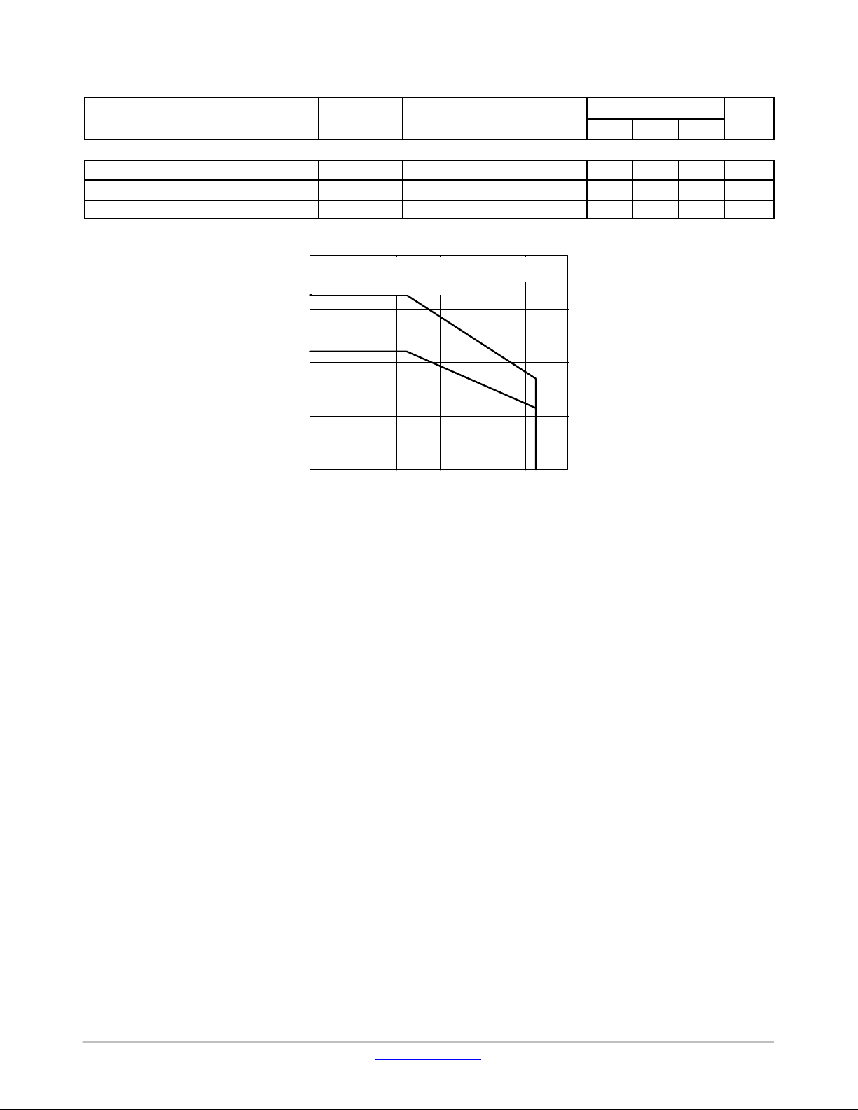
4.0
*1 With components mounted on the exposed die−pad board
*2 With no components mounted on the exposed die−pad board
Two−layer circuit board 1 *1
3.25
3.0
Two−layer circuit board 2 *2
2.20
2.0
1.0
Allowable power dissipation, Pd max − W
0
−20 0 20 40 60 80 100
= 25°C, VM = 24 V, VREF = 1.5 V
A
Ratings
ConditionsSymbol
Vsatemo Iemo = 1 mA 400 mV
Pd max − T
Ambient temperature, TA − °C
A
1.69
1.14
MaxTypMin
Figure 1. Power Dissipation vs Ambient Temperature Characteristic
A
www.onsemi.com
4
LV8731V
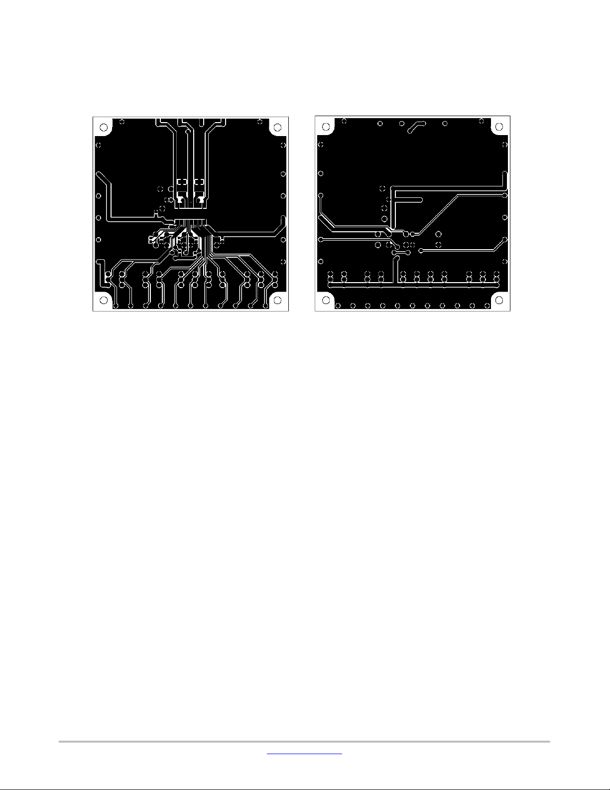
Substrate Specifications (Substrate recommended for operation of LV8731V)
Size: 90 mm × 90 mm × 1.6 mm (two−layer substrate [2S0P])
Material: Glass epoxy
Copper wiring density: L1 = 85% / L2 = 90%
Figure 2. L1: Copper Wiring Pattern Diagram Figure 3. L2: Copper Wiring Pattern Diagram
Cautions
1. The data for the case with the Exposed Die−Pad
substrate mounted shows the values when 90% or
more of the Exposed Die−Pad is wet
2. For the set design, employ the derating design with
sufficient margin.
Stresses to be derated include the voltage, current,
junction temperature, power loss, and mechanical
stresses such as vibration, impact, and tension.
Accordingly, the design must ensure these stresses
to be as low or small as possible.
The guideline for ordinary derating is shown
below :
(1) Maximum value 80% or less for the voltage
rating
(2) Maximum value 80% or less for the current
rating
(3) Maximum value 80% or less for the
temperature rating
3. After the set design, be sure to verify the design
with the actual product.
Confirm the solder joint state and verify also the
reliability of solder joint for the Exposed Die−Pad,
etc.
Any void or deterioration, if observed in the solder
joint of these parts, causes deteriorated thermal
conduction, possibly resulting in thermal
destruction of IC
www.onsemi.com
5
LV8731V
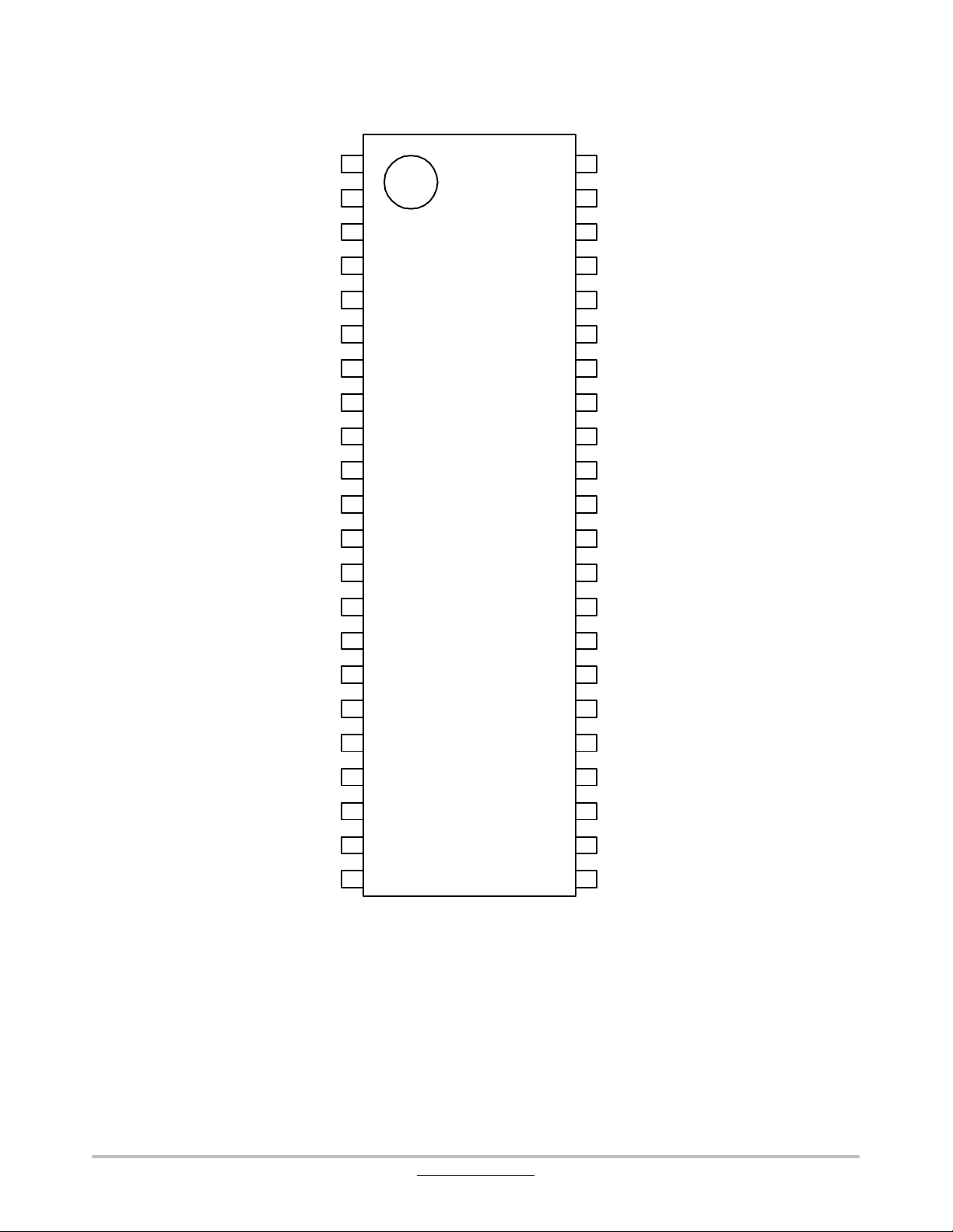
PIN ASSIGNMENT
VG
VM
CP2
CP1
VREG5
ATT2
ATT1
EMO
CEM
EMM
CHOP
MONI
RST/BLK
STEP/DC22
10
11
12
13
14
1
2
3
4
5
6
7
8
9
LV8731V
44
43
42
41
40
39
38
37
36
35
34
33
32
31
OUT1A
OUT1A
PGND
NC
NC
VM1
VM1
RF1
RF1
OUT1B
OUT1B
OUT2A
OUT2A
RF2
FR/DC21
MD2/DC12
MD1/DC11
DM
OE
ST
VREF
GND
15
16
17
18
19
20
21
22
Top View
Figure 4. Pin Assignment
30
29
28
27
26
25
24
23
RF2
VM2
VM2
NC
NC
PGND
OUT2B
OUT2B
www.onsemi.com
6
LV8731V
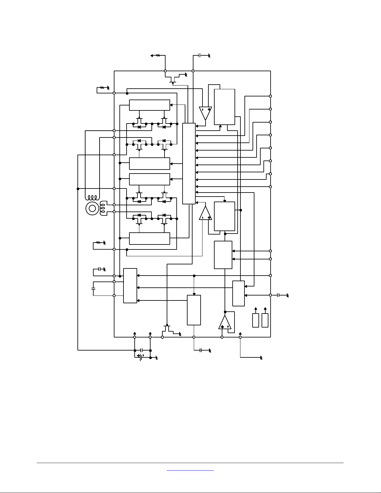
BLOCK DIAGRAM
RF2OUT2BOUT2AVM2
VM
OUTBOUTARFVGCFCP2
Output Preamplifier
Stage
Output Preamplifier
Stage
Output Preamplifier
Stage
Output Preamplifier
Stage
EMO
CEM
Current
(4W1−2/
selection
Output Control Logic
Current
(4W1−2/
selection
W1−2/1−2/2)
W1−2/1−2/2)
OE DM EMM
BLK
RST/
DC22
STEP
FR/
DC21
MD2/
DC12
DC11
Charge Pump
VM
Regulator
MONI
PGND
VREG5
Figure 5. Block Diagram
(4 levels
Attenuator
selectable)
Oscillation
VREF
Circuit
GND
TSD
CHOP ST ATT1 ATT2 MD1/
LVS
www.onsemi.com
7
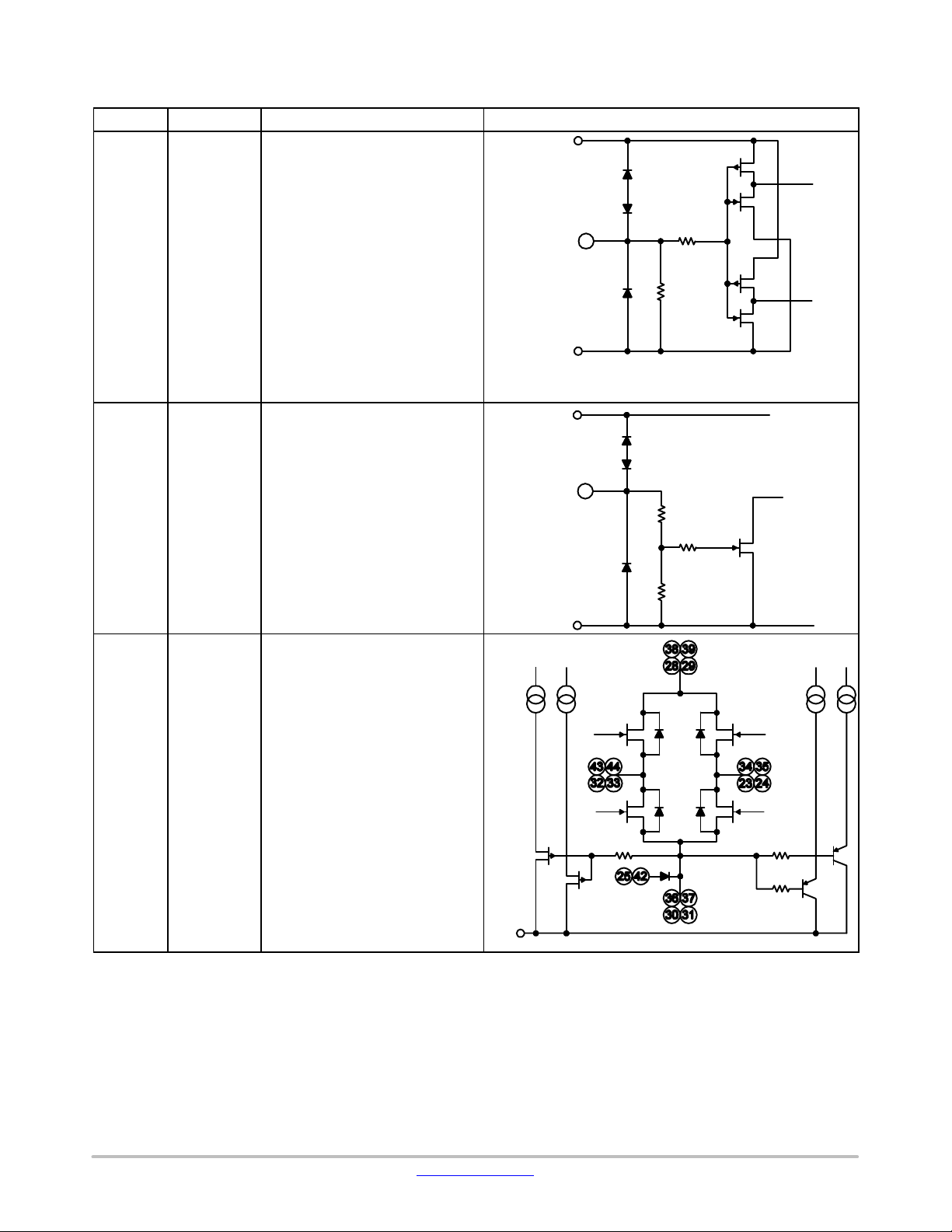
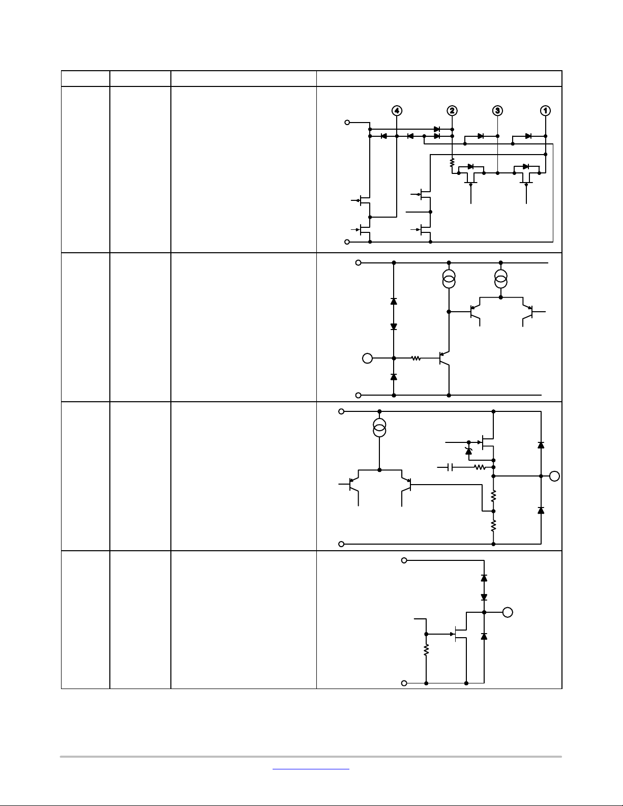
PIN FUNCTIONS
Pin No.
6
7
10
13
14
15
16
17
18
19
20 ST Chip enable pin
Pin Name Pin Function Equivalent Circuit
ATT2
ATT1
EMM
RST/BLK
STEP/DC22
FR/DC21
MD2/DC12
MD1/DC11
DM
OE
Motor holding current switching pin
Motor holding current switching pin
Output short−circuit protection mode
switching pin
RESET input pin (STM) / Blanking time
switching pin (DCM)
STEP signal input pin (STM) / Channel
2 output control input pin 2 (DCM)
CW / CCW signal input pin (STM) /
Channel 2 output control input pin 1
(DCM)
Excitation mode switching pin 2 (STM)
/ Channel 1 output control input pin 2
(DCM)
Excitation mode switching pin 1 (STM)
/ Channel 1 output control input pin 1
(DCM)
Drive mode (STM/DCM) switching pin
Output enable signal input pin
LV8731V
VREG5
10 k
100 k
GND
VREG5
23, 24
25, 42
28, 29
30, 31
32, 33
34, 35
36, 37
38, 39
43, 44
OUT2B
PGND
VM2
RF2
OUT2A
OUT1B
RF1
VM1
OUT1A
Channel 2 OUTB output pin
Power system ground
Channel 2 motor power supply
connection pin
Channel 2 current−sense resistor connection pin
Channel 2 OUTA output pin
Channel 1 OUTB output pin
Channel 1 current−sense resistor
connection pin
Channel 1 motor power supply pin
Channel 1 OUTA output pin
GND
GND
10 k
20 k
10 k
80 k
500
500
www.onsemi.com
8
PIN FUNCTIONS (continued)
Pin No. Equivalent CircuitPin FunctionPin Name
1
2
3
4
VG
VM
CP2
CP1
LV8731V
Charge pump capacitor connection pin
Motor power supply connection pin
Charge pump capacitor connection pin
Charge pump capacitor connection pin
VREG5
100
GND
21 VREF Constant current control reference volt-
5 VREG5 Internal power supply capacitor con-
8
12
EMO
MONI
age input pin
nection pin
Output short−circuit state warning
output pin
Position detection monitor pin
VREG5
500
GND
VM
2 k
78 k
26 k
GND
VREG5
www.onsemi.com
9
GND
 Loading...