

Page 1
BLDC Motor Driver,
f
2
Single-Phase, 12 V
Advance Information
LV8314C
INTRODUCTION
Overview
The LV8314C is the driver for 12 V single phase BLDC motor. Its
target output duty−cycle can be set by input PWM duty−cycle. The
output duty−cycle curve setting can be stored to the internal
nonvolatile memory (NVM). In addition, lead−angle can also be
adjusted by the configuration saved in the internal NVM. The internal
NVM can be programmed by a dedicated GUI. Thus, it can drive
various kinds of motors at high efficiency and low noise.
Features
• Selectable Soft Start or Direct Output PWM Duty Control in Start−up
• Single−phase Full Wave Driver with Open-loop Output Duty Control
• Embedded Power FETs, Iomax [peak] = 1.0 A
• PWM Duty−cycle Input (7 kHz to 40 kHz)
• PWM Soft Switching Phase Transition
• Soft Switching Width Adjustment (Rise and Fall Individually)
• Soft PWM Duty−cycle Transitions (Changing the Target Output
Duty−cycle Gradually)
• Built−in Current Limit Function and Over Current Protection
Function
• Built In Thermal Protection Function
• Built−in Locked Rotor Protection and Automatic Recovery Function
• FG Signal Output Frequency Selectable (1 Time, 2 Times or
0.5 Times Hall Input Frequency)
• RD Signal Polarity Selectable
• FG or RD Signal Output Selectable
• Dynamic Lead Angle Adjustment with Respect to Rotation Speed
• Parameter Setting by SPI Communication
• Embedded EEPROM as NVM
• Parameter Setting to the NVM
• These Devices are Pb−Free, Halogen Free/BFR Free and are RoHS
Compliant
Typical Applications
• Circulation Fan in Refrigerator
www.onsemi.com
14
1
TSSOP−14 WB
CASE 948G
MARKING DIAGRAM
14
LV83
14C
ALYW
1
LV8314C = Specific Device Code
A = Assembly Location
L = Wafer Lot
Y = Year
W = Work Week
PIN ASSIGNMENT
1
OUT1
2
PVCC
3
VCC
4
REG
5
VDD
6
IN1
7
IN2 FG
14
RF
13
TSL2
12
OUT
11
GND
10
TSL
9
PWM
8
This document contains information on a new product. Specifications and information
herein are subject to change without notice.
© Semiconductor Components Industries, LLC, 2020
January , 2021 − Rev. P5
1 Publication Order Number:
(Top view)
ORDERING INFORMATION
See detailed ordering and shipping information on page 26 o
this data sheet.
LV8314C/D
Page 2
Application Diagram
Table 1. EXTERNAL COMPONENT VALUE
Device
Qty
Description
Value
Tol
Footprint
Manufacture
Manufacture
D1
1
Anti−reverse connection diode
−
−
D2
1
Anti−abnormal boost Zener diode
−
−
C1
1
VCC bypass capacitor
10 mF / 50 V
10%
C2
1
REG bypass capacitor
1 mF / 25 V
10%
C3
1
Filter of system noise
0.1 mF / 16 V
10%
R1
1
Current limiter resistor for Hall
2 kW/ 1/4 W
5%
R2
1
FG pull−up resistor
10 kW/ 1/4 W
5%
R3
1
Sense resistor for CLM/OCP
200 mW/ ⅛ W
1%
T1
1
Hall element
−
−
Figure 1 shows the application diagram.
Power supply
voltage
D1
D2
( )
R1
T1
C1
C2
( )
C3
OUT1
PVCC
VCC
REG
VDD
IN1
IN2
1
2
3
4
5
6
7
Boot
strap
5 V
Regulator
UVLO
TSD
Hall
Comparator
LV8314C
M
Pre−Driver
Drive Control Logic
OSC
Current
limiter
RF
14
TSL2
13
OUT2
12
GND
11
TSL
10
PWM
9
FG
8
R3
Control (PWM) signal
Pull−up
R2
Rotation signal
Figure 1. Application diagram
The power supplies of the IC need to be decoupled
properly. This means that at least one external capacitor C1
must be connected in between GND and VCC, and one
external capacitor C2 between REG, VDD and GND.
External Components
Table 1 shows the external component list for the
application diagram.
Part Number
www.onsemi.com
2
Page 3
LV8314C
Table 2. TRUTH TABLE
IN1
IN2
Inner PWM State*
OUT1
OUT2
FG
Operation State
On
L
H
Drive mode
Off
LLRegeneration mode
On
H
LLDrive mode
Off
LLRegeneration mode
VCC and GND (VCC, GND)
The power supplies of the IC need to be decoupled
properly. The following three capacitors must be connected.
• Between VCC (pin 3) and ground as C1 in the application
diagram
• Between REG (VDD) and ground as C2
The Zener diode (D2) in Figure 1 is mandatory to prevent
the IC break down in case the supply voltage exceeds the
absolute maximum ratings due to the flyback voltage.
Hall−Sensor Input Pins (IN1, IN2)
Differential output signals of the hall sensor are connected
at IN1 and IN2. It is recommended that the capacitor (C3) is
connected between both pins to filter system noise. The
value of C3 should be selected properly depending on the
system noise. When a Hall IC is used, the output of the Hall
IC must be connected to the IN1 pin and the IN2 pin must be
kept in the middle level of the Hall IC power supply voltage
which should be corresponded to recommended operating
range.
L H
Command Input Pin (PWM)
This pin reads the duty−cycle of the PWM pulse which
controls rotational speed. The PWM input signal level is
supported from 2.8 V to 5.5 V. Linear voltage control is not
supported. The minimum pulse width is 200 ns.
Current Limiter Resistor for Hall (R1)
Hall output amplitude can be adjusted by R1.
The amplitude is proportional to Hall bias level VH for
particular magnetic flux density. VH is determined by the
following equation.
VH + VREG
ǒ
Rh ) R1
Ǔ
(eq. 1)
Rh
Where
VREG: REG pin voltage (5 V)
Rh: Hall resistance
However, it should be considered with Hall sensor
specification and Hall bias current. The bias current should
be set under 10 mA which is REG pin max current.
Hi−Z
H L
*Inner PWM state means the OUTPUT active period decided by inner control logic. Don’t match with PWM−pin input signal.
*Condition: Register “DRVMODE [1:0]” = 01
www.onsemi.com
3
Page 4
LV8314C
Table 3. ABSOLUTE MAXIMUM RATINGS
Parameter
Symbol
Conditions
Ratings
Unit
Maximum supply voltage
VCC
VCC pin
20
V
Maximum output voltage
V
OUT1/OUT2 pin
20
V
Maximum output current (Note 1)
I
OUT1/OUT2 pin
1.0
A
REG pin maximum output current
I
REG pin
10
mA
IN1/IN2 pin maximum input voltage
V
IN1/IN2 pin
5.5
V
PWM pin maximum input voltage
V
PWM pin
5.5
V
FG pin withstanding voltage
V
FG pin
20
V
FG pin maximum current
I
FG pin
7.5
mA
Allowable power dissipation (Note 2)
Pd
0.6
W
Operating temperature
TOP−40 to 105
C
Storage temperature
T
−55 to 150
C
Maximum junction temperature
Tj
150
C
Moisture Sensitivity Level (MSL) (Note 3)
MSL
1
Lead temperature soldering Pb−free versions (30 seconds or less)
T
255
C
ESD Human body Model: HBM (Note 5)
ESD
2500
V
Table 4. THERMAL CHARACTERISTICS
Parameter
Symbol
Value
Unit
Thermal Resistance, Junction−to−Ambient
R
193
C/W
Thermal Resistance, Junction−to−Case (Top)
R
11.6
C/W
SPECIFICATIONS
MAX
OUTMAX
OUTMAX
REGMAX
INMAX
PWMMAX
FGMAX
FGMAX
MAX
STG
MAX
°
°
°
(Note 4)
SLD
HBM
±
°
Stresses exceeding those listed in the Maximum Ratings table may damage the device. If any of these limits are exceeded, device functionality
should not be assumed, damage may occur and reliability may be affected.
1. I
2. Specified circuit board: TBD
is the peak value of the motor supply current.
OUTMAX
3. Moisture Sensitivity Level (MSL): IPC/JEDEC standard: J−STD−020A
4. For information, please refer to our Soldering and Mounting Techniques Reference Manual, SOLDERRM/D
http://www.onsemi.com/pub_link/Collateral/SOLDERRM−D.PDF
5. ESD Human Body Model is based on JEDEC standard: JESD22−A114
q
JA
Y
JT
°
°
Figure 2. Power Dissipation vs. Ambient Temperature Characteristics
www.onsemi.com
4
Page 5
LV8314C
Table 5. RECOMMENDED OPERATING RANGES
Parameter
Symbol
Conditions
Value
Unit
VCC supply voltage
VCC
VCC pin
12
V
VCC operating supply voltage range1 (Note 6)
VCC
VCC pin
3.9 to 5.2
V
VCC operating supply voltage range2
VCC
VCC pin
5.2 to16
V
PWM input frequency range
F
PWM pin
7 to 40
kHz
PWM minimum input low/high pulse width
TW
PWM pin
200
ns
IN1 input voltage range
V
IN1 pin
0 to VDD
V
IN2 input voltage range
V
IN2 pin
0.3 to VDD * 0.6
V
Minimum RF resistor value
R_RFmin
0.20
TYP
OP1
OP2
PWM
PWM
IN1
IN2
W
Functional operation above the stresses listed in the Recommended Operating Ranges is not implied. Extended exposure to stresses beyond
the Recommended Operating Ranges limits may affect device reliability.
6. When the VCC voltage is below 5.2 V, there are possibility to change the electric characteristics due to low VCC. However a motor keeps
rotation until to 3.9 V, normally.
www.onsemi.com
5
Page 6
Electrical Characteristics
Table 6. ELECTRICAL CHARACTERISTICS (TA = 25
C, VCCOP = 12 V unless otherwise noted)
Parameter
Symbol
Conditions
Min
Typ
Max
Unit
Circuit current
ICC−3.35mA
OUT1/OUT2 High−side on−resistance
R
= 0.3 A
−
0.4
0.8
OUT1/OUT2 Low−side on−resistance
R
IO = 0.3 A
−
0.4
0.8
OUT1/OUT2 PWM output frequency
f
−48−
kHz
PWM pin low level input voltage
V
−−0.7
V
PWM pin high level input voltage
V
2.8−−
V
PWM input resolution
−8−
Bit
PWM input bias current
I
VDD = 5.5 V, PWM = 0 V
142843
A
FG pin on−resistance
V
IFG = 5 mA
−−60
FG pin leak current
I
VCC = 16 V, VFG = 16 V
−−1
A
REG pin output voltage
V
4.7
5.0
5.3
V
REG pin output voltage load regulation
V
I
= −10 mA
−−50
mV
Lock−detection time1 (Note 7)
T
Under rotation
0.27
0.3
0.33
s
Lock−detection time2 (Note 8)
T
Start−up/Restart, LOCK_DET = 0
0.63
0.7
0.77
s
Lock−Stop release time1 from 1st to 4th off time
T
3.1
3.5
3.9
s
Lock−Restart on time (Note 8)
T
LOCK_DET = 0
0.63
0.7
0.77
s
Lock−Restart time ratio1 (Note 7)
R
(T
LOCK_DET = 0)
−5−
−
Lock−Stop release time2 as from 5th off time
T
12.51415.5
s
Lock−Restart time ratio2 as from 5th off time
R
(T
LOCK_DET = 0)
−20−
Thermal shutdown protection detection
T
150
180
−°C
Thermal shutdown protection detection
T
−40−°C
Over current detection voltage
I
135
150
165
mV
Current limiter1
I
CL_LVL = 1
657585
mV
Current limiter2
I
CL_LVL = 0
90
100
110
mV
Hall input bias current
I
IN1, IN2 = 0 V
−−1
A
Hall input sensitivity
V
40−−
mV
UVLO detection voltage
V
3.2
3.4
3.6
V
UVLO hysteresis voltage
V
0.1
0.2
0.4
V
LV8314C
°
(Note 8)
(Note 9)
(Note 9)
OH−ONIO
OL−ON
PWMO
PWML
PWMH
D
PWM
pwmin
FGL
FGLK
REG
D
REGLD
LD1
LD2
LRoff1
LRon
LR1
LRoff2
LR2
REG
LRoff1/TLRon,
LRoff2/TLRon,
W
W
m
W
m
D
OVC
D
uvdet
D
TSD
TSD
CL1
CL2
hin
m
hin
uv
temperature
hysteresis
Product parametric performance is indicated in the Electrical Characteristics for the listed test conditions, unless otherwise noted. Product
performance may not be indicated by the Electrical Characteristics if operated under different conditions.
7. When a motor rotates with below 50 rpm (phase change period over 0.3 s), lock protection will works. See Figure 20 for the detail.
8. When a motor can’t rotate for the time which is set by the register named LOCK_DET after start−up, lock protection will work. See Figure 21
for the detail.
9. When the locked rotor state continues for long time, lock stop period changes as from 5th off time. See Figure 21 for the detail.
www.onsemi.com
6
Page 7
Block Diagram
Figure 3 shows the functional block diagram of LV8314C.
OUT1
1
LV8314C
RF
14
PVCC
VCC
REG
VDD
IN1
IN2
2
3
Boot
strap
4
5 V
Regulator
5
6
7
UVLO
TSD
Hall
Comparator
NVM
Pre−Driver
Drive Control Logic
OSC
Current
limiter
Duty
Cycle
Counter
TSL2
13
OUT2
12
GND
11
TSL
10
PWM
9
FG
8
Figure 3. Block Diagram
www.onsemi.com
7
Page 8
Pin Description
Table 7. PIN LIST AND FUNCTION
Pin No.
Pin Name
Description
1
OUT1
Motor drive output pin. This pin is connected to the built−in power MOSFET
2
PVCC
Power supply pin for built−in power MOSFET
3
VCC
Power supply for internal circuit, ex. Pre−driver, charge−pump
4
REG
5.0 V regulator output. This voltage acts as a power source for oscillator, protection circuits, and so on.
5
VDD
Power supply pin for both digital and analog circuits. This pin must be connected to REG pin
6
IN1
7
IN2
8FGThe FG (frequency generator) output controls the motor electrical rotational speed (FG output
9
PWM
Rotational control signal input pin. The rotational speed is controlled by duty−cycle of the pulse and is
10
TSL
Test mode pin. This pin connect to GND typically
11
SGND
Internal circuit ground pin When short to GND, FG pin is serial in/out. When short to REG, PWM pin is
12
OUT2
Motor drive output pin. This pin is connected to the built−in power MOSFET
13
TSL2
Test mode pin. This pin connect to GND typically
14
RF
Sense resistor voltage input for current limit/over current protection
Table 7 shows the pin list and their functions.
The maximum load current of REG is 10 mA. Be sure not to exceed this maximum current
Hall sensor input pin. The differential outputs of the hall sensor need to be connected to IN1 and IN2 each.
synchronizes with the Hall sensor signal). The FG pin is an open drain output. Recommended pull up
resistor is 1 kW to 100 kW. Leave the pin open when not in use. FG pin can be selected from 2 times, 0.5
times FG and RD. switching by bit setting of Reg. 0x0027 “TACHSEL”
proportional to the duty−cycle ratio.
LV8314C
serial in and FG pin is for serial out
NOTE: Characteristic values comply with the conditions in Table 6. “ELECTRICAL CHARACTERISTICS”.
www.onsemi.com
8
Page 9
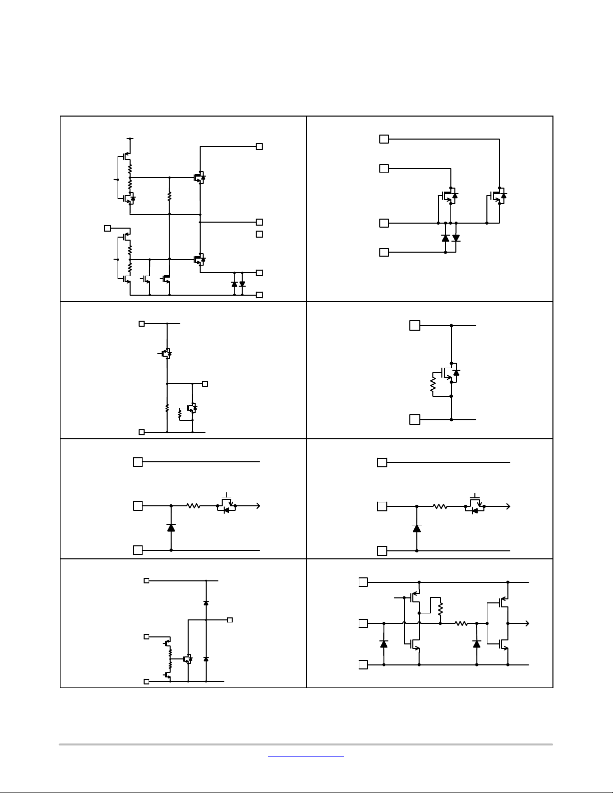
Simplified Equivalent Circuits
Table 8. PIN EQUIVALENT CIRCUIT
OUT1, OUT2
PVCC, VCC/SGND
(OUT +4.5 V)
PVCC
REG
VDD
VCC
IN1
IN2
VDD
FG
PWM
VCC
Table 6 shows the pin information. The pull−up/down
resistor and diode path are included.
PVCC
LV8314C
VCC
VDD
SGND
IN1
REG
OUT1
OUT2
RF
SGND
SGND
RF
VDD
SGND
VDD
IN2
SGND
VDD
SGND
FG
SGND
VDD
Low
200 kW
PWM
SGND
www.onsemi.com
9
Page 10
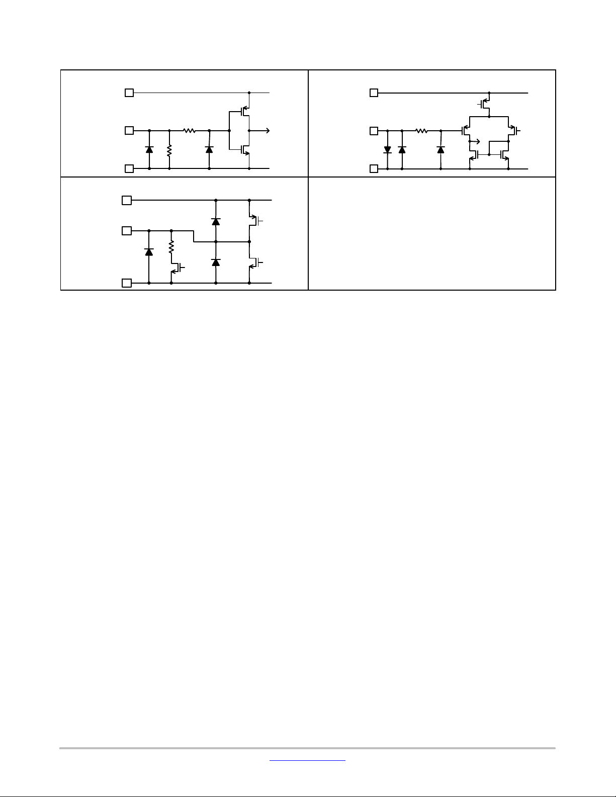
T
able 8. PIN EQUIVALENT CIRCUIT (continued)
TSL
RF
VDD
VDD
TSL2
VDD
LV8314C
TSL
SGND
TSL2
SGND
RF
200 kW
SGND
200 kW
High
www.onsemi.com
10
Page 11

LV8314C
Table 9. SOFT START END DUTY−CYCLE
SSTART_SEL
End Duty−cycle
0
24% output duty−cycle
1
54% output duty−cycle
Table 10. SOFT START DURATION TIME
INCTIM
Duration Time (s)
[1]
[0]
SSTART_SEL = 0
)
SSTART_SEL = 1
)
0
0
0.002
0.10
0
1
0.50
0.50
1
0
1.00
1.00
1
1
2.00
2.00
OPERATION DESCTIPTION
The LV8314C has various functions and parameters
which are defined by built−in registers. Refer to the Register
map and description page for the detail.
Spin−up Sequence
To spin−up a motor, power is applied to VCC pin and the
appropriate input PWM signal (see “DUTY_L” and
“DUTY_S” setting description in section “Steady rotation”)
is applied to PWM pin. The LV8314C starts driving the
motor whose current direction is determined by the Hall
sensor signal.
To avoid the unnecessary rush current, the “soft start”
mode is provided, which gradually increases output
duty−cycle. After the soft start mode, LV8314C goes to
steady rotation mode. The detail of the soft start mode and
steady rotation mode are described in the sections below.
If a motor already rotates at the power on in faster speed
than 304 rpm, the soft start mode is skipped and goes to
steady rotation mode immediately.
Soft Start
For soft start mode, the duty−cycle ramp up profile is
defined by the initial duty−cycle, slope, and exit condition.
The initial duty−cycle is fixed and it starts from 4%. The
slope is programmable. It is determined by registers
“SSTART_SEL” and “INCTIM”. The duty−cycle is
increased up to the end duty−cycle “SSTART_SEL” for
duration time “INCTIM”. The end duty−cycle is selectable
at 24% or 54% (see Table 9). The duration time can be
selected from 0.002 s to 2.0 s (see Table 10). The exit
condition means it’s in the state of either the duty−cycle
reaches “SSTART_SEL”. Soft start operation requires at
least 8 electrical cycles (4 mechanical cycles in case of 4
poles single phase motor) independent on the exit condition.
(End Duty−cycle = 24%
(End Duty−cycle = 54%
Figure 4 shows the image of soft start mode.
Figure 4. The Image of Soft Start Exit by End Duty−cycle
www.onsemi.com
11
Page 12

LV8314C
As the blue curve shown in Figure 4, the output
duty−cycle in the soft start mode starts from 4% of the output
duty. Then the output duty−cycle is increased to the end
duty−cycle linearly, which is shown by yellow circle. After
that, LV8314C goes to the steady rotation mode.
Figure 5 is the example of the duration time in case of
“SSTART_SEL = 1”.
Figure 5. Example: The Image of Soft Start
Duration Time in Case of SSTART_SEL = 1
Steady Rotation
The motor speed is defined by the output duty−cycle
which is controlled by input PWM pin.
The input PWM frequency range is 7 kHz − 40 kHz. The
output frequency is fixed to 48 kHz and it is not related to
input PWM frequency. Figure 6 shows the output
duty−cycle control profile which is relationship between
input PWM duty−cycle and the target output duty−cycle.
Registers to determine this relationship are;
TAG_L (Address 0x0100 D [7:1]): Minimum output
duty−cycle
TAG_H (Address 0x0101 D [7:1]): Maximum output
duty−cycle
DUTY_L (Address 0x0102 D [6:1]): Minimum input
duty−cycle
DUTY_H (Address 0x0103 D [6:1]): Maximum input
duty−cycle
FULL (Address 0x0108 D [2]): Output duty−cycle selection
at input duty−cycle over DUTY_H
DUTY_S (Address 0x0108 D [3]): Output duty−cycle
selection at input duty−cycle under DUTY_L
The detail of each register will be explained later.
Figure 6. Target Output Duty−cycle Control Profile
TAG_L/TAG_H: Minimum/Maximum Target Output
Duty−cycle Setting
The minimum output duty−cycle is set by “TAG_L” and
the maximum output duty−cycle is set by “TAG_H” within
the range of DUTY_L and DUTY_H. (See Figure 7.)
Figure 7. Max/Min Speed Setting
Do not set the maximum output duty−cycle setting
(TAG_H) less than the minimum output duty−cycle setting
(TAG_L).
www.onsemi.com
12
Page 13

LV8314C
DUTY_L/DUTY_H: Minimum/Maximum Input Duty−cycle
Setting
The range of PWM input duty−cycle can be set by the
registers “DUTY_L” and “DUTY_H” whose range is 0 to
100%. The equation of resolution is;
DUTY_L
D
+
min
max
DUTY_H
+
D
Where D
D
Do not set “DUTY_H” less than “DUTY_L”.
Figure 8 shows the relationship between input duty−cycle
and target output duty−cycle. TAG_L/TAG_H define the
start and end points of the output duty−cycle curve and the
value between (DUTY_L, TAG_L) and (DUTY_H,
TAG_H) are interpolated linearly.
49.8 [%]
63
49.8 ) 50.2 [%]
63
is minimum input duty−cycle
min
is maximum input duty−cycle
max
(eq. 2)
(eq. 3)
Figure 9. Max Speed Function Setting
DUTY_S: Speed Selection at Input Duty−cycle under
DUTY_L
For the behavior at input duty−cycle which is under
DUTY_L, the register “DUTY_S” provides two options.
DUTY_S = 0 i s t o keep the speed specified by “TAG_L” and
DUTY_S = 1 is to go to 0% output duty−cycle as shown in
Figure 10.
Figure 8. Input Duty−cycle Setting
FULL: Speed Selection at Input Duty−cycle over
DUTY_H
For the behavior at input duty−cycle which is over
DUTY_H, the register “FULL” provides two options.
FULL = 0 is to keep the speed specified by “TAG_H” and
FULL = 1 is to go to 100% output duty−cycle−cycle as
shown in Figure 9.
www.onsemi.com
Figure 10. Min Speed Function Setting
13
Page 14
LV8314C
Table 11. RATE OF CHANGE FOR OUTPUT DUTY
PWM_ROC
Rate of Change for Output Duty [%]
0
0.2% per 128 pulses
1
0.2% per 256 pulses
2
0.2% per 512 pulses
3
Change immediately to the target
Output Duty−cycle Transitions
When PWM i nput duty cycle changes, output PWM tar get
duty changes along with input and output characteristics
setting. The rate that actual output duty−cycle changes is set
by the register “PWM_ROC”. Actual output duty−cycle
transfers gradually to the target according to the rate which
is defined by PWM_ROC as shown in Table 11. In addition,
this register setting is effective not only in changing the input
duty−cycle but also in changing the mode from Start−up to
normal.
Output Waveform
The output pulse signal is about 0 V − VCC. The duty
before commutation change decreases gradually to 0% and
the duty after commutation change increases gradually to
the duty level controlled by speed control function by
built−in function called soft−switch. This state is shown in
Figure 11 as a schematic view.
Figure 11. Output Waveform Image
Soft−Switch Setting
Figure 12 shows the soft switch image. Due to the
soft−switch, the averaged output voltage can has the slope.
Rise
Rise Fall
Figure 12. L (Length) and S (Soft−Switch) Image
Fall
www.onsemi.com
14
Page 15

LV8314C
Table 12. SOFT−SWITCH PERIOD ADJUSTMENT
SSWHIGH_F
S/L Ratio
SSWHIGH_F
S/L Ratio
0
2.9%
8
26.4%
1
5.9%
9
29.3%
2
8.8%
10
32.2%
3
11.7%
11
35.2%
4
14.6%
12
38.1%
5
17.6%
13
41.0%
6
20.5%
14
43.9%
7
23.4%
15
46.9%
The soft switch period in beginning of commutation is
called “Rise soft−switch” and in end of commutation is
called “Fall soft−switch”. The LV8314C can adjust both soft
switch periods independently as the ratio of L and S shown
in Figure 12. “SSWHIGH_F” and “SSWLOW_F” define
the period of “Rise soft−switch” and “SSWHIGH” and
“SSWLOW” define the period of “Fall soft−switch”. These
soft switch periods are defined by equation 4.
Soft switch period [%] +
S
100
L
(eq. 4)
Where:
S is soft−switch period
L is one commutation period
SSWHIGH_F and SSWHIGH are for the maximum
output duty−cycle defined by TAG_H and SSWLOW_F and
SSWLOW are for the minimum output duty−cycle defined
by TAG_L. All register have 4bits and Table 12 shows the
adjustable values.
SSWLOW_F
SSWHIGH
SSWLOW
SSWLOW_F
SSWHIGH
SSWLOW
Once these registers are set, the ratio of soft−switch in
other speed settings is as shown in Figure 13.
SSWLOW_F or SSWLOW setting value
SSWHIGH_F = SSWLOW_F or
SSWHIGH = SSWLOW
SSWHIGH_F or SSWHIGH setting value
Figure 13. The Relationship between Soft−Switch
and Speed
FG Output
FG signal output is decided by the Hall signal cross point.
The relationship between motor speed and FG frequency in
the state “T ACHSEL = 0” represents the following equation.
p
fFG[Hz] +
60
N
2
(eq. 5)
Where N: Motor speed [rpm] and p: Number of Pole
Figure 14 shows the timing chart of the hall sensor output
and the FG output.
Figure 14. Timing Chart of Output
www.onsemi.com
15
Page 16

Output signal in FG pin can be selected by setting the
Table 13. TYPE OF OUTPUT SIGNAL IN FG PIN
TACHSEL
Output Signal in FG Pin
0
FG signal as shown in Figure 14
1
2 times frequency of FG signal
2
one half the frequency of FG signal
3
RD signal (The polarity is decided by RD_INV
register “TACHSEL” as shown in Table 13 and Figure 15.
register)
Figure 15. FG Signal vs. TACHSEL Setting
LV8314C
When TACHSEL is set to 1 or 2, FG signal starts from
LOW in POR regardless of rotor position as shown in
Figure 16. Note that in some cases FG signal cannot keep the
Figure 16. FG State by TACHSEL Setting
50% duty−cycle when the rotation restarts from the stop or
the rotation speed changes suddenly as shown in Figure 17.
IN1<IN2: FG=H
Figure 17. FG Duty−cycle
www.onsemi.com
16
Page 17

LV8314C
Table 14. LEAD−ANGLE ADJUSTMENT
DL_RESO
Lead−Angle
Range of
0
0.70
0−10.5
1
0.35
0−5.25
Lead−Angle Setting
In the output, the output current delays from the output
voltage because of the inductance of motor coil. The output
current which flows in a motor coil generates torque for the
motor and the torque is maximized by the synchronization
of output current with the BEMF phase. Therefore, this
delay decreases an efficiency of motor rotation. It is
generally increased in proportion to the rotational speed.
The LV8314C can cancel the delay by earlier
commutation than the Hall sensor signal as shown in
Figure 18. This phase adjustment is called the “lead−angle”.
In Figure 18, when the output voltage VOUT1 and the
output current IOUT1 in black are changed to the waveform
in red after the lead−angle adjustment and it is the most
optimum commutation timing.
Figure 18. The Relationship between the Lead−Angle and the Delay of Output Current
The relationship between output duty−cycle and
lead−angle is shown in Figure 19. The optimum lead−angle
will vary by the motor characteristics so it is necessary to
adjust the lead−angle based on the motor in use.
Figure 19. Lead−angle Curve Image
The LV8314C can set the lead−angle at maximum target
output duty−cycle (TAG_H) and at minimum target output
duty−cycle (TAG_L) by “DLDEG_H” and “DLDEG_L”
individually. These parameters have 4 bits. The direction of
lead−angle is defined by the MSB bit of “DLDEG_H” and
“DLDEG_L”. When they are set to “0”, the direction of
lead−angle is the behind, it means the output voltage
commutation is slower than the Hall sensor signal. When
they are set to “1”, the direction is the advance, it means the
output voltage commutation is earlier than the Hall sensor
signal, that is, the output voltage commutation is earlier than
the Hall sensor signal. The adjustable range and the
resolution are determined by “DL_RESO” setting as shown
in Table 14.
Resolution
°
°
Lead−Angle
°
°
The lead−angles are expressed in the following equations.
L
+ Res DLDEGH[deg]
max
L
+ Res DLDEGL[deg]
min
(eq. 6)
(eq. 7)
where:
Lmax: lead−angle at maximum target output duty−cycle
(TAG_H)
www.onsemi.com
17
Page 18

LV8314C
Table 15. UVLO TRUTH TABLE
Input
Output
IN1
IN2
OUT1
OUT2
LHL
Hi−Z
HLHi−Z
L
Table 16. RD SIGNAL
Normal Rotation
Lock Rotation
RD_INV = 0
Low
High
RD_INV = 1
High
Low
Lmin: lead−angle at minimum target output duty−cycle
(TAG_L)
Res: The resolution of lead−angle defined by “DL_RESO”
Once DLDEG_H and DLDEG_L are set, the lead−angle
in other output duty−cycle is set to interpolated and
extrapolated value according to the output duty−cycle, even
though the output duty−cycle is defined by FULL = 1.
Protections
The LV8314C has the following protection functions.
• TSD (Thermal Shut Down)
• UVLO (Under Voltage Lock Out)
• Lock protection
• CLM (Current Limiter)
• OCP (Over Current Protection)
When the TSD, OCP or Lock protection works, all of the
internal FETs are turned off. When UVLO or CLM works,
the output PWM is off and the motor goes to re−circulation
mode with asynchronous operation.
Thermal Shutdown Protection (TSD)
When LV8314C junction temperature rises to 180°C,
TSD will activate and turns off high−side and low−side
Power FET. Therefore, OUT1 and OUT2 will become high
impedance and the coil current will shut off. When it falls
under 140°C, TSD will is deactivated and motor will start to
rotate.
Under Voltage Lock Out (UVLO)
When VCC voltage goes to low level (3.4 V(typ)), UVLO
will active and stop the motor. VCC voltage is recovered to
above detection voltage (3.4 V(typ)) plus hysteresis voltage
(0.2 V(typ)).
The TRUTH TABLE of Operating State with UVLO is as
shown in Table 15.
Lock Detection and Lock Protection
When the motor is locked, the heat is continuously
generated because the LV8314C keeps trying to rotate the
motor.
The lock protection works to prevent such a heat
generation by turning OUT1 and OUT2 into high impedance
and shutting off the motor current. When a motor is locked
in the steady rotation mode and the L V8314C doesn’t detect
the FG edge for more than 0.3 s which is equivalent to
50 rpm, the lock protection works (Figure 20).
The lock protection signal can be output from FG pin by
setting the register “TACHSEL”. In this mode, the RD signal
goes to “High”, though it is “Low” at motor starts when
“RD_INV” is sets to 0. Table 16 shows the behavior of RD
signal.
When the motor restarts and IC detects 4 phase changes
at least (depends on rotation speed), the RD signal goes to
“Low”.
Figure 20. Timing Chart of the Lock Protection
www.onsemi.com
18
Page 19

LV8314C
Table 17. STAND−BY PERIOD FOR FG
LOCK_DET
Stand−by Period for FG [s]
0
0.7
1
1.0
Figure 21. The Relationship between Protection Time and the Number of Protection Times
Figure 21 shows the relationship between protection
period and the number of protection times. The 1st to 4th
protection period take 3.5 s and 5th and subsequent
protection period takes 14 s.
After the period of motor lock protection, the LV8314C
tries to rotate the motor and stand−by for FG edge for a
certain period defined by “LOCK_DET” as shown in
Table17.
To reset the lock protection mode, low duty−cycle to set
output PWM duty below 5% must be applied to the PWM
input signal. T o retry the motor rotation, proper duty−cycle
must be applied to the PWM input signal.
These protection periods and the number of protection
times are applied in accordance with the internal counter. If
the duty−cycle to set output PWM duty below 5% is input
during lock protection period, the lock protection counter
will keep to count the protection period and the protection
state is not changed. Figure 22 shows this counter behavior.
www.onsemi.com
19
Page 20

LV8314C
Figure 22. Lock Protection Counter Continues During Lock Protection Period
The lock protection period is changed by the condition of
output signal. If the duty−cycle to set output PWM duty
below 5% is input and the output signals are disappeared
during the restart period in lock protection period, the
www.onsemi.com
counter is reset and the lock protection counter will activate
from the initial state starting from PWM Pos−Edge and the
protection period will start from 1
st
time as shown in
Figure 23 and Figure 24.
20
Page 21
LV8314C
Table 18. CLM THRESHOLD LEVEL
CL_LVL
CLM Threshold Level
0
100 mV
1
75 mV
Table 19. CLM MASK TIME
OCP_MASK
CLM Mask Time [ms]
0
0.511.0
Figure 23. Lock Protection Counter Reset During Motor Restart after 3.5 s Lock Protection Period
Figure 24. Lock Protection Counter Reset During Motor Restart after 14 s Lock Protection Period
Current Limiter (CLM)
When the coil current becomes large, CLM will activate
and then output will be in the re−circulation state. The
current is monitored by RF pin and the threshold can be
selectable by “CL_LVL” as shown in Table 18.
While CLM is active, synchronous rectification of the
output becomes disabled. “OCP_MASK” sets the masking
time to ignore upper and lower FET’s reverse recovery.
Table 19 shows the mask time.
www.onsemi.com
21
Page 22

LV8314C
Overcurrent Protection (OCP)
OCP monitors the coil current by RF pin and if it becomes
larger than 150 mV even if CLM is activated, OCP works to
prevent the device or motor from breakdown. OCP
operation is to turn OUT1 and OUT2 into high impedance
and to shut off the motor current.
This function has also the mask time same as CLM
function shown in Table 19.
Register called “OCP_LAT_CLR” allows to select
behavior when OCP is activated. One is to keep the motor
stopped until the next power on sequence, and the other one
is to activate Lock protection mode.
Nonvolatile Memory
The L V8314C has internal nonvolatile memory which can
store register values which define various parameters and
settings. The stored register values will be reloaded at POR
shown as Figure 25.
The LV8314C Evaluation kit can support NVM
programming. For the detail, please see the EVK user guide
“EVBUM2735−D”.
Figure 25. Image of the Internal Register and Nonvolatile Memory
SPI Communication
The LV8314C allows SPI communication. Through
provided the Evaluation kit, various parameter registers can
be accessed. For the detail, please see EVK user guide
“EVBUM2735−D”.
www.onsemi.com
22
Page 23

REGISTER MAP
Table 20. GENERIC STRADDLE TABLE
Register
D7D6D5D4D3D2D1
D0
0x0000
0xAA10101010
0x0001
0x5501010101
0x0002
0x0000
RECALC_
RELOAD_
0x0003
0x00
RELOAD
0x0004
0x00
RECALC
0x0005
0x18
Identification Number
0x0100
0x00
TAG_L[7:1]
0
0x0101
0xFE
TAG_H[7:1]
0
0x0102
0x00
0
DUTY_L[6:1]
0
0x0103
0xFF
1
DUTY_H[6:1]
1
0x0104
0x90
DLDEG_H[4:1]
DLDEG_L[4:1]
0x0105
0x8F
SSWHIGH_F[3:0]
SSWLOW_F[3:0]
0x0106
0x8F
SSWHIGH[3:0]
SSWLOW[3:0]
0x0107
0x56
PWM_ROC[1:0]
TACHSEL[1:0]
RD_INV
SSTART_
INCTIM[1:0]
0x0108
0xA5
DLDEG_
DLDEG_
DL_RESO
PWMIN_
DUTY_S
FULL
CL_LVL
DRV
0x0109
0x20
PWMAV[1]
PWMAV[0]
LOCK_EN
LOCK_
OCP_
OCP_
0x010A
0x000000
0
0x010B
0x00
Reserved
0
0x010C
0x00
ON_INTERNAL
0x010D
0x0000
Register Map
Internal register map can be classified into four types as
shown in Table 20.
Read Only
Read/Write, User defined registers to be written to nonvolatile memory
Read/Write
Write only (Auto clear)
Address Initial
LV8314C
H[0]
L[0]
INV
SEL
DET
EN
LAT_CLR
(0)
EN
MODE
MASK
Registers in the black cells do not exist. Therefore, these
registers cannot be written and the read values are always
zero. The bits with numeric values (0 or 1) must remain
as−is.
There are some register addresses which contain both the
bits stored in NVM and the bits not stored in NVM. Confirm
the bit types to save the data to NVM.
www.onsemi.com
23
Page 24
Register Description
T able 21. REGISTER ADDRESS 0x0000−0x0005 Register Description 1
Function
Address
Bits
Register Name
Description
Fixed register 1
0x0000
[7:0]
−
Data of 0xAA are stored. (Read only)
Fixed register 2
0x0001
[7:0]
−
Data of 0x55 are stored. (Read only)
Enable re−calculation
0x0002
[1]
RECALC_EN
This register enable re−calculation of Speed/
Register re−loading
0x0002
[0]
RELOAD_EN
This register enables data reloading from NVM.
Register re−loading
0x0003
RELOAD
When this bit is set to 1, data reloading from NVM
Trigger of re−calculation
0x0004
[0]
RECALC
When this bit is set to 1, re−calculation of Speed/
Device ID
0x0005
[7:0]
ID_NUMBER
Data of device ID are stored. (Read only)
Table 22. REGISTER ADDRESS 0x0100−0x0109 Register Description 2
Function
Address
Bits
Register Name
Description
Minimum speed setting
0x0100
[7:1]
TAG_L
s.
Maximum speed setting
0x0101
[7:1]
TAG_H
Minimum input duty cycle
0x0102
[6:1]
DUTY_L
These registers set minimum input duty−cycle.
Maximum input duty cycle
0x0103
[6:1]
DUTY_H
These registers set maximum input duty−cycle.
Lead−angle setting at
0x0104
[3:0]
DLDEG_L
This register adjusts lead−angle at rotational
Lead−angle setting at
0x0104
[7:4]
DLDEG_H
This register adjusts lead−angle at rotational
LV8314C
Lead Angle/Soft SW setting.
0: Disable
1: Enable
(memory to register)
(memory to register)
setting
setting
[0]
0: Disable
1: Enable
is executed while RELOAD_EN is set to 1.
This register is auto clear type.
Lead Angle/Soft SW setting is executed while
RECALC_EN is set to 1.
This register is auto clear type.
These registers set minimum/maximum output
duty−cycle.
000 0000: 0%
111 1111: 100%
Also 111 1110 and 111 1111: 100%
*Refer to the section “Steady Rotation” for detail
00 0000: Duty 0%
11 1111: Duty 49.3%
00 0000: Duty 50.4%
11 1111: Duty 100%
minimum speed
maximum speed
0x0108
0x0108
[6]
[7]
www.onsemi.com
speed set by TAG_L.
0000: 0°,
1111: −5.25 or −10.5°
(DLDEG_L[4] = 0)
0000: 0°,
1111: +5.25 or +10.5°
(DLDEG_L[4] = 1)
*Refer to register of “DL_RESO” description.
speed by TAG_H.
0000: 0°,
1111: −5.25 or −10.5°
(DLDEG_H[4] = 0)
0000: 0°,
1111: +5.25 or +10.5°
(DLDEG_H[4] = 1)
*Refer to register of “DL_RESO” description.
24
Page 25

LV8314C
T
Soft switch width setting at
0x0105
[7:4]
SSWHIGH_F
Soft switch width of top is set at rotational speed
Soft switch width setting at
0x0105
[3:0]
SSWLOW_F
Soft switch width of top is set at rotational speed
Soft switch width setting at
0x0106
[7:4]
SSWHIGH
Soft switch width of tail is set at rotational speed
Soft switch width setting at
0x0106
[3:0]
SSWLOW
Soft switch width of tail is set at rotational speed
Increment Ratio of the Output
0x0107
[7:6]
PWM_ROC
This register sets the increment ratio of the
FG/RD select
0x0107
[5:4]
TACHSEL
This register sets FG pin function.
RD polarity select
0x0107
[3]
RD_INV
RD polarity select at RD output by TACHSEL
Soft start end duty−cycle
0x0107
[2]
SSTART_SEL
This register sets Soft start end duty−cycle.
Soft start release time
0x0107
[1:0]
INCTIM
This register sets the soft start duration time.
Lead angle resolution select
0x0108
[5]
DL_RESO
This register sets the lead angle resolution and
Speed control slope invert
0x0108
[4]
PWMIN_INV
Control slope polarity for input duty−cycle is
able 22. REGISTER ADDRESS 0x0100−0x0109 Register Description 2 (continued)
Function DescriptionRegister NameBitsAddress
maximum speed
minimum speed
maximum speed
minimum speed
duty−cycle
set by TAG_H.
0000: 2.9% equivalency of one commutation
period.
1111: 46.9% equivalency of one commutation
period.
set by TAG_L.
0000: 2.9% equivalency of one commutation
period.
1111: 46.9% equivalency of one commutation
period.
set by TAG_H.
0000: 2.9% equivalency of one commutation
period.
1111: 46.9% equivalency of one commutation
period.
set by TAG_L.
0000: 2.9% equivalency of one commutation
period.
1111: 46.9% equivalency of one commutation
period.
output−duty.
00: 0.2% per 128 pulses
01: 0.2% per 256 pulses
10: 0.2% per 512 pulses
11: Change immediately to target output
duty−cycle
00: FG output (1 times hall frequency)
01: FG output (2 times hall frequency)
10: FG output (0.5 times hall frequency
11: RD output (Polarity is decided by RD_INV
register)
register.
0: Low in rotation, High in lock protection
1: High in rotation, Low in lock protection
0: 24% output duty−cycle
1: 54% output duty−cycle
*Refer to the section “Soft Start” for details.
width.
0: 0.70° per DLDEG register, adjustment
width is ±10.5°
1: 0.35° per DLDEG register, adjustment
width is ±5.25°
changed.
0: Normal mode (Low duty−cycle is low speed
rotation)
1: Invert mode (Low duty−cycle is high speed
rotation)
www.onsemi.com
25
Page 26

LV8314C
T
Minimum speed setting 2
0x0108
[3]
DUTY_S
This register sets the speed when input
Maximum speed setting 2
0x0108
[2]
FULL
This register defines the output behavior when
CLM threshold level select
0x0108
[1]
CL_LVL
This register sets current limiter threshold level.
Sync/Async drive select
0x0108
[0]
DRVMODE
This register selects synchronous/asynchronous
Input PWM average setting
0x0109
[5:4]
PWMAV
The number of times to perform averaging for
Lock protection enable
0x0109
[3]
LOCK_EN
This register selects enable or disable of the lock
r
Standby period for FG pulse
0x0109
[2]
LOCK_DET
This register sets standby period for FG pulse in
Condition to enter Lock
0x0109
[1]
OCP_LAT_CLR
This register selects the status when OCP is
Mask time for reverse
0x0109
[0]
OCP_MASK
This register sets the masking time to ignore the
e
ORDERING INFORMATION
Device Order Number
Specific Device Marking
Package Type
Shipping
†
LV8314CGR2G
LV8314C
TSSOP−14
2500 / Tape & Reel
able 22. REGISTER ADDRESS 0x0100−0x0109 Register Description 2 (continued)
Function DescriptionRegister NameBitsAddress
duty−cycle is less than DUTY_L.
0: Fixed speed set by DUTY_L
1: Fixed output duty−cycle of 0%
input PWM is greater than the duty cycle set by
DUTY_H.
0: Fixed speed set by TAG_H
1: Fixed duty cycle of 100% with soft switch
0: 100 mV
1: 75 mV
drive.
0: High−side switching is PWM. Low−side
switching is asynchronous
1: High−side switching is PWM. Low−side
switching is synchronous
input PWM duty cycle.
00: Averaged 4 times
01: Averaged 8 times
10, 11: Not averaged
protection function.
0: Lock protection disable
1: Lock protection enable
Please set it to 0 for normal use. To set to 1 is fo
test use only.
in Lock protection
Protection mode in OCP
active
recovery time setting
†For information on tape and reel specifications, including part orientation and tape sizes, please refer to our Tape and Reel Packaging
Specifications Brochure, BRD8011/D.
Lock protection.
0: 0.7 s
1: 1.0 s
activated.
0: The motor stops until next power on
sequence
1: The IC goes to “Lock Protection mode”
reverse recovery for both high−side and low−sid
Power FET.
0: 0.5 ms
1: 1.0 ms
(Pb−Free)
www.onsemi.com
26
Page 27

TSSOP−14 WB
0.10 (0.004)
P
−T−
SEATING
PLANE
LV8314C
PACKAGE DIMENSIONS
CASE 948G
ISSUE C
14X REFK
S
U
T
S
N
0.25 (0.010)
U0.15 (0.006) T
S
2X L/2
0.10 (0.004) V
14
M
8
M
L
PIN 1
IDENT.
1
S
U0.15 (0.006) T
A
−V−
B
N
−U−
F
7
DETAIL E
K
K1
J
J1
SECTION N−N
C
D
G
H
DETAIL E
SOLDERING FOOTPRINT
NOTES:
1. DIMENSIONING AND TOLERANCING PER
ANSI Y14.5M, 1982.
2. CONTROLLING DIMENSION: MILLIMETER.
3. DIMENSION A DOES NOT INCLUDE MOLD
FLASH, PROTRUSIONS OR GATE BURRS.
MOLD FLASH OR GATE BURRS SHALL NOT
EXCEED 0.15 (0.006) PER SIDE.
4. DIMENSION B DOES NOT INCLUDE
INTERLEAD FLASH OR PROTRUSION.
INTERLEAD FLASH OR PROTRUSION SHALL
NOT EXCEED 0.25 (0.010) PER SIDE.
5. DIMENSION K DOES NOT INCLUDE DAMBAR
PROTRUSION. ALLOWABLE DAMBAR
PROTRUSION SHALL BE 0.08 (0.003) TOTAL
IN EXCESS OF THE K DIMENSION AT
MAXIMUM MATERIAL CONDITION.
6. TERMINAL NUMBERS ARE SHOWN FOR
REFERENCE ONLY.
7. DIMENSION A AND B ARE TO BE
DETERMINED AT DATUM PLANE −W−.
INCHESMILLIMETERS
−W−
DIM MIN MAX MIN MAX
A 4.90 5.10 0.193 0.200
B 4.30 4.50 0.169 0.177
C −−− 1.20 −−− 0.047
D 0.05 0.15 0.002 0.006
F 0.50 0.75 0.020 0.030
G 0.65 BSC 0.026 BSC
H 0.50 0.60 0.020 0.024
J 0.09 0.20 0.004 0.008
J1 0.09 0.16 0.004 0.006
K 0.19 0.30 0.007 0.012
K1 0.19 0.25 0.007 0.010
L 6.40 BSC 0.252 BSC
M 0 8 0 8
____
7.06
1
0.65
PITCH
14X
0.36
ON Semiconductor and are trademarks of Semiconductor Components Industries, LLC dba ON Semiconductor or its subsidiaries in the United States and/or other countries.
ON Semiconductor owns the rights to a number of patents, trademarks, copyrights, trade secrets, and other intellectual property. A listing of ON Semiconductor ’s product/patent
coverage may be accessed at www.onsemi.com/site/pdf/Patent−Marking.pdf. ON Semiconductor reserves the right to make changes without further notice to any products herein.
ON Semiconductor makes no warranty, representation or guarantee regarding the suitability of its products for any particular purpose, nor does ON Semiconductor assume any liability
arising out of the application or use of any product or circuit, and specifically disclaims any and all liability, including without limitation special, consequential or incidental damages.
Buyer is responsible for its products and applications using ON Semiconductor products, including compliance with all laws, regulations and safety requirements or standards,
regardless of any support or applications information provided by ON Semiconductor. “Typical” parameters which may be provided in ON Semiconductor data sheets and/or
specifications can and do vary in different applications and actual performance may vary over time. All operating parameters, including “Typicals” must be validated for each customer
application by customer’s technical experts. ON Semiconductor does not convey any license under its patent rights nor the rights of others. ON Semiconductor products are not
designed, intended, or authorized for use as a critical component in life support systems or any FDA Class 3 medical devices or medical devices with a same or similar classification
in a foreign jurisdiction or any devices intended for implantation in the human body. Should Buyer purchase or use ON Semiconductor products for any such unintended or unauthorized
application, Buyer shall indemnify and hold ON Semiconductor and its officers, employees, subsidiaries, affiliates, and distributors harmless against all claims, costs, damages, and
expenses, and reasonable attorney fees arising out of, directly or indirectly, any claim of personal injury or death associated with such unintended or unauthorized use, even if such
claim alleges that ON Semiconductor was negligent regarding the design or manufacture of the part. ON Semiconductor is an Equal Opportunity/Affirmative Action Employer. This
literature is subject to all applicable copyright laws and is not for resale in any manner.
14X
1.26
DIMENSIONS: MILLIMETERS
UBLICATION ORDERING INFORMATION
LITERATURE FULFILLMENT:
Email Requests to: orderlit@onsemi.com
ON Semiconductor Website: www.onsemi.com
TECHNICAL SUPPORT
North American Technical Support:
Voice Mail: 1 800−282−9855 Toll Free USA/Canada
Phone: 011 421 33 790 2910
◊
www.onsemi.com
Europe, Middle East and Africa Technical Support:
Phone: 00421 33 790 2910
For additional information, please contact your local Sales Representative
27
 Loading...