

Page 1
Single, Dual, Quad
Low-Voltage, Rail-to-Rail
Operational Amplifiers
LMV321, NCV321, LMV358,
LMV324
The LMV321, LMV321I, NCV321, LMV358/LMV358I and
LMV324 are CMOS single, dual, and quad low voltage operational
amplifiers with rail−to−rail output swing. These amplifiers are a
cost−effective solution for applications where low power consumption
and space saving packages are critical. Specification tables are
provided for operation from power supply voltages at 2.7 V and 5 V.
Rail−to−Rail operation provides improved signal−to−noise
preformance. Ultra low quiescent current makes this series of
amplifiers ideal for portable, battery operated equipment. The
common mode input range includes ground making the device useful
for low−side current−shunt measurements. The ultra small packages
allow for placement on the PCB in close proximity to the signal source
thereby reducing noise pickup.
Features
• Operation from 2.7 V to 5.0 V Single−Sided Power Supply
• LMV321 Single Available in Ultra Small 5 Pin SC70 Package
• No Output Crossover Distortion
• Rail−to−Rail Output
• Low Quiescent Current: LMV358 Dual − 220 mA, Max per Channel
• No Output Phase−Reversal from Overdriven Input
• NCV Prefix for Automotive and Other Applications Requiring
Unique Site and Control Change Requirements; AEC−Q100
Qualified and PPAP Capable
• These Devices are Pb−Free, Halogen Free/BFR Free and are RoHS
Compliant
www.onsemi.com
1
SC−70
CASE 419A
1
Micro8
CASE 846A
8
1
SOIC−8
CASE 751
1
SOIC−14
CASE 751A
ORDERING AND MARKING INFORMATION
See detailed ordering and shipping information in the package
dimensions section on page 12 of this data sheet.
5
1
TSOP−5
CASE 483
8
1
UDFN8
CASE 517AJ
1
TSSOP−14
CASE 948G
Typical Applications
• Notebook Computers and PDA’s
• Portable Battery−Operated Instruments
• Active Filters
© Semiconductor Components Industries, LLC, 2015
January, 2021 − Rev. 16
1 Publication Order Number:
LMV321/D
Page 2
LMV321, NCV321, LMV358, LMV324
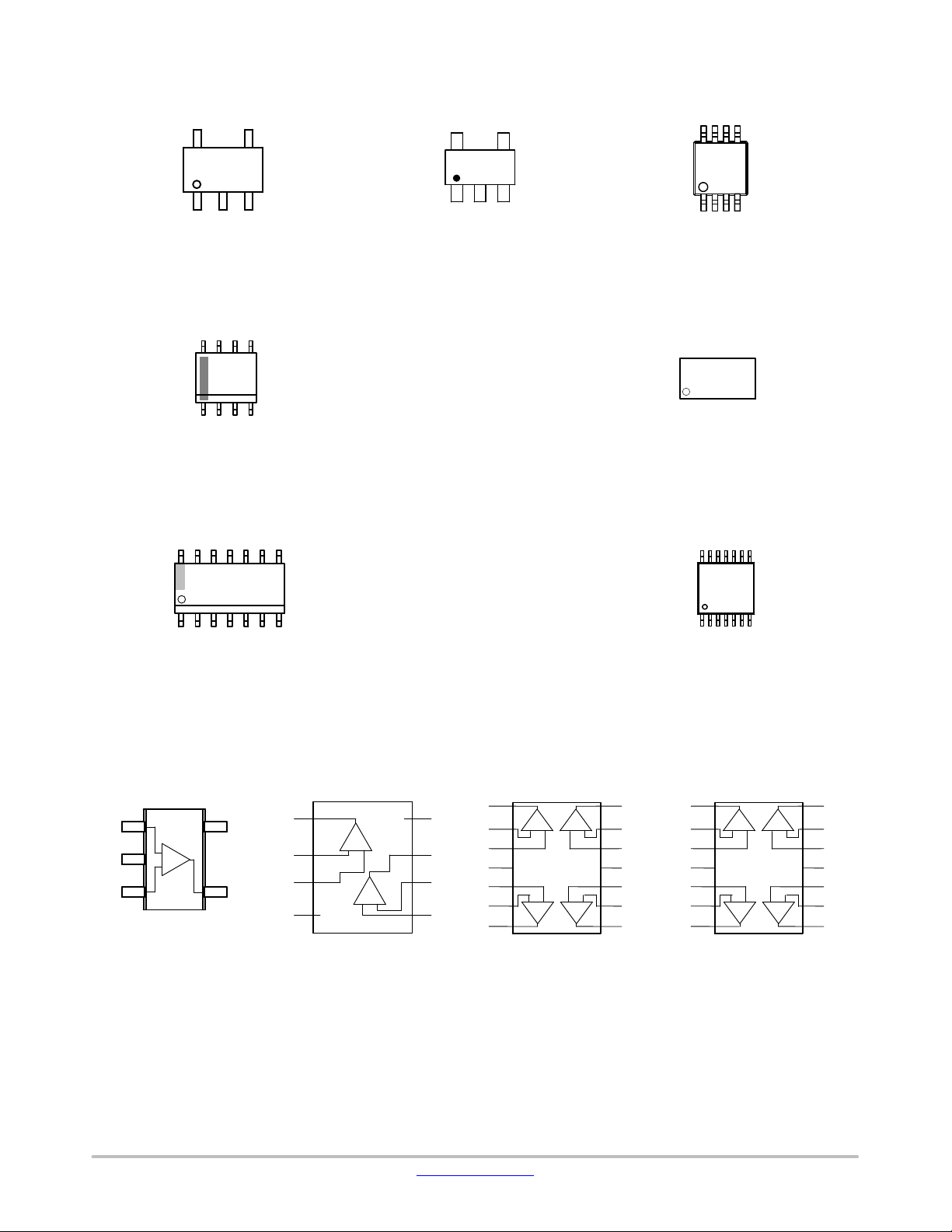
SC−70
AAC MG
G
AAC = Specific Device Code
M = Date Code
G = Pb−Free Package
(Note: Microdot may be in either location)
SOIC−8
8
V358
ALYW
G
1
V358 = Specific Device Code
A = Assembly Location
L = Wafer Lot
Y = Year
W = Work Week
G = Pb−Free Package
SOIC−14 TSSOP−14
14
LMV324
AWLYWWG
1
LMV324 = Specific Device Code
A = Assembly Location
WL = Wafer Lot
Y = Year
WW = Work Week
G = Pb−Free Package
MARKING DIAGRAMS
TSOP−5
5
3ACAYWG
G
1
3AC = Specific Device Code
A = Assembly Location
Y = Year
W = Work Week
G = Pb−Free Package
(Note: Microdot may be in either location)
Micro8
8
V358
AYW G
G
1
V358 = Specific Device Code
A = Assembly Location
Y = Year
W = Work Week
G = Pb−Free Package
(Note: Microdot may be in either location)
UDFN8
AC M
G
AC = Specific Device Code
M = Date Code
G = Pb−Free Package
14
LMV
324
ALYW
1
LMV324 = Specific Device Code
A = Assembly Location
L = Wafer Lot
Y = Year
W = Work Week
G = Pb−Free Package
SC70−5/TSOP−5
1
+IN
2
−
V
3
−IN
(Top View)
PIN CONNECTIONS
UDFN8/Micro8/SOIC−8
+
V
OUTPUT
OUT A
IN A−
IN A+
1
A
− +
2
3
V−
4
+ −
B
5
+
−
4
8
7
6
5
V+
OUT B
IN B−
IN B+
OUT A
IN A−
IN A+
V+
IN B+
IN B−
OUT B
(Top View) (Top View) (Top View)
1
2
3
4
5
6
7
SOIC−14
− +A+ −
+ −
B C
14
OUT D
OUT A
D
13
IN D−
12
IN D+
11
V−
10
IN C+
9
IN C−
− +
8
OUT C
IN A−
IN A+
V+
IN B+
IN B−
OUT B
TSSOP−14
1
2
− +A+ −
3
4
5
6
7
+ −
B C
14
OUT D
D
13
IN D−
12
IN D+
11
V−
10
IN C+
9
IN C−
− +
8
OUT C
www.onsemi.com
2
Page 3
LMV321, NCV321, LMV358, LMV324
MAXIMUM RATINGS
Symbol Rating Value Unit
V
S
V
IDR
V
ICR
Maximum Input Current 10 mA
t
So
T
J
T
A
q
JA
T
stg
V
ESD
Stresses exceeding those listed in the Maximum Ratings table may damage the device. If any of these limits are exceeded, device functionality should not be assumed, damage may occur and reliability may be affected.
1. Continuous short−circuit operation to ground at elevated ambient temperature can result in exceeding the maximum allowed junction
temperature of 150°C. Output currents in excess of 45 mA over long term may adversely affect reliability. Shorting output to either V+
or V− will adversely affect reliability.
2. NCV prefix is qualified for automotive usage.
3. Human Body Model, applicable std. MIL−STD−883, Method 3015.7
Machine Model, applicable std. JESD22−A115−A (ESD MM std. of JEDEC)
Field−Induced Charge−Device Model, applicable std. JESD22−C101−C (ESD FICDM std. of JEDEC).
Supply Voltage (Operating Range VS = 2.7 V to 5.5 V) 5.5 V
Input Differential Voltage $Supply Voltage V
Input Common Mode Voltage Range −0.5 to (V+) + 0.5 V
Output Short Circuit (Note 1) Continuous
Maximum Junction Temperature 150 °C
Operating Ambient Temperature Range
LMV321, LMV358, LMV324
LMV321I, LMV358I
NCV321 (Note 2)
Thermal Resistance:
−40 to 85
−40 to 125
−40 to 125
°C
°C
°C
°C/W
SC−70 280
Micro8 238
TSOP−5 333
UDFN8 (1.2 mm x 1.8 mm x 0.5 mm) 350
SOIC−8 212
SOIC−14 156
TSSOP−14 190
Storage Temperature −65 to 150 °C
Mounting Temperature (Infrared or Convection −20 sec) 260 °C
ESD Tolerance (Note 3)
LMV321, LMV321I, NCV321
Machine Model
Human Body Model
100
1000
LMV358/358I/324
Machine Model
Human Body Mode
100
2000
V
www.onsemi.com
3
Page 4

LMV321, NCV321, LMV358, LMV324
2.7 V DC ELECTRICAL CHARACTERISTICS (Unless otherwise specified, all limits are guaranteed for T
R
= 1 MW, V− = 0 V, VO = V+/2)
L
= 25°C, V+ = 2.7 V,
A
Parameter Symbol Condition Min Typ Max Unit
Input Offset Voltage V
Input Offset Voltage Average Drift ICV
Input Bias Current I
Input Offset Current I
IO
OS
B
IO
TA = T
TA = T
TA = T
TA = T
Low
Low
Low
Low
to T
(Note 4) 1.7 9 mV
High
to T
(Note 4) 5
High
to T
(Note 4) <1 nA
High
to T
(Note 4) <1 nA
High
mV/°C
Common Mode Rejection Ratio CMRR 0 V v VCM v 1.7 V 50 63 dB
Power Supply Rejection Ratio PSRR 2.7 V v V+ v 5 V,
V
= 1 V
O
Input Common−Mode Voltage Range V
Output Swing
Supply Current LMV321, NCV321
LMV358/LMV358I (Both Amplifiers)
CM
V
OH
V
OL
I
CC
For CMRR w 50 dB 0 to 1.7 −0.2 to 1.9 V
RL = 10 kW to 1.35 V
RL = 10 kW to 1.35 V (Note 5)
LMV324 (4 Amplifiers)
2.7 V AC ELECTRICAL CHARACTERISTICS (Unless otherwise specified, all limits are guaranteed for T
R
= 1 MW, V− = 0 V, VO = V+/2)
L
Parameter
Symbol Condition Min Typ Max Unit
50 60 dB
VCC − 100 VCC − 10 mV
60 180 mV
80
140
260
A
185
340
680
= 25°C, V+ = 2.7 V,
mA
Gain Bandwidth Product GBWP CL = 200 pF 1 MHz
Phase Margin
Gain Margin G
Input−Referred Voltage Noise e
Q
m
m
n
f = 50 kHz 50 nV/√Hz
60 °
10 dB
Product parametric performance is indicated in the Electrical Characteristics for the listed test conditions, unless otherwise noted. Product
performance may not be indicated by the Electrical Characteristics if operated under different conditions.
4. For LMV321, LMV358, LMV324: T
For LMV321I, LMV358I, NCV321: T
5. Guaranteed by design and/or characterization.
= −40°C to +85°C
A
= −40°C to +125°C.
A
www.onsemi.com
4
Page 5
LMV321, NCV321, LMV358, LMV324
5.0 V DC ELECTRICAL CHARACTERISTICS (Unless otherwise specified, all limits are guaranteed for T
R
= 1 MW, V− = 0 V, VO = V+/2)
L
= 25°C, V+ = 5.0 V,
A
Parameter Symbol Condition Min Typ Max Unit
Input Offset Voltage V
Input Offset Voltage Average Drift TCV
Input Bias Current (Note 7) I
Input Offset Current (Note 7) I
IO
B
IO
TA = T
TA = T
IO
TA = T
TA = T
Low
Low
Low
Low
to T
(Note 6) 1.7 9 mV
High
to T
(Note 6) 5
High
to T
(Note 6) < 1 nA
High
to T
(Note 6) < 1 nA
High
mV/°C
Common Mode Rejection Ratio CMRR 0 V v VCM v 4 V 50 65 dB
Power Supply Rejection Ratio PSRR 2.7 V v V+ v 5 V,
V
= 1 V, VCM = 1 V
O
Input Common−Mode Voltage Range V
Large Signal Voltage Gain (Note 7) A
Output Swing
V
V
V
V
Output Short Circuit Current I
Supply Current I
CM
V
OH
OL
OH
OL
O
CC
For CMRR w 50 dB 0 to 4 −0.2 to 4.2 V
RL = 2 kW
TA = T
Low
to T
(Note 6) 10
High
RL = 2 kW to 2.5 V
T
= T
to T
A
Low
High
(Note 6)
RL = 2 kW to 2.5 V (Note 7)
T
= T
to T
A
Low
High
(Note 6)
RL = 10 kW to 2.5 V (Note 7)
T
= T
to T
A
Low
High
(Note 6)
RL = 10 kW to 2.5 V
T
= T
to T
A
Low
High
(Note 6)
Sourcing = VO = 0 V (Note 7)
Sinking = V
= 5 V (Note 7)
O
LMV321
TA = T
Low
to T
High
(Note 6)
NCV321
T
= T
to T
A
Low
High
(Note 6)
LMV358/358I Both Amplifiers
T
= T
to T
A
Low
High
(Note 6)
LMV324 All Four Amplifiers
T
= T
to T
A
Low
High
(Note 6)
5.0 V AC ELECTRICAL CHARACTERISTICS (Unless otherwise specified, all limits are guaranteed for T
R
= 1 MW, V− = 0 V, VO = V+/2)
L
Parameter
Slew Rate S
Symbol Condition Min Typ Max Unit
R
50 60 dB
15 100
VCC − 300
V
− 400
CC
VCC − 40 mV
120 300
400
VCC − 100
V
− 200
CC
65 180
280
10
10
60
160
130 250
350
130 250
350
210 440
615
410 830
1160
= 25°C, V+ = 5.0 V,
A
1
V/mV
mV
mV
mV
mA
mA
V/ms
Gain Bandwidth Product GBWP CL = 200 pF 1 MHz
Phase Margin
Gain Margin G
Input−Referred Voltage Noise e
Q
m
m
n
f = 50 kHz 50 nV/√Hz
60 °
10 dB
Product parametric performance is indicated in the Electrical Characteristics for the listed test conditions, unless otherwise noted. Product
performance may not be indicated by the Electrical Characteristics if operated under different conditions.
6. For LMV321, LMV358, LMV324: T
For LMV321I, LMV358I, NCV321: T
7. Guaranteed by design and/or characterization.
= −40°C to +85°C
A
= −40°C to +125°C.
A
www.onsemi.com
5
Page 6
LMV321, NCV321, LMV358, LMV324
TYPICAL CHARACTERISTICS
(TA = 25°C and VS = 5 V unless otherwise specified)
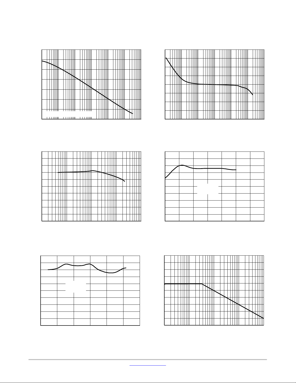
120
100
80
60
40
GAIN (dB)
20
0
Same Gain $1.8 dB (Typ)
−20
1k 10k 100k 1M 10M10010 1k 10k 100k 1M 10M10010
FREQUENCY (Hz)
Figure 1. Open Loop Frequency Response
(R
= 2 kW, TA = 255C, VS = 5 V)
L
100
90
80
70
60
50
40
CMRR (dB)
30
20
10
0
10 100 1k 10k 100k
FREQUENCY (Hz)
Figure 3. CMRR vs. Frequency
(R
= 5 kW, VS = 5 V)
L
170
150
130
110
90
70
PHASE MARGIN (°)
50
30
10
FREQUENCY (Hz)
Figure 2. Open Loop Phase Margin
(RL = 2 kW, TA = 255C, VS = 5 V)
80
75
70
65
60
55
50
CMRR (dB)
45
40
35
30
−0.5 0 0.5 1 1.5 2 2.5 3
INPUT COMMON MODE VOLTAGE (V)
VS = 2.7 V
f = 10 kHz
Figure 4. CMRR vs. Input Common Mode
Voltage
80
70
60
50
CMRR (dB)
40
30
−1012345
VS = 5 V
f = 10 kHz
INPUT COMMON MODE VOLTAGE (V)
Figure 5. CMRR vs. Input Common Mode
Voltage
www.onsemi.com
PSRR (dB)
6
100
90
80
70
60
50
40
30
20
10
0
1k 10k 100k 1M 10M
FREQUENCY (Hz)
Figure 6. PSRR vs. Frequency
= 5 kW, VS = 2.7 V, +PSRR)
(R
L
Page 7
LMV321, NCV321, LMV358, LMV324
TYPICAL CHARACTERISTICS
(TA = 25°C and VS = 5 V unless otherwise specified)
90
80
70
60
50
40
PSRR (dB)
30
20
10
0
1k 10k 100k 1M 10M
FREQUENCY (Hz)
Figure 7. PSRR vs. Frequency
(R
= 5 kW, VS = 2.7 V, −PSRR)
L
100
90
80
70
60
50
40
PSRR (dB)
30
20
10
0
1k 10k 100k 1M 10M
FREQUENCY (Hz)
Figure 9. PSRR vs. Frequency
(R
= 5 kW, VS = 5 V, −PSRR)
L
100
90
80
70
60
50
40
PSRR (dB)
30
20
10
0
1k 10k 100k 1M 10M
FREQUENCY (Hz)
Figure 8. PSRR vs. Frequency
(R
= 5 kW, VS = 5 V, +PSRR)
L
5
4.5
4
3.5
3
2.5
(mV)
OS
2
V
1.5
1
0.5
0
0 0.5 1 1.5 2 2.5 3
VS = 2.7 V
VCM (V)
Figure 10. VOS vs CMR
5
4.5
4
3.5
3
2.5
(mV)
OS
2
V
1.5
1
0.5
0
0 0.5 1 1.5 2 2.5 3 3.5 4 4.5 5
VS = 5.0 V
VCM (V)
Figure 11. VOS vs CMR
200
180
160
140
120
100
80
60
40
SUPPLY CURRENT (mA)
20
www.onsemi.com
7
0
0 0.5 1 1.5 2 2.5 3 3.5 4 4.5 5
SUPPLY VOLTAGE (V)
Figure 12. Supply Current vs. Supply Voltage
Page 8

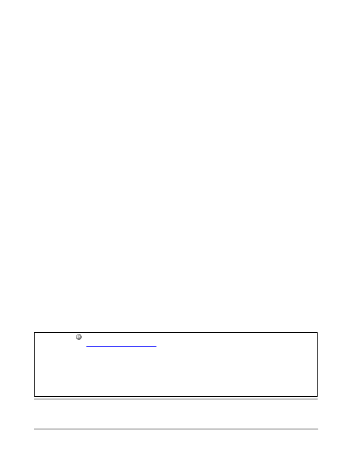
LMV321, NCV321, LMV358, LMV324
5
TYPICAL CHARACTERISTICS
(TA = 25°C and VS = 5 V unless otherwise specified)
1
RL = 10 kW
= 1 V
V
out
0.1
(%)
0.01
0.001
10 100 1k 10k 100k
PP
Av = +1
(Hz)
Figure 13. THD+N vs Frequency
0.1
0.09
0.08
0.07
0.06
0.05
0.04
0.03
REFERENCED TO V− (V)
0.02
OUT
V
0.01
0
2.5 3 3.5 4 4.5 5
Negative Swing
SUPPLY VOLTAGE (V)
Figure 15. Output Voltage Swing vs Supply
Voltage (R
= 10k)
L
0
−0.01
−0.02
−0.03
−0.04
−0.05
−0.06
−0.07
REFERENCED TO V+ (V)
−0.08
OUT
V
−0.09
−0.1
2.5 3 3.5 4 4.5
Positive Swing
SUPPLY VOLTAGE (V)
Figure 14. Output Voltage Swing vs Supply
Voltage (R
0
−20
−40
−60
−80
−100
−120
SINK CURRENT (mA)
−140
−160
0 0.5 1 1.5 2 2.5
V
REFERENCED TO V− (V)
OUT
= 10k)
L
Figure 16. Sink Current vs. Output Voltage
V
= 2.7 V
S
0
−20
−40
−60
−80
SINK CURRENT (mA)
−100
−120
012345
V
REFERENCED TO V− (V)
OUT
Figure 17. Sink Current vs. Output Voltage
= 5.0 V
V
S
www.onsemi.com
120
100
80
60
40
SOURCE CURRENT (mA)
20
0
0 0.5 1.0 1.5 2.0 2.5
Figure 18. Source Current vs. Output Voltage
8
V
REFERENCED TO V+ (V)
OUT
= 2.7 V
V
S
Page 9

LMV321, NCV321, LMV358, LMV324
TYPICAL CHARACTERISTICS
(TA = 25°C and VS = 5 V unless otherwise specified)
110
100
90
80
70
60
50
40
30
20
SOURCE CURRENT (mA)
10
0
012345
V
REFERENCED TO V+ (V)
OUT
Figure 19. Source Current vs. Output Voltage
V
= 5.0 V
S
RL = 1 MW
AV = 1
50 mV/div
2 ms/div
RL = 2 kW
AV = 1
50 mV/div
2 ms/div
Figure 20. Settling Time vs. Capacitive Load
50 mV/div
2 ms/div
Non−Inverting (G = +1)
Input
Figure 21. Settling Time vs. Capacitive Load
50 mV/div
2 ms/div
Inverting (G = −1)
Input
Output
Figure 23. Step Response − Small Signal
Output
Figure 22. Step Response − Small Signal
1 V/div
2 ms/div
Non−Inverting (G = +1)
Input
Output
Figure 24. Step Response − Large Signal
www.onsemi.com
9
Page 10

LMV321, NCV321, LMV358, LMV324
TYPICAL CHARACTERISTICS
(TA = 25°C and VS = 5 V unless otherwise specified)
1 V/div
2 ms/div
Inverting (G = −1)
Input
Output
Figure 25. Step Response − Large Signal
www.onsemi.com
10
Page 11

LMV321, NCV321, LMV358, LMV324
APPLICATIONS
50 k
R1
5.0 k
V
V
REF
CC
R2
2.5 V
CC
−
LMV321
+
VO+ 2.5 V(1 )
R1
R2
V
ref
V
O
1
+
ref
V
2
V
)
Figure 26. Voltage Reference Figure 27. Wien Bridge Oscillator
V
R2
Hysteresis
V
R1
V
ref
V
in
+
LMV321
−
VinL +
VinH +
H +
OH
V
V
O
V
OL
R1
R1 ) R2
R1
R1 ) R2
R1
R1 ) R2
O
(VOL* V
(VOH* V
(VOH* VOL)
V
inLVinH
V
ref
ref)
ref)
) V
) V
ref
ref
in
Given: f
Choose value f
Then : R3 +
Figure 28. Comparator with Hysteresis
For less than 10% error from operational amplifier,
((Q
O fO
If source impedance varies, filter may be preceded with
voltage follower buffer to stabilize filter parameters.
10 k
CC
R
C
R1
C
R2
= center frequency
o
) = gain at center frequency
A(f
o
, C
o
Q
C
pf
O
R1 +
R2 +
R3
2A(f
2
4Q
)
O
R1 R3
R1 * R3
−
LMV321
+
C
R3
V
ref
V
CC
R
V
CC
−
LMV321
+
V
O
fO+
2pRC
For: f
= 1.0 kHz
o
C
R = 16 kW
C = 0.01 mF
C
O
CO = 10 C
)/BW) < 0.1 where fo and BW are expressed in Hz.
1
V
O
www.onsemi.com
11
Figure 29. Multiple Feedback Bandpass Filter
Page 12

LMV321, NCV321, LMV358, LMV324
ORDERING INFORMATION
Number
of
Order Number
LMV321SQ3T2G Single AAC SC−70
LMV321SN3T1G Single 3AC TSOP−5
LMV321ISN3T1G Single 3AC TSOP−5
NCV321SN3T1G* Single 3AC TSOP−5
LMV358DMR2G Dual V358 Micro8
LMV358MUTAG Dual AC UDFN8
LMV358DR2G Dual V358 SOIC−8
LMV358IDR2G Dual V358 SOIC−8
LMV324DR2G Quad LMV324 SOIC−14
LMV324DTBR2G Quad LMV
†For information on tape and reel specifications, including part orientation and tape sizes, please refer to our Tape and Reel Packaging
Specifications Brochure, BRD8011/D.
*NCV Prefix for Automotive and Other Applications Requiring Unique Site and Control Change Requirements; AEC−Q100 Qualified and PPAP
Capable.
Channels
Specific Device Marking Package Type Shipping
3000 / Tape & Reel
3000 / Tape & Reel
3000 / Tape & Reel
3000 / Tape & Reel
4000 / Tape & Reel
3000 / Tape & Reel
2500 / Tape & Reel
2500 / Tape & Reel
2500 / Tape & Reel
2500 / Tape & Reel
324
(Pb−Free)
(Pb−Free)
(Pb−Free)
(Pb−Free)
(Pb−Free)
(Pb−Free)
(Pb−Free)
(Pb−Free)
(Pb−Free)
TSSOP−14
(Pb−Free)
†
www.onsemi.com
12
Page 13

MECHANICAL CASE OUTLINE
PACKAGE DIMENSIONS
SC−88A (SC−70−5/SOT−353)
SCALE 2:1
CASE 419A−02
ISSUE L
DATE 17 JAN 2013
S
0.40
0.0157
A
G
12 3
H
SOLDER FOOTPRINT
0.50
0.0197
D
NOTES:
1. DIMENSIONING AND TOLERANCING
PER ANSI Y14.5M, 1982.
2. CONTROLLING DIMENSION: INCH.
3. 419A−01 OBSOLETE. NEW STANDARD
419A−02.
4. DIMENSIONS A AND B DO NOT INCLUDE
45
−B−
MM
5 PL
B0.2 (0.008)
N
MOLD FLASH, PROTRUSIONS, OR GATE
BURRS.
INCHES
DIMAMIN MAX MIN MAX
B 1.15 1.350.045 0.053
C 0.80 1.100.031 0.043
D 0.10 0.300.004 0.012
G 0.65 BSC0.026 BSC
H --- 0.10---0.004
J 0.10 0.250.004 0.010
K 0.10 0.300.004 0.012
N 0.20 REF0.008 REF
S 2.00 2.200.079 0.087
MILLIMETERS
1.80 2.200.071 0.087
J
C
GENERIC MARKING
DIAGRAM*
K
XXXMG
G
XXX = Specific Device Code
M = Date Code
G = Pb−Free Package
0.65
0.025
0.65
0.025
(Note: Microdot may be in either location)
*This information is generic. Please refer to
device data sheet for actual part marking.
Pb−Free indicator, “G” or microdot “G”, may
or may not be present. Some products may
not follow the Generic Marking.
1.9
0.0748
STYLE 1:
PIN 1. BASE
2. EMITTER
3. BASE
4. COLLECTOR
5. COLLECTOR
STYLE 6:
PIN 1. EMITTER 2
2. BASE 2
3. EMITTER 1
4. COLLECTOR
5. COLLECTOR 2/BASE 1
DOCUMENT NUMBER:
DESCRIPTION:
ON Semiconductor and are trademarks of Semiconductor Components Industries, LLC dba ON Semiconductor or its subsidiaries in the United States and/or other countries.
ON Semiconductor reserves the right to make changes without further notice to any products herein. ON Semiconductor makes no warranty, representation or guarantee regarding
the suitability of its products for any particular purpose, nor does ON Semiconductor assume any liability arising out of the application or use of any product or circuit, and specifically
disclaims any and all liability, including without limitation special, consequential or incidental damages. ON Semiconductor does not convey any license under its patent rights nor the
rights of others.
© Semiconductor Components Industries, LLC, 2018
STYLE 2:
PIN 1. ANODE
2. EMITTER
3. BASE
4. COLLECTOR
5. CATHODE
STYLE 7:
PIN 1. BASE
2. EMITTER
3. BASE
4. COLLECTOR
5. COLLECTOR
98ASB42984B
SC−88A (SC−70−5/SOT−353)
SCALE 20:1
STYLE 3:
PIN 1. ANODE 1
STYLE 8:
PIN 1. CATHODE
mm
ǒ
Ǔ
inches
STYLE 4:
2. N/C
3. ANODE 2
4. CATHODE 2
5. CATHODE 1
2. COLLECTOR
3. N/C
4. BASE
5. EMITTER
Electronic versions are uncontrolled except when accessed directly from the Document Repository.
Printed versions are uncontrolled except when stamped “CONTROLLED COPY” in red.
PIN 1. SOURCE 1
2. DRAIN 1/2
3. SOURCE 1
4. GATE 1
5. GATE 2
STYLE 9:
PIN 1. ANODE
2. CATHODE
3. ANODE
4. ANODE
5. ANODE
STYLE 5:
PIN 1. CATHODE
2. COMMON ANODE
3. CATHODE 2
4. CATHODE 3
5. CATHODE 4
Note: Please refer to datasheet for
style callout. If style type is not called
out in the datasheet refer to the device
datasheet pinout or pin assignment.
PAGE 1 OF 1
www.onsemi.com
Page 14

MECHANICAL CASE OUTLINE
PACKAGE DIMENSIONS
5
1
SCALE 2:1
NOTE 5
2X
2X
T0.10
B
A
54
B
123
G
A
T0.20
TOP VIEW
0.05
H
SIDE VIEW
D
0.205XC AB
S
C
SEATING
C
PLANE
TSOP−5
CASE 483
ISSUE N
K
J
END VIEW
DETAIL Z
M
DETAIL Z
DATE 12 AUG 2020
NOTES:
1. DIMENSIONING AND TOLERANCING PER ASME
Y14.5M, 1994.
2. CONTROLLING DIMENSION: MILLIMETERS.
3. MAXIMUM LEAD THICKNESS INCLUDES LEAD FINISH
THICKNESS. MINIMUM LEAD THICKNESS IS THE
MINIMUM THICKNESS OF BASE MATERIAL.
4. DIMENSIONS A AND B DO NOT INCLUDE MOLD
FLASH, PROTRUSIONS, OR GATE BURRS. MOLD
FLASH, PROTRUSIONS, OR GATE BURRS SHALL NOT
EXCEED 0.15 PER SIDE. DIMENSION A.
5. OPTIONAL CONSTRUCTION: AN ADDITIONAL
TRIMMED LEAD IS ALLOWED IN THIS LOCATION.
TRIMMED LEAD NOT TO EXTEND MORE THAN 0.2
FROM BODY.
MILLIMETERS
DIM MIN MAX
A
2.85 3.15
B
1.35 1.65
C 0.90 1.10
D 0.25 0.50
G 0.95 BSC
H 0.01 0.10
J 0.10 0.26
K 0.20 0.60
M 0 10
__
S 2.50 3.00
SOLDERING FOOTPRINT*
1.9
0.95
0.037
1.0
0.039
*For additional information on our Pb−Free strategy and soldering
details, please download the ON Semiconductor Soldering and
Mounting Techniques Reference Manual, SOLDERRM/D.
0.074
0.028
0.7
2.4
0.094
SCALE 10:1
mm
ǒ
inches
GENERIC
MARKING DIAGRAM*
5
XXXAYWG
G
1
Analog
XXX = Specific Device Code
A = Assembly Location
Y = Year
W = Work Week
G = Pb−Free Package
(Note: Microdot may be in either location)
Ǔ
*This information is generic. Please refer to
device data sheet for actual part marking.
Pb−Free indicator, “G” or microdot “ G”,
may or may not be present.
5
XXX MG
G
1
Discrete/Logic
XXX = Specific Device Code
M = Date Code
G = Pb−Free Package
DOCUMENT NUMBER:
DESCRIPTION:
ON Semiconductor and are trademarks of Semiconductor Components Industries, LLC dba ON Semiconductor or its subsidiaries in the United States and/or other countries.
ON Semiconductor reserves the right to make changes without further notice to any products herein. ON Semiconductor makes no warranty, representation or guarantee regarding
the suitability of its products for any particular purpose, nor does ON Semiconductor assume any liability arising out of the application or use of any product or circuit, and specifically
disclaims any and all liability, including without limitation special, consequential or incidental damages. ON Semiconductor does not convey any license under its patent rights nor the
rights of others.
© Semiconductor Components Industries, LLC, 2018
98ARB18753C
TSOP−5
Electronic versions are uncontrolled except when accessed directly from the Document Repository.
Printed versions are uncontrolled except when stamped “CONTROLLED COPY” in red.
PAGE 1 OF 1
www.onsemi.com
Page 15

MECHANICAL CASE OUTLINE
PACKAGE DIMENSIONS
SCALE 4:1
0.10 C
PIN ONE
REFERENCE
0.05 C
0.05 C
(b2)
(L2)
8
1
0.10 C
TOP VIEW
SIDE VIEW
e/2
1
BOTTOM VIEW
UDFN8 1.8x1.2, 0.4P
CASE 517AJ−01
ISSUE O
DATE 08 NOV 2006
D
A B
L1
E
DETAIL A
NOTE 5
(A3)
A
A1
DETAIL A
e
4
SEATING
C
PLANE
8X
L
NOTES:
1. DIMENSIONING AND TOLERANCING PER
ASME Y14.5M, 1994.
2. CONTROLLING DIMENSION: MILLIMETERS.
3. DIMENSION b APPLIES TO PLATED
TERMINAL AND IS MEASURED BETWEEN
0.15 AND 0.30 mm FROM TERMINAL TIP.
4. MOLD FLASH ALLOWED ON TERMINALS
ALONG EDGE OF PACKAGE. FLASH MAY
NOT EXCEED 0.03 ONTO BOTTOM
SURFACE OF TERMINALS.
5. DETAIL A SHOWS OPTIONAL
CONSTRUCTION FOR TERMINALS.
MILLIMETERS
DIM MIN MAX
A 0.45 0.55
A1 0.00 0.05
A3 0.127 REF
b 0.15 0.25
b2 0.30 REF
D 1.80 BSC
E 1.20 BSC
e 0.40 BSC
L 0.45 0.55
L1 0.00 0.03
L2 0.40 REF
GENERIC
58
8X
b
0.10
0.05
M
M
C
BAC
NOTE 3
MARKING DIAGRAM*
XXM
G
MOUNTING FOOTPRINT
SOLDERMASK DEFINED
7X
0.22
1
0.32
DOCUMENT NUMBER:
DESCRIPTION:
8X
0.66
1.50
0.40 PITCH
DIMENSIONS: MILLIMETERS
98AON23417D
UDFN8 1.8X1.2, 0.4P
XX = Specific Device Code
M = Date Code
G = Pb−Free Package
*This information is generic. Please refer to
device data sheet for actual part marking.
Pb−Free indicator, “G” or microdot “ G”,
may or may not be present.
Electronic versions are uncontrolled except when accessed directly from the Document Repository.
Printed versions are uncontrolled except when stamped “CONTROLLED COPY” in red.
PAGE 1 OF 1
ON Semiconductor and are trademarks of Semiconductor Components Industries, LLC dba ON Semiconductor or its subsidiaries in the United States and/or other countries.
ON Semiconductor reserves the right to make changes without further notice to any products herein. ON Semiconductor makes no warranty, representation or guarantee regarding
the suitability of its products for any particular purpose, nor does ON Semiconductor assume any liability arising out of the application or use of any product or circuit, and specifically
disclaims any and all liability, including without limitation special, consequential or incidental damages. ON Semiconductor does not convey any license under its patent rights nor the
rights of others.
© Semiconductor Components Industries, LLC, 2019
www.onsemi.com
Page 16

MECHANICAL CASE OUTLINE
PACKAGE DIMENSIONS
8
1
SCALE 1:1
−Y−
−Z−
−X−
A
58
B
1
4
G
H
D
0.25 (0.010) Z
M
SOLDERING FOOTPRINT*
7.0
0.275
S
Y
SXS
0.25 (0.010)
C
SEATING
PLANE
1.52
0.060
0.155
0.10 (0.004)
4.0
CASE 751−07
M
M
Y
N
SOIC−8 NB
ISSUE AK
K
X 45
_
M
J
MARKING DIAGRAM*
8
XXXXX
ALYWX
1
XXXXX = Specific Device Code
A = Assembly Location
L = Wafer Lot
Y = Year
W = Work Week
G = Pb−Free Package
8
XXXXX
ALYWX
G
1
IC
IC
(Pb−Free)
DATE 16 FEB 2011
NOTES:
1. DIMENSIONING AND TOLERANCING PER
ANSI Y14.5M, 1982.
2. CONTROLLING DIMENSION: MILLIMETER.
3. DIMENSION A AND B DO NOT INCLUDE
MOLD PROTRUSION.
4. MAXIMUM MOLD PROTRUSION 0.15 (0.006)
PER SIDE.
5. DIMENSION D DOES NOT INCLUDE DAMBAR
PROTRUSION. ALLOWABLE DAMBAR
PROTRUSION SHALL BE 0.127 (0.005) TOTAL
IN EXCESS OF THE D DIMENSION AT
MAXIMUM MATERIAL CONDITION.
6. 751−01 THRU 751−06 ARE OBSOLETE. NEW
STANDARD IS 751−07.
MILLIMETERS
DIMAMIN MAX MIN MAX
4.80 5.00 0.189 0.197
B 3.80 4.00 0.150 0.157
C 1.35 1.75 0.053 0.069
D 0.33 0.51 0.013 0.020
G 1.27 BSC 0.050 BSC
H 0.10 0.25 0.004 0.010
J 0.19 0.25 0.007 0.010
K 0.40 1.27 0.016 0.050
M 0 8 0 8
____
N 0.25 0.50 0.010 0.020
S 5.80 6.20 0.228 0.244
INCHES
GENERIC
8
XXXXXX
AYWW
1
Discrete
XXXXXX = Specific Device Code
A = Assembly Location
Y = Year
WW = Work Week
G = Pb−Free Package
8
XXXXXX
AYWW
1
Discrete
(Pb−Free)
G
0.6
0.024
1.270
0.050
SCALE 6:1
ǒ
inches
mm
Ǔ
*This information is generic. Please refer to
device data sheet for actual part marking.
Pb−Free indicator, “G” or microdot “G”, may
or may not be present. Some products may
not follow the Generic Marking.
*For additional information on our Pb−Free strategy and soldering
details, please download the ON Semiconductor Soldering and
Mounting Techniques Reference Manual, SOLDERRM/D.
STYLES ON PAGE 2
DOCUMENT NUMBER:
DESCRIPTION:
ON Semiconductor and are trademarks of Semiconductor Components Industries, LLC dba ON Semiconductor or its subsidiaries in the United States and/or other countries.
ON Semiconductor reserves the right to make changes without further notice to any products herein. ON Semiconductor makes no warranty, representation or guarantee regarding
the suitability of its products for any particular purpose, nor does ON Semiconductor assume any liability arising out of the application or use of any product or circuit, and specifically
disclaims any and all liability, including without limitation special, consequential or incidental damages. ON Semiconductor does not convey any license under its patent rights nor the
rights of others.
© Semiconductor Components Industries, LLC, 2019
98ASB42564B
SOIC−8 NB
Electronic versions are uncontrolled except when accessed directly from the Document Repository.
Printed versions are uncontrolled except when stamped “CONTROLLED COPY” in red.
PAGE 1 OF 2
www.onsemi.com
Page 17

STYLE 1:
PIN 1. EMITTER
2. COLLECTOR
3. COLLECTOR
4. EMITTER
5. EMITTER
6. BASE
7. BASE
8. EMITTER
STYLE 5:
PIN 1. DRAIN
2. DRAIN
3. DRAIN
4. DRAIN
5. GATE
6. GATE
7. SOURCE
8. SOURCE
STYLE 9:
PIN 1. EMITTER, COMMON
2. COLLECTOR, DIE #1
3. COLLECTOR, DIE #2
4. EMITTER, COMMON
5. EMITTER, COMMON
6. BASE, DIE #2
7. BASE, DIE #1
8. EMITTER, COMMON
STYLE 13:
PIN 1. N.C.
2. SOURCE
3. SOURCE
4. GATE
5. DRAIN
6. DRAIN
7. DRAIN
8. DRAIN
STYLE 17:
PIN 1. VCC
2. V2OUT
3. V1OUT
4. TXE
5. RXE
6. VEE
7. GND
8. ACC
STYLE 21:
PIN 1. CATHODE 1
2. CATHODE 2
3. CATHODE 3
4. CATHODE 4
5. CATHODE 5
6. COMMON ANODE
7. COMMON ANODE
8. CATHODE 6
STYLE 25:
PIN 1. VIN
2. N/C
3. REXT
4. GND
5. IOUT
6. IOUT
7. IOUT
8. IOUT
STYLE 29:
PIN 1. BASE, DIE #1
2. EMITTER, #1
3. BASE, #2
4. EMITTER, #2
5. COLLECTOR, #2
6. COLLECTOR, #2
7. COLLECTOR, #1
8. COLLECTOR, #1
STYLE 2:
PIN 1. COLLECTOR, DIE, #1
2. COLLECTOR, #1
3. COLLECTOR, #2
4. COLLECTOR, #2
5. BASE, #2
6. EMITTER, #2
7. BASE, #1
8. EMITTER, #1
STYLE 6:
PIN 1. SOURCE
2. DRAIN
3. DRAIN
4. SOURCE
5. SOURCE
6. GATE
7. GATE
8. SOURCE
STYLE 10:
PIN 1. GROUND
2. BIAS 1
3. OUTPUT
4. GROUND
5. GROUND
6. BIAS 2
7. INPUT
8. GROUND
STYLE 14:
PIN 1. N−SOURCE
2. N−GATE
3. P−SOURCE
4. P−GATE
5. P−DRAIN
6. P−DRAIN
7. N−DRAIN
8. N−DRAIN
STYLE 18:
PIN 1. ANODE
2. ANODE
3. SOURCE
4. GATE
5. DRAIN
6. DRAIN
7. CATHODE
8. CATHODE
STYLE 22:
PIN 1. I/O LINE 1
2. COMMON CATHODE/VCC
3. COMMON CATHODE/VCC
4. I/O LINE 3
5. COMMON ANODE/GND
6. I/O LINE 4
7. I/O LINE 5
8. COMMON ANODE/GND
STYLE 26:
PIN 1. GND
2. dv/dt
3. ENABLE
4. ILIMIT
5. SOURCE
6. SOURCE
7. SOURCE
8. VCC
STYLE 30:
PIN 1. DRAIN 1
2. DRAIN 1
3. GATE 2
4. SOURCE 2
5. SOURCE 1/DRAIN 2
6. SOURCE 1/DRAIN 2
7. SOURCE 1/DRAIN 2
8. GATE 1
SOIC−8 NB
CASE 751−07
ISSUE AK
STYLE 3:
STYLE 7:
STYLE 11:
STYLE 15:
STYLE 19:
STYLE 23:
PIN 1. DRAIN, DIE #1
2. DRAIN, #1
3. DRAIN, #2
4. DRAIN, #2
5. GATE, #2
6. SOURCE, #2
7. GATE, #1
8. SOURCE, #1
PIN 1. INPUT
2. EXTERNAL BYPASS
3. THIRD STAGE SOURCE
4. GROUND
5. DRAIN
6. GATE 3
7. SECOND STAGE Vd
8. FIRST STAGE Vd
PIN 1. SOURCE 1
2. GATE 1
3. SOURCE 2
4. GATE 2
5. DRAIN 2
6. DRAIN 2
7. DRAIN 1
8. DRAIN 1
PIN 1. ANODE 1
2. ANODE 1
3. ANODE 1
4. ANODE 1
5. CATHODE, COMMON
6. CATHODE, COMMON
7. CATHODE, COMMON
8. CATHODE, COMMON
PIN 1. SOURCE 1
2. GATE 1
3. SOURCE 2
4. GATE 2
5. DRAIN 2
6. MIRROR 2
7. DRAIN 1
8. MIRROR 1
PIN 1. LINE 1 IN
2. COMMON ANODE/GND
3. COMMON ANODE/GND
4. LINE 2 IN
5. LINE 2 OUT
6. COMMON ANODE/GND
7. COMMON ANODE/GND
8. LINE 1 OUT
STYLE 27:
PIN 1. ILIMIT
2. OVLO
3. UVLO
4. INPUT+
5. SOURCE
6. SOURCE
7. SOURCE
8. DRAIN
DATE 16 FEB 2011
STYLE 4:
PIN 1. ANODE
2. ANODE
3. ANODE
4. ANODE
5. ANODE
6. ANODE
7. ANODE
8. COMMON CATHODE
STYLE 8:
PIN 1. COLLECTOR, DIE #1
2. BASE, #1
3. BASE, #2
4. COLLECTOR, #2
5. COLLECTOR, #2
6. EMITTER, #2
7. EMITTER, #1
8. COLLECTOR, #1
STYLE 12:
PIN 1. SOURCE
2. SOURCE
3. SOURCE
4. GATE
5. DRAIN
6. DRAIN
7. DRAIN
8. DRAIN
STYLE 16:
PIN 1. EMITTER, DIE #1
2. BASE, DIE #1
3. EMITTER, DIE #2
4. BASE, DIE #2
5. COLLECTOR, DIE #2
6. COLLECTOR, DIE #2
7. COLLECTOR, DIE #1
8. COLLECTOR, DIE #1
STYLE 20:
PIN 1. SOURCE (N)
2. GATE (N)
3. SOURCE (P)
4. GATE (P)
5. DRAIN
6. DRAIN
7. DRAIN
8. DRAIN
STYLE 24:
PIN 1. BASE
2. EMITTER
3. COLLECTOR/ANODE
4. COLLECTOR/ANODE
5. CATHODE
6. CATHODE
7. COLLECTOR/ANODE
8. COLLECTOR/ANODE
STYLE 28:
PIN 1. SW_TO_GND
2. DASIC_OFF
3. DASIC_SW_DET
4. GND
5. V_MON
6. VBULK
7. VBULK
8. VIN
DOCUMENT NUMBER:
DESCRIPTION:
ON Semiconductor and are trademarks of Semiconductor Components Industries, LLC dba ON Semiconductor or its subsidiaries in the United States and/or other countries.
ON Semiconductor reserves the right to make changes without further notice to any products herein. ON Semiconductor makes no warranty, representation or guarantee regarding
the suitability of its products for any particular purpose, nor does ON Semiconductor assume any liability arising out of the application or use of any product or circuit, and specifically
disclaims any and all liability, including without limitation special, consequential or incidental damages. ON Semiconductor does not convey any license under its patent rights nor the
rights of others.
© Semiconductor Components Industries, LLC, 2019
98ASB42564B
SOIC−8 NB
Electronic versions are uncontrolled except when accessed directly from the Document Repository.
Printed versions are uncontrolled except when stamped “CONTROLLED COPY” in red.
PAGE 2 OF 2
www.onsemi.com
Page 18

MECHANICAL CASE OUTLINE
PACKAGE DIMENSIONS
14
1
SCALE 1:1
SOIC−14 NB
CASE 751A−03
ISSUE L
DATE 03 FEB 2016
14
H
M
0.25 B
0.10
14X
0.58
D
M
13X
e
SOLDERING FOOTPRINT*
6.50
1
A
B
8
E
71
b
S
M
0.25 B
A
C
A
A1
SEATING
C
PLANE
1.18
14X
S
1.27
PITCH
DETAIL A
h
X 45
_
M
NOTES:
1. DIMENSIONING AND TOLERANCING PER
ASME Y14.5M, 1994.
2. CONTROLLING DIMENSION: MILLIMETERS.
3. DIMENSION b DOES NOT INCLUDE DAMBAR
A3
L
DETAIL A
PROTRUSION. ALLOWABLE PROTRUSION
SHALL BE 0.13 TOTAL IN EXCESS OF AT
MAXIMUM MATERIAL CONDITION.
4. DIMENSIONS D AND E DO NOT INCLUDE
MOLD PROTRUSIONS.
5. MAXIMUM MOLD PROTRUSION 0.15 PER
SIDE.
DIM MIN MAX MIN MAX
A 1.35 1.75 0.054 0.068
A1 0.10 0.25 0.004 0.010
A3 0.19 0.25 0.008 0.010
b 0.35 0.49 0.014 0.019
D 8.55 8.75 0.337 0.344
E 3.80 4.00 0.150 0.157
e 1.27 BSC 0.050 BSC
H 5.80 6.20 0.228 0.244
h 0.25 0.50 0.010 0.019
L 0.40 1.25 0.016 0.049
M 0 7 0 7
__ __
INCHESMILLIMETERS
GENERIC
MARKING DIAGRAM*
14
XXXXXXXXXG
AWLYWW
1
XXXXX = Specific Device Code
A = Assembly Location
WL = Wafer Lot
Y = Year
WW = Work Week
G = Pb−Free Package
*This information is generic. Please refer to
device data sheet for actual part marking.
Pb−Free indicator, “G” or microdot “ G”,
may or may not be present.
DIMENSIONS: MILLIMETERS
*For additional information on our Pb−Free strategy and soldering
details, please download the ON Semiconductor Soldering and
Mounting Techniques Reference Manual, SOLDERRM/D.
STYLES ON PAGE 2
DOCUMENT NUMBER:
DESCRIPTION:
ON Semiconductor and are trademarks of Semiconductor Components Industries, LLC dba ON Semiconductor or its subsidiaries in the United States and/or other countries.
ON Semiconductor reserves the right to make changes without further notice to any products herein. ON Semiconductor makes no warranty, representation or guarantee regarding
the suitability of its products for any particular purpose, nor does ON Semiconductor assume any liability arising out of the application or use of any product or circuit, and specifically
disclaims any and all liability, including without limitation special, consequential or incidental damages. ON Semiconductor does not convey any license under its patent rights nor the
rights of others.
© Semiconductor Components Industries, LLC, 2019
98ASB42565B
SOIC−14 NB
Electronic versions are uncontrolled except when accessed directly from the Document Repository.
Printed versions are uncontrolled except when stamped “CONTROLLED COPY” in red.
PAGE 1 OF 2
www.onsemi.com
Page 19

SOIC−14
CASE 751A−03
ISSUE L
DATE 03 FEB 2016
STYLE 1:
PIN 1. COMMON CATHODE
2. ANODE/CATHODE
3. ANODE/CATHODE
4. NO CONNECTION
5. ANODE/CATHODE
6. NO CONNECTION
7. ANODE/CATHODE
8. ANODE/CATHODE
9. ANODE/CATHODE
10. NO CONNECTION
11. ANODE/CATHODE
12. ANODE/CATHODE
13. NO CONNECTION
14. COMMON ANODE
STYLE 5:
PIN 1. COMMON CATHODE
2. ANODE/CATHODE
3. ANODE/CATHODE
4. ANODE/CATHODE
5. ANODE/CATHODE
6. NO CONNECTION
7. COMMON ANODE
8. COMMON CATHODE
9. ANODE/CATHODE
10. ANODE/CATHODE
11. ANODE/CATHODE
12. ANODE/CATHODE
13. NO CONNECTION
14. COMMON ANODE
STYLE 2:
CANCELLED
STYLE 6:
PIN 1. CATHODE
2. CATHODE
3. CATHODE
4. CATHODE
5. CATHODE
6. CATHODE
7. CATHODE
8. ANODE
9. ANODE
10. ANODE
11. ANODE
12. ANODE
13. ANODE
14. ANODE
STYLE 3:
PIN 1. NO CONNECTION
2. ANODE
3. ANODE
4. NO CONNECTION
5. ANODE
6. NO CONNECTION
7. ANODE
8. ANODE
9. ANODE
10. NO CONNECTION
11. ANODE
12. ANODE
13. NO CONNECTION
14. COMMON CATHODE
STYLE 7:
PIN 1. ANODE/CATHODE
2. COMMON ANODE
3. COMMON CATHODE
4. ANODE/CATHODE
5. ANODE/CATHODE
6. ANODE/CATHODE
7. ANODE/CATHODE
8. ANODE/CATHODE
9. ANODE/CATHODE
10. ANODE/CATHODE
11. COMMON CATHODE
12. COMMON ANODE
13. ANODE/CATHODE
14. ANODE/CATHODE
STYLE 4:
PIN 1. NO CONNECTION
2. CATHODE
3. CATHODE
4. NO CONNECTION
5. CATHODE
6. NO CONNECTION
7. CATHODE
8. CATHODE
9. CATHODE
10. NO CONNECTION
11. CATHODE
12. CATHODE
13. NO CONNECTION
14. COMMON ANODE
STYLE 8:
PIN 1. COMMON CATHODE
2. ANODE/CATHODE
3. ANODE/CATHODE
4. NO CONNECTION
5. ANODE/CATHODE
6. ANODE/CATHODE
7. COMMON ANODE
8. COMMON ANODE
9. ANODE/CATHODE
10. ANODE/CATHODE
11. NO CONNECTION
12. ANODE/CATHODE
13. ANODE/CATHODE
14. COMMON CATHODE
DOCUMENT NUMBER:
DESCRIPTION:
ON Semiconductor and are trademarks of Semiconductor Components Industries, LLC dba ON Semiconductor or its subsidiaries in the United States and/or other countries.
ON Semiconductor reserves the right to make changes without further notice to any products herein. ON Semiconductor makes no warranty, representation or guarantee regarding
the suitability of its products for any particular purpose, nor does ON Semiconductor assume any liability arising out of the application or use of any product or circuit, and specifically
disclaims any and all liability, including without limitation special, consequential or incidental damages. ON Semiconductor does not convey any license under its patent rights nor the
rights of others.
© Semiconductor Components Industries, LLC, 2019
98ASB42565B
SOIC−14 NB
Electronic versions are uncontrolled except when accessed directly from the Document Repository.
Printed versions are uncontrolled except when stamped “CONTROLLED COPY” in red.
PAGE 2 OF 2
www.onsemi.com
Page 20

MECHANICAL CASE OUTLINE
PACKAGE DIMENSIONS
SCALE 2:1
Micro8
CASE 846A−02
ISSUE K
DATE 16 JUL 2020
GENERIC
MARKING DIAGRAM*
8
XXXX
AYW G
G
1
XXXX = Specific Device Code
A = Assembly Location
Y = Year
W = Work Week
G = Pb−Free Package
(Note: Microdot may be in either location)
*This information is generic. Please refer to
device data sheet for actual part marking.
Pb−Free indicator, “G” or microdot “G”, may
or may not be present. Some products may
not follow the Generic Marking.
STYLE 1:
PIN 1. SOURCE
2. SOURCE
3. SOURCE
4. GATE
5. DRAIN
6. DRAIN
7. DRAIN
8. DRAIN
STYLE 2:
PIN 1. SOURCE 1
2. GATE 1
3. SOURCE 2
4. GATE 2
5. DRAIN 2
6. DRAIN 2
7. DRAIN 1
8. DRAIN 1
STYLE 3:
PIN 1. N-SOURCE
2. N-GATE
3. P-SOURCE
4. P-GATE
5. P-DRAIN
6. P-DRAIN
7. N-DRAIN
8. N-DRAIN
DOCUMENT NUMBER:
DESCRIPTION:
ON Semiconductor and are trademarks of Semiconductor Components Industries, LLC dba ON Semiconductor or its subsidiaries in the United States and/or other countries.
ON Semiconductor reserves the right to make changes without further notice to any products herein. ON Semiconductor makes no warranty, representation or guarantee regarding
the suitability of its products for any particular purpose, nor does ON Semiconductor assume any liability arising out of the application or use of any product or circuit, and specifically
disclaims any and all liability, including without limitation special, consequential or incidental damages. ON Semiconductor does not convey any license under its patent rights nor the
rights of others.
© Semiconductor Components Industries, LLC, 2019
98ASB14087C
MICRO8
Electronic versions are uncontrolled except when accessed directly from the Document Repository.
Printed versions are uncontrolled except when stamped “CONTROLLED COPY” in red.
PAGE 1 OF 1
www.onsemi.com
Page 21

MECHANICAL CASE OUTLINE
PACKAGE DIMENSIONS
14
1
SCALE 2:1
0.10 (0.004)
SEATING
−T−
PLANE
S
U0.15 (0.006) T
2X L/2
L
PIN 1
IDENT.
S
U0.15 (0.006) T
C
D
SOLDERING FOOTPRINT
1
14X REFK
0.10 (0.004) V
14
1
M
8
7
A
−V−
G
7.06
TSSOP−14 WB
S
U
T
B
N
−U−
J
H
CASE 948G
ISSUE C
S
N
F
DETAIL E
J1
SECTION N−N
DETAIL E
0.25 (0.010)
M
K
K1
DATE 17 FEB 2016
NOTES:
1. DIMENSIONING AND TOLERANCING PER
ANSI Y14.5M, 1982.
2. CONTROLLING DIMENSION: MILLIMETER.
3. DIMENSION A DOES NOT INCLUDE MOLD
FLASH, PROTRUSIONS OR GATE BURRS.
MOLD FLASH OR GATE BURRS SHALL NOT
EXCEED 0.15 (0.006) PER SIDE.
4. DIMENSION B DOES NOT INCLUDE
INTERLEAD FLASH OR PROTRUSION.
INTERLEAD FLASH OR PROTRUSION SHALL
NOT EXCEED 0.25 (0.010) PER SIDE.
5. DIMENSION K DOES NOT INCLUDE DAMBAR
PROTRUSION. ALLOWABLE DAMBAR
PROTRUSION SHALL BE 0.08 (0.003) TOTAL
IN EXCESS OF THE K DIMENSION AT
MAXIMUM MATERIAL CONDITION.
6. TERMINAL NUMBERS ARE SHOWN FOR
REFERENCE ONLY.
7. DIMENSION A AND B ARE TO BE
DETERMINED AT DATUM PLANE −W−.
INCHESMILLIMETERS
−W−
DIM MIN MAX MIN MAX
A 4.90 5.10 0.193 0.200
B 4.30 4.50 0.169 0.177
C −−− 1.20 −−− 0.047
D 0.05 0.15 0.002 0.006
F 0.50 0.75 0.020 0.030
G 0.65 BSC 0.026 BSC
H 0.50 0.60 0.020 0.024
J 0.09 0.20 0.004 0.008
J1 0.09 0.16 0.004 0.006
K 0.19 0.30 0.007 0.012
K1 0.19 0.25 0.007 0.010
L 6.40 BSC 0.252 BSC
M 0 8 0 8
____
GENERIC
MARKING DIAGRAM*
14
XXXX
XXXX
ALYWG
G
1
A = Assembly Location
L = Wafer Lot
Y = Year
0.65
PITCH
W = Work Week
G = Pb−Free Package
(Note: Microdot may be in either location)
*This information is generic. Please refer to
14X
0.36
DOCUMENT NUMBER:
DESCRIPTION:
ON Semiconductor and are trademarks of Semiconductor Components Industries, LLC dba ON Semiconductor or its subsidiaries in the United States and/or other countries.
ON Semiconductor reserves the right to make changes without further notice to any products herein. ON Semiconductor makes no warranty, representation or guarantee regarding
the suitability of its products for any particular purpose, nor does ON Semiconductor assume any liability arising out of the application or use of any product or circuit, and specifically
disclaims any and all liability, including without limitation special, consequential or incidental damages. ON Semiconductor does not convey any license under its patent rights nor the
rights of others.
© Semiconductor Components Industries, LLC, 2019
14X
1.26
98ASH70246A
TSSOP−14 WB
DIMENSIONS: MILLIMETERS
Electronic versions are uncontrolled except when accessed directly from the Document Repository.
Printed versions are uncontrolled except when stamped “CONTROLLED COPY” in red.
device data sheet for actual part marking.
Pb−Free indicator, “G” or microdot “ G”,
may or may not be present.
PAGE 1 OF 1
www.onsemi.com
Page 22
ON Semiconductor and are trademarks of Semiconductor Components Industries, LLC dba ON Semiconductor or its subsidiaries in the United States and/or other countries.
ON Semiconductor owns the rights to a number of patents, trademarks, copyrights, trade secrets, and other intellectual property. A listing of ON Semiconductor ’s product/patent
coverage may be accessed at www.onsemi.com/site/pdf/Patent−Marking.pdf
ON Semiconductor makes no warranty, representation or guarantee regarding the suitability of its products for any particular purpose, nor does ON Semiconductor assume any liability
arising out of the application or use of any product or circuit, and specifically disclaims any and all liability, including without limitation special, consequential or incidental damages.
Buyer is responsible for its products and applications using ON Semiconductor products, including compliance with all laws, regulations and safety requirements or standards,
regardless of any support or applications information provided by ON Semiconductor. “Typical” parameters which may be provided in ON Semiconductor data sheets and/or
specifications can and do vary in different applications and actual performance may vary over time. All operating parameters, including “Typicals” must be validated for each customer
application by customer’s technical experts. ON Semiconductor does not convey any license under its patent rights nor the rights of others. ON Semiconductor products are not
designed, intended, or authorized for use as a critical component in life support systems or any FDA Class 3 medical devices or medical devices with a same or similar classification
in a foreign jurisdiction or any devices intended for implantation in the human body. Should Buyer purchase or use ON Semiconductor products for any such unintended or unauthorized
application, Buyer shall indemnify and hold ON Semiconductor and its officers, employees, subsidiaries, affiliates, and distributors harmless against all claims, costs, damages, and
expenses, and reasonable attorney fees arising out of, directly or indirectly, any claim of personal injury or death associated with such unintended or unauthorized use, even if such
claim alleges that ON Semiconductor was negligent regarding the design or manufacture of the part. ON Semiconductor is an Equal Opportunity/Affirmative Action Employer. This
literature is subject to all applicable copyright laws and is not for resale in any manner.
. ON Semiconductor reserves the right to make changes without further notice to any products herein.
PUBLICATION ORDERING INFORMATION
LITERATURE FULFILLMENT:
Email Requests to: orderlit@onsemi.com
ON Semiconductor Website: www.onsemi.com
TECHNICAL SUPPORT
North American Technical Support:
Voice Mail: 1 800−282−9855 Toll Free USA/Canada
Phone: 011 421 33 790 2910
Europe, Middle East and Africa Technical Support:
Phone: 00421 33 790 2910
For additional information, please contact your local Sales Representative
◊
www.onsemi.com
1
 Loading...