

Page 1
LM2575
1.0 A, Adjustable Output
Voltage, Step−Down
Switching Regulator
The LM2575 series of regulators are monolithic integrated circuits
ideally suited for easy and convenient design of a step−down
switching regulator (buck converter). All circuits of this series are
capable of driving a 1.0 A load with excellent line and load regulation.
These devices are available in fixed output voltages of 3.3 V, 5.0 V,
12 V, 15 V, and an adjustable output version.
These regulators were designed to minimize the number of external
components to simplify the power supply design. Standard series of
inductors optimized for use with the LM2575 are offered by several
different inductor manufacturers.
Since the LM2575 converter is a switch−mode power supply, its
efficiency is significantly higher in comparison with popular
three−terminal linear regulators, especially with higher input voltages.
In many cases, the power dissipated by the LM2575 regulator is so
low, that no heatsink is required or its size could be reduced
dramatically.
The LM2575 features include a guaranteed ±4% tolerance on output
voltage within specified input voltages and output load conditions, and
±10% on the oscillator frequency (±2% over 0°C to 125°C). External
shutdown is included, featuring 80 mA typical standby current. The
output switch includes cycle−by−cycle current limiting, as well as
thermal shutdown for full protection under fault conditions.
Features
• 3.3 V, 5.0 V, 12 V, 15 V, and Adjustable Output Versions
• Adjustable Version Output Voltage Range of 1.23 V to 37 V ±4%
Maximum Over Line and Load Conditions
• Guaranteed 1.0 A Output Current
• Wide Input Voltage Range: 4.75 V to 40 V
• Requires Only 4 External Components
• 52 kHz Fixed Frequency Internal Oscillator
• TTL Shutdown Capability, Low Power Standby Mode
• High Efficiency
• Uses Readily Available Standard Inductors
• Thermal Shutdown and Current Limit Protection
• Moisture Sensitivity Level (MSL) Equals 1
• Pb−Free Packages are Available*
Applications
• Simple and High−Efficiency Step−Down (Buck) Regulators
• Efficient Pre−Regulator for Linear Regulators
• On−Card Switching Regulators
• Positive to Negative Converters (Buck−Boost)
• Negative Step−Up Converters
• Power Supply for Battery Chargers
http://onsemi.com
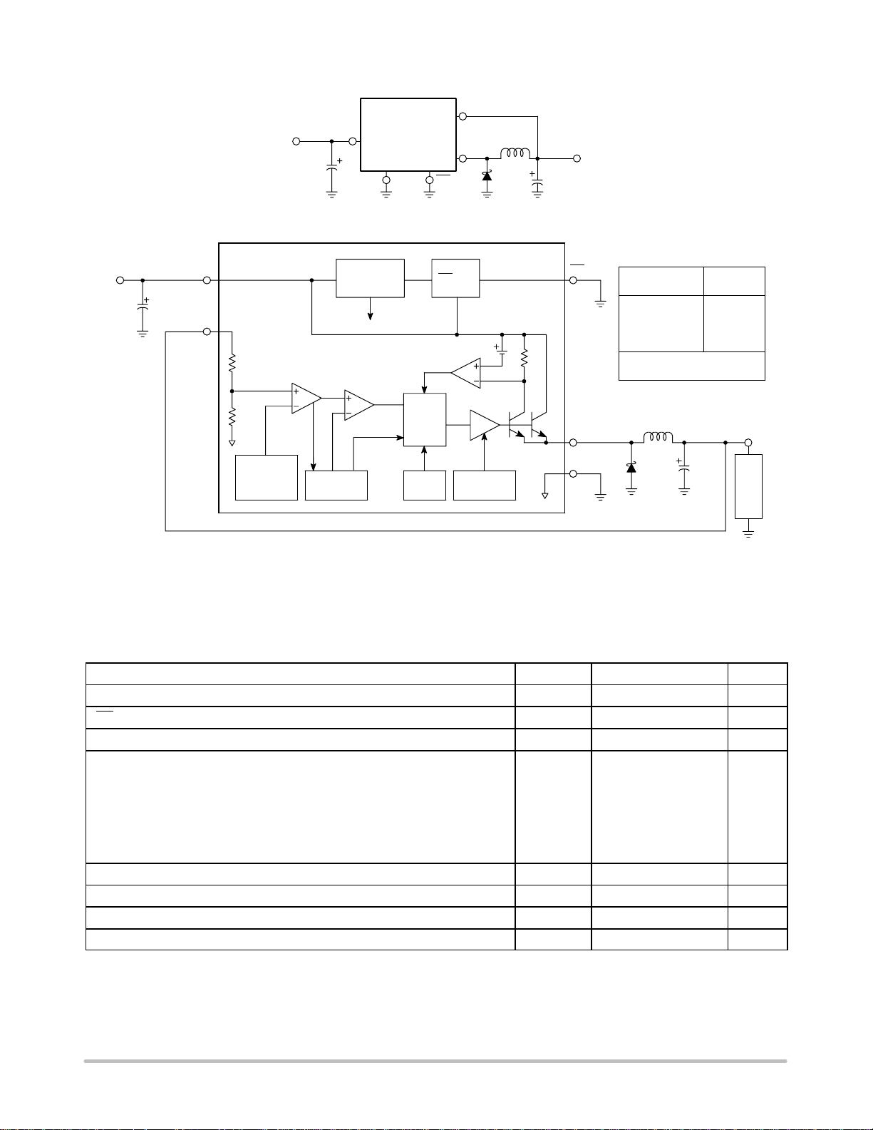
TO−220
1
5
Heatsink surface connected to Pin 3
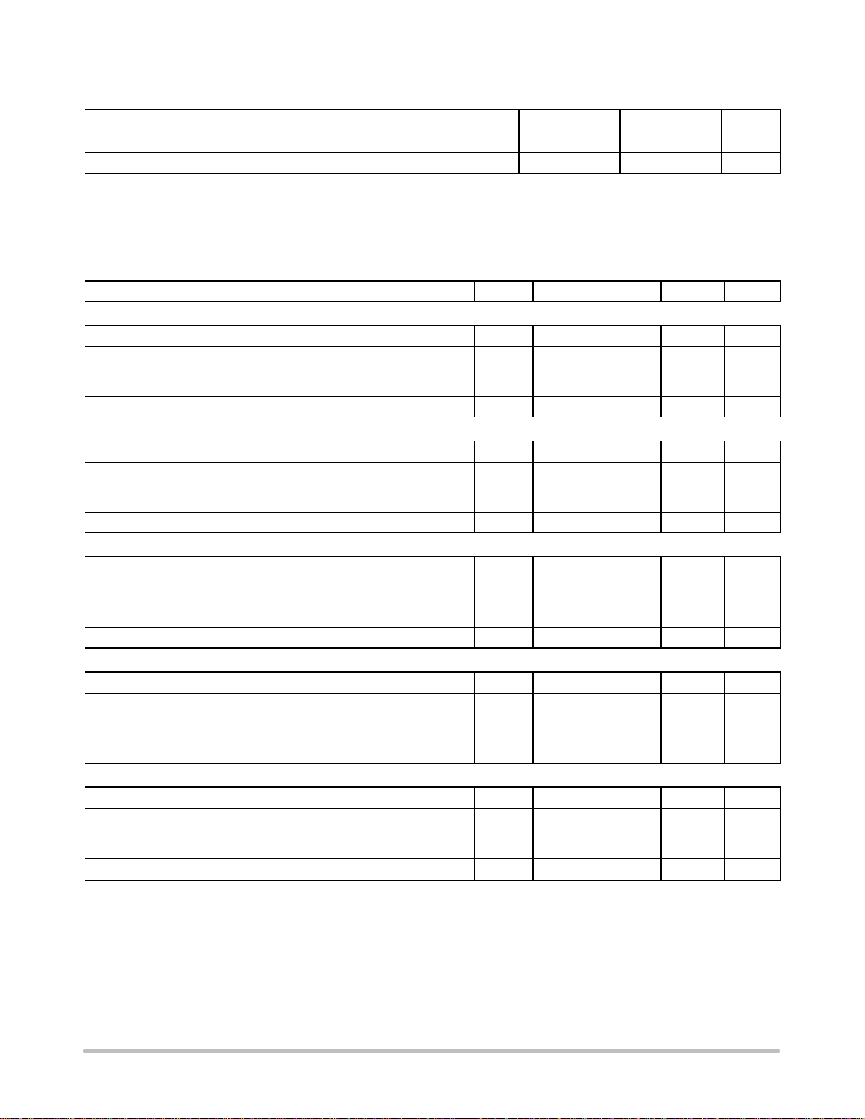
1
5
Pin 1. V
2. Output
3. Ground
4. Feedback
5. ON/OFF
1
5
Heatsink surface (shown as terminal 6 in
case outline drawing) is connected to Pin 3
ORDERING INFORMATION
See detailed ordering and shipping information in the package
dimensions section on page 24 of this data sheet.
DEVICE MARKING INFORMATION
See general marking information in the device marking
section on page 25 of this data sheet.
TV SUFFIX
CASE 314B
TO−220
T SUFFIX
CASE 314D
in
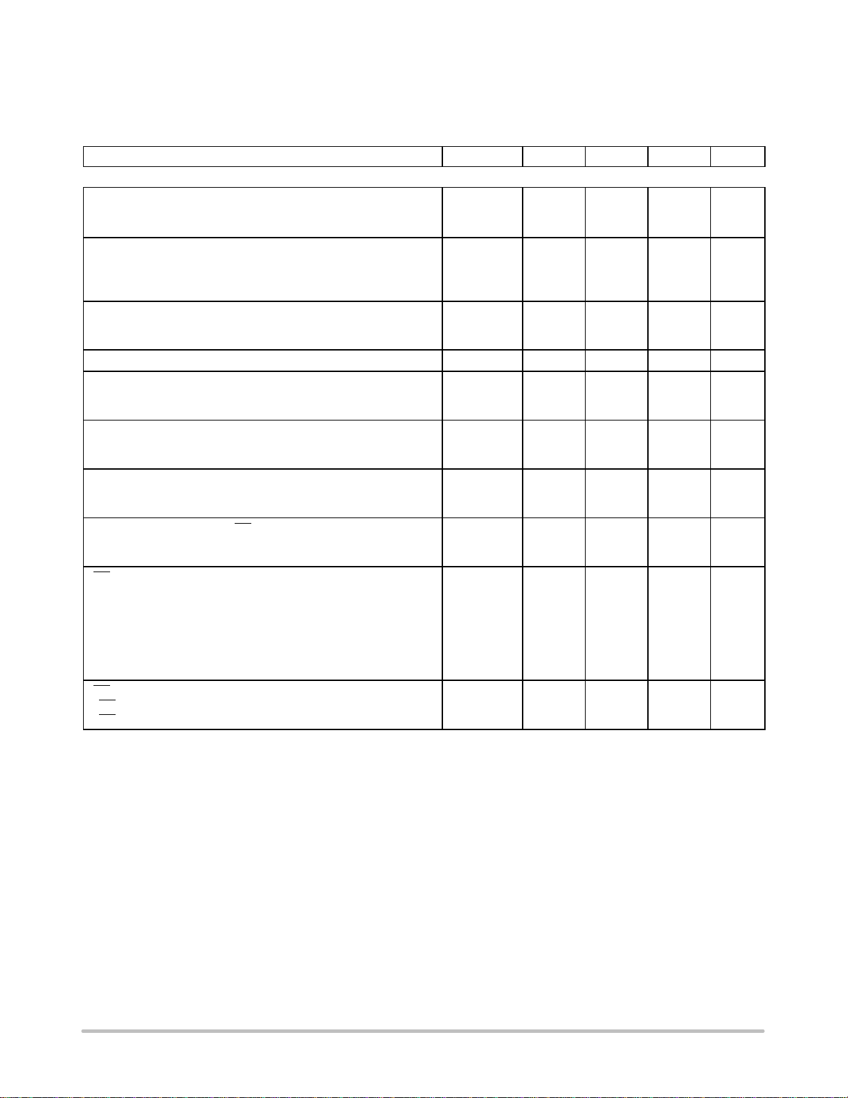
D2PAK
D2T SUFFIX
CASE 936A
*For additional information on our Pb−Free strategy and soldering details, please
download the ON Semiconductor Soldering and Mounting Techniques
Reference Manual, SOLDERRM/D.
© Semiconductor Components Industries, LLC, 2005
November, 2005 − Rev. 8
1 Publication Order Number:
LM2575/D
Page 2
Typical Application (Fixed Output Voltage Versions)
Unregulated
DC Input
C
in
+V
Feedback
in
1
4
LM2575
Feedback
L1
330 mH
D1
1N5819
Driver
1.0 Amp
Switch
Thermal
/OFF5
4
Output
2
7.0 V − 40 V
Unregulated
DC Input
C
100 mF
+V
in
LM2575
1
in
GND
3ON
Representative Block Diagram and Typical Application
R2
R1
1.0 k
1.235 V
Band−Gap
Reference
Fixed Gain
Error Amplifier
Freq
Shift
18 kHz
Oscillator
3.1 V Internal
Regulator
Comparator
52 kHz
Current
Latch
Reset
ON/OFF
Limit
Shutdown
C
out
330 mF
ON/OFF
5
Output
2
GND
3
5.0 V Regulated
Output 1.0 A Load
Output
Voltage Versions
3.3 V
5.0 V
12 V
15 V
For adjustable version
R1 = open, R2 = 0 W
D1
R2
(W)
1.7 k
3.1 k
8.84 k
11.3 k
Regulated
L1
Output
V
out
C
out
Load
This device contains 162 active transistors.
Figure 1. Block Diagram and Typical Application
ABSOLUTE MAXIMUM RATINGS (Absolute Maximum Ratings indicate limits beyond which damage to the device may occur.)
Rating Symbol Value Unit
Maximum Supply Voltage V
in
ON/OFF Pin Input Voltage − −0.3 V ≤ V ≤ +V
Output Voltage to Ground (Steady−State) − −1.0 V
Power Dissipation
Case 314B and 314D (TO−220, 5−Lead) P
Thermal Resistance, Junction−to−Ambient
Thermal Resistance, Junction−to−Case
Case 936A (D2PAK) P
Thermal Resistance, Junction−to−Ambient (Figure 34)
Thermal Resistance, Junction−to−Case
Storage Temperature Range T
Minimum ESD Rating (Human Body Model: C = 100 pF, R = 1.5 kW)
D
R
q
JA
R
q
JC
D
R
q
JA
R
q
JC
stg
− 3.0 kV
Lead Temperature (Soldering, 10 s) − 260 °C
Maximum Junction Temperature T
J
Maximum ratings are those values beyond which device damage can occur. Maximum ratings applied to the device are individual stress limit
values (not normal operating conditions) and are not valid simultaneously. If these limits are exceeded, device functional operation is not implied,
damage may occur and reliability may be affected.
45 V
in
Internally Limited W
65 °C/W
5.0 °C/W
Internally Limited W
70 °C/W
5.0 °C/W
−65 to +150 °C
150 °C
V
http://onsemi.com
2
Page 3
LM2575
OPERATING RATINGS (Operating Ratings indicate conditions for which the device is intended to be functional, but do not guarantee
specific performance limits. For guaranteed specifications and test conditions, see the Electrical Characteristics.)
Rating Symbol Value Unit
Operating Junction Temperature Range T
Supply Voltage V
J
in
SYSTEM PARAMETERS ([Note 1] Test Circuit Figure 14)
ELECTRICAL CHARACTERISTICS (Unless otherwise specified, V
for the 12 V version, and Vin = 30 V for the 15 V version. I
operating junction temperature range that applies [Note 2], unless otherwise noted.)
Characteristics Symbol Min Typ Max Unit
LM2575−3.3 (Note 1 Test Circuit Figure 14)
Output Voltage (Vin = 12 V, I
= 0.2 A, T
Load
Output Voltage (4.75 V ≤ Vin ≤ 40 V, 0.2 A ≤ I
= 25°C) V
J
≤ 1.0 A) V
Load
TJ = 25°C 3.168 3.3 3.432
TJ = −40 to +125°C 3.135 − 3.465
Efficiency (V
= 12 V, I
in
= 1.0 A) η − 75 − %
Load
LM2575−5 ([Note 1] Test Circuit Figure 14)
Output Voltage (Vin = 12 V, I
Output Voltage (8.0 V ≤ Vin ≤ 40 V, 0.2 A ≤ I
= 0.2 A, TJ = 25°C) V
Load
≤ 1.0 A) V
Load
TJ = 25°C 4.8 5.0 5.2
TJ = −40 to +125°C 4.75 − 5.25
Efficiency (Vin = 12 V, I
= 1.0 A) η − 77 − %
Load
LM2575−12 (Note 1 Test Circuit Figure 14)
Output Voltage (Vin = 25 V, I
Output Voltage (15 V ≤ Vin ≤ 40 V, 0.2 A ≤ I
= 0.2 A, TJ = 25°C) V
Load
≤ 1.0 A) V
Load
TJ = 25°C 11.52 12 12.48
TJ = −40 to +125°C 11.4 − 12.6
Efficiency (Vin = 15V, I
= 1.0 A) η − 88 − %
Load
LM2575−15 (Note 1 Test Circuit Figure 14)
Output Voltage (V
= 30 V, I
in
Output Voltage (18 V ≤ Vin ≤ 40 V, 0.2 A ≤ I
= 0.2 A, TJ = 25°C) V
Load
≤ 1.0 A) V
Load
TJ = 25°C 14.4 15 15.6
T
= −40 to +125°C 14.25 − 15.75
J
Efficiency (Vin = 18 V, I
= 1.0 A) η − 88 − %
Load
LM2575 ADJUSTABLE VERSION (Note 1 Test Circuit Figure 14)
Feedback Voltage (V
Feedback Voltage (8.0 V ≤ Vin ≤ 40 V, 0.2 A ≤ I
= 12 V, I
in
= 0.2 A, V
Load
= 5.0 V, TJ = 25°C) V
out
≤ 1.0 A, V
Load
TJ = 25°C 1.193 1.23 1.267
T
= −40 to +125°C 1.18 − 1.28
J
Efficiency (V
= 12 V, I
in
= 1.0 A, V
Load
= 5.0 V) η − 77 − %
out
1. External components such as the catch diode, inductor, input and output capacitors can affect switching regulator system performance.
When the LM2575 is used as shown in the Figure 14 test circuit, system performance will be as shown in system parameters section.
2. Tested junction temperature range for the LM2575: T
= 200 mA. For typical values T
Load
out
= −40°C T
low
= 12 V for the 3.3 V, 5.0 V, and Adjustable version, Vin = 25 V
in
= 5.0 V) V
out
out
out
out
out
out
out
out
FB
FB
= +125°C
high
= 25°C, for min/max values TJ is the
J
3.234 3.3 3.366 V
4.9 5.0 5.1 V
11.76 12 12.24 V
14.7 15 15.3 V
1.217 1.23 1.243 V
−40 to +125 °C
40 V
V
V
V
V
V
http://onsemi.com
3
Page 4
LM2575
DEVICE PARAMETERS
ELECTRICAL CHARACTERISTICS (Unless otherwise specified, V
for the 12 V version, and Vin = 30 V for the 15 V version. I
operating junction temperature range that applies [Note 2], unless otherwise noted.)
Characteristics Symbol Min Typ Max Unit
ALL OUTPUT VOLTAGE VERSIONS
Feedback Bias Current (V
= 5.0 V Adjustable Version Only) I
out
TJ = 25°C − 25 100
TJ = −40 to +125°C − − 200
Oscillator Frequency Note 3 f
TJ = 25°C − 52 −
TJ = 0 to +125°C 47 − 58
TJ = −40 to +125°C 42 − 63
Saturation Voltage (I
= 1.0 A Note 4) V
out
TJ = 25°C − 1.0 1.2
TJ = −40 to +125°C − − 1.3
Max Duty Cycle (“on”) Note 5 DC 94 98 − %
Current Limit (Peak Current Notes 4 and 3) I
TJ = 25°C 1.7 2.3 3.0
TJ = −40 to +125°C 1.4 − 3.2
Output Leakage Current Notes 6 and 7, TJ = 25°C I
Output = 0 V − 0.8 2.0
Output = −1.0 V − 6.0 20
Quiescent Current Note 6 I
TJ = 25°C − 5.0 9.0
TJ = −40 to +125°C − − 11
Standby Quiescent Current (ON/OFF Pin = 5.0 V (“off”)) I
TJ = 25°C 15 80 200
TJ = −40 to +125°C − − 400
ON/OFF Pin Logic Input Level (Test Circuit Figure 14) V
V
= 0 V V
out
TJ = 25°C 2.2 1.4 −
TJ = −40 to +125°C 2.4 − −
V
= Nominal Output Voltage V
out
TJ = 25°C − 1.2 1.0
TJ = −40 to +125°C − − 0.8
ON/OFF Pin Input Current (Test Circuit Figure 14)
ON/OFF Pin = 5.0 V (“off”), TJ = 25°C I
ON/OFF Pin = 0 V (“on”), TJ = 25°C I
3. The oscillator frequency reduces to approximately 18 kHz in the event of an output short or an overload which causes the regulated output
voltage to drop approximately 40% from the nominal output voltage. This self protection feature lowers the average dissipation of the IC by
lowering the minimum duty cycle from 5% down to approximately 2%.
4. Output (Pin 2) sourcing current. No diode, inductor or capacitor connected to output pin.
5. Feedback (Pin 4) removed from output and connected to 0 V.
6. Feedback (Pin 4) removed from output and connected to +12 V for the Adjustable, 3.3 V, and 5.0 V versions, and +25 V for the 12 V and
15 V versions, to force the output transistor “off”.
7. V
= 40 V.
in
= 200 mA. For typical values T
Load
= 12 V for the 3.3 V, 5.0 V, and Adjustable version, Vin = 25 V
in
b
osc
sat
CL
L
Q
stby
IH
IL
IH
IL
= 25°C, for min/max values TJ is the
J
− 15 30
− 0 5.0
kHz
mA
mA
nA
V
A
mA
mA
http://onsemi.com
4
Page 5
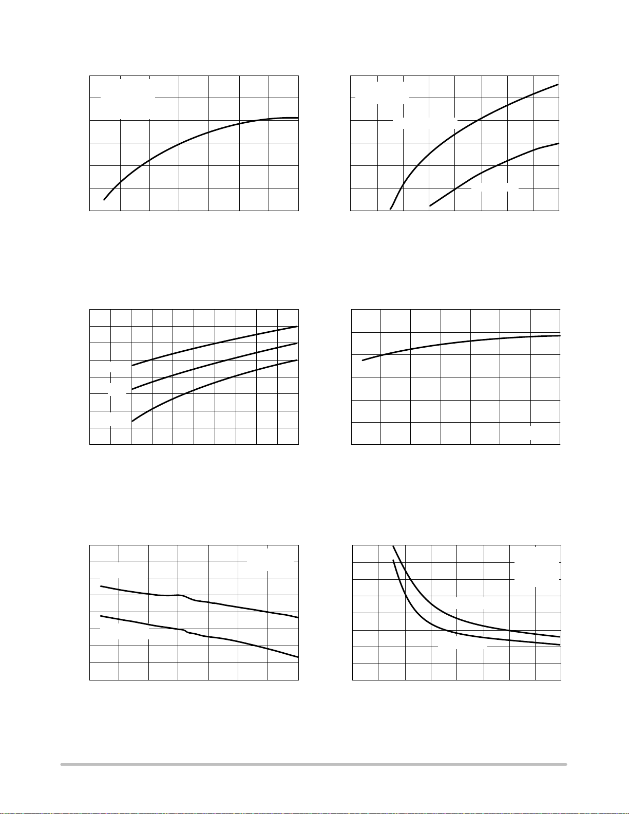
0.4
0.2
Vin = 20 V
I
= 200 mA
Load
Normalized at
TJ = 25°C
LM2575
TYPICAL PERFORMANCE CHARACTERISTICS (Circuit of Figure 14)
1.00.6
I
= 200 mA
Load
TJ = 25°C
0.8
0.6
3.3 V, 5.0 V and Adj
0
−0.2
, OUTPUT VOLTAGE CHANGE (%)
−0.4
out
V
−0.6
−50
Figure 2. Normalized Output Voltage
1.2
1.1
1.0
, SATURATION VOLTAGE (V)
V
sat
0.9
0.8
0.7
0.6
0.5
0.4
−40°C
25°C
125°C
0
TJ, JUNCTION TEMPERATURE (°C)
SWITCH CURRENT (A)
0.8 0.9 1.0
0.4
0.2
, OUTPUT VOLTAGE CHANGE (%)
0
out
V
−0.2
0
5.0−25 100 201525 257550 3530 40100 125
3.0
2.5
2.0
1.5
1.0
, OUTPUT CURRENT (A)
O
I
0.5
0
−50
−250.1 00.2 250.3 500.4 750.5 1000.6 1250.7
12 V and 15 V
Vin, INPUT VOLTAGE (V)
Figure 3. Line Regulation
Vin = 25 V
TJ, JUNCTION TEMPERATURE (°C)
INPUT−OUTPUT DIFFERENTIAL (V)
2.0
1.8
1.6
1.4
1.2
1.0
0.8
0.6
0.4
−50
Figure 4. Switch Saturation Voltage Figure 5. Current Limit
, QUIESCENT CURRENT (mA)
Q
I
8.0
6.0
4.0
20
18
16
14
I
Load
= 1.0 A
12
10
I
= 200 mA
Load
0
5.0−25 100 1525 2050 2575 30100 35125
Vin, INPUT VOLTAGE (V)
I
Load
I
Load
= 1.0 A
= 200 mA
TJ, JUNCTION TEMPERATURE (°C)
DV
R
ind
= 5%
out
= 0.2 W
Figure 6. Dropout Voltage Figure 7. Quiescent Current
http://onsemi.com
5
V
= 5.0 V
out
Measured at
Ground Pin
TJ = 25°C
40
Page 6
LM2575
, STANDBY QUIESCENT CURRENT ( A)μ
I
stby
−2.0
120
100
2.0
80
60
40
20
0
0
0
TJ = 25°C
5.0
10
15
20
25
Vin, INPUT VOLTAGE (V)
Figure 8. Standby Quiescent Current
Vin = 12 V
Normalized at 25°C
120
Vin = 12 V
V
= 5.0 V
ON/OFF
100
80
60
40
20
, STANDBY QUIESCENT CURRENT ( A)μ
0
stby
I
−50
30
4035
−25
0
25
50
75
100
125
TJ, JUNCTION TEMPERATURE (°C)
Figure 9. Standby Quiescent Current
40
Adjustable
Version Only
20
−4.0
−6.0
NORMALIZED FREQUENCY (%)
−8.0
−10
−50
OUTPUT
VOLTAGE
(PIN 2)
OUTPUT
CURRENT
(PIN 2)
INDUCTOR
CURRENT
OUTPUT
RIPPLE
VOLTAGE
0
−20
, FEEDBACK PIN CURRENT (nA)
FB
I
−40
−50
−25
0
25
TJ, JUNCTION TEMPERATURE (°C)
50
75
100
125
−25
0
25
TJ, JUNCTION TEMPERATURE (°C)
Figure 10. Oscillator Frequency Figure 11. Feedback Pin Current
10 V
1.0 A
0.5 A
20 mV
/DIV
0
5.0 ms/DIV
100
00
CHANGE (mV)
, OUTPUT VOLTAGE
−1001.0 A
out
V
1.0
0.5
0
, LOAD CURRENT (A)
Load
I
100 ms/DIV
Figure 12. Switching Waveforms Figure 13. Load Transient Response
50
75
100
125
http://onsemi.com
6
Page 7
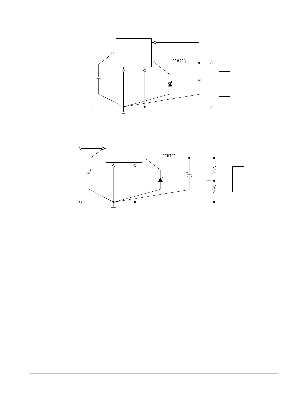
Unregulated
5.0 Output Voltage Versions
DC Input
8.0 V − 40 V
Unregulated
DC Input
8.0 V − 40 V
LM2575
Feedback
53ON/OFFGND
Feedback
4
Output
2
4
Output
2
L1
330 mH
D1
1N5819
L1
330 mH
D1
1N5819
C
out
330 mF
/16 V
C
out
330 mF
/16 V
V
out
Regulated
Output
Load
R2
R1
V
out
Regulated
Output
Load
V
in
LM2575−5
+
V
in
−
1
C
in
100 mF/50 V
Adjustable Output Voltage Versions
V
in
LM2575
Adjustable
+
1
C
in
100 mF/50 V
53ON/OFFGND
−
V
+ V
out
R2 + R1ǒ
Where V
between 1.0 kW and 5.0 kW
Figure 14. Typical Test Circuit
PCB LAYOUT GUIDELINES
As in any switching regulator, the layout of the printed
circuit board is very important. Rapidly switching currents
associated with wiring inductance, stray capacitance and
parasitic inductance of the printed circuit board traces can
generate voltage transients which can generate
electromagnetic interferences (EMI) and affect the desired
operation. As indicated in the Figure 14, to minimize
inductance and ground loops, the length of the leads
indicated by heavy lines should be kept as short as possible.
For best results, single−point grounding (as indicated) or
ground plane construction should be used.
ref
ref
R1
V
out
–1Ǔ
V
ref
= 1.23 V, R1
R2
ǒ
Ǔ
1 )
On the other hand, the PCB area connected to the Pin 2
(emitter of the internal switch) of the LM2575 should be
kept to a minimum in order to minimize coupling to sensitive
circuitry.
Another sensitive part of the circuit is the feedback. It is
important to keep the sensitive feedback wiring short. To
assure this, physically locate the programming resistors near
to the regulator, when using the adjustable version of the
LM2575 regulator.
http://onsemi.com
7
Page 8
LM2575
PIN FUNCTION DESCRIPTION
Pin Symbol Description (Refer to Figure 1)
1 V
2 Output This is the emitter of the internal switch. The saturation voltage V
3 GND Circuit ground pin. See the information about the printed circuit board layout.
4 Feedback This pin senses regulated output voltage to complete the feedback loop. The signal is divided by the
5 ON/OFF It allows the switching regulator circuit to be shut down using logic level signals, thus dropping the total
in
This pin is the positive input supply for the LM2575 step−down switching regulator. In order to minimize
voltage transients and to supply the switching currents needed by the regulator, a suitable input bypass
capacitor must be present (Cin in Figure 1).
of this output switch is typically 1.0 V.
It should be kept in mind that the PCB area connected to this pin should be kept to a minimum in order to
minimize coupling to sensitive circuitry.
internal resistor divider network R2, R1 and applied to the non−inverting input of the internal error amplifier.
In the Adjustable version of the LM2575 switching regulator this pin is the direct input of the error amplifier
and the resistor network R2, R1 is connected externally to allow programming of the output voltage.
input supply current to approximately 80 mA. The input threshold voltage is typically 1.4 V. Applying a
voltage above this value (up to +Vin) shuts the regulator off. If the voltage applied to this pin is lower than
1.4 V or if this pin is connected to ground, the regulator will be in the “on” condition.
sat
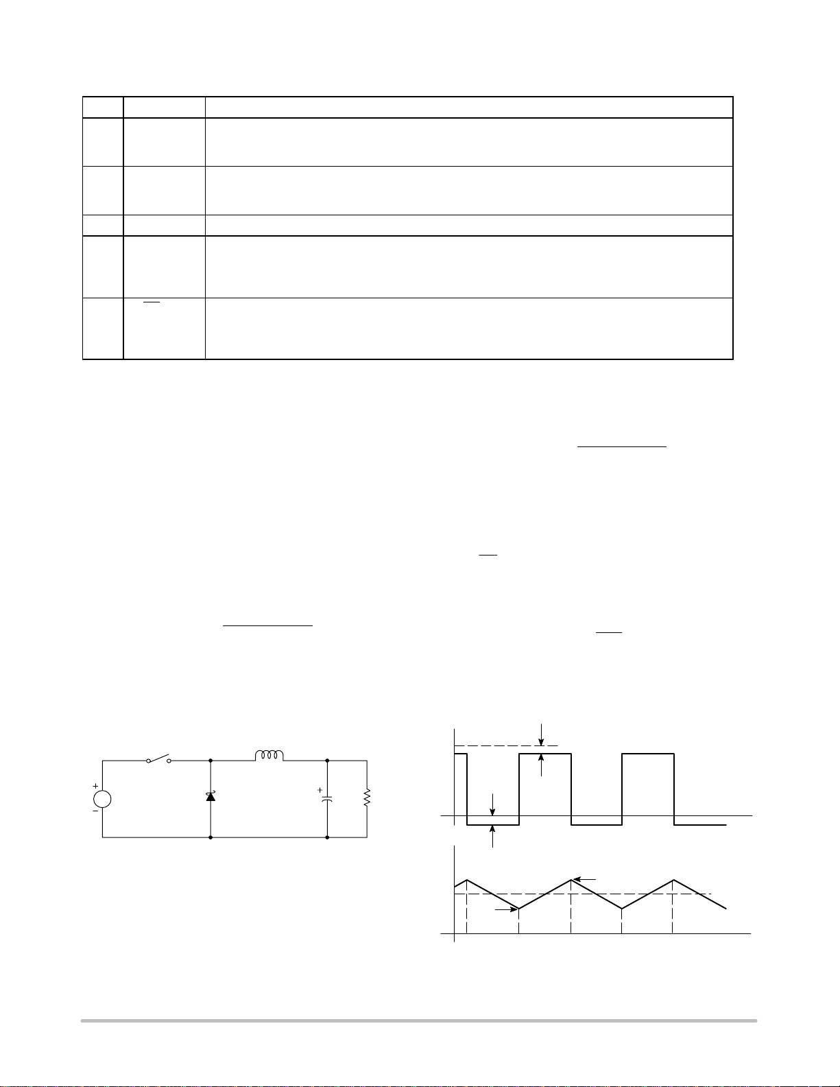
DESIGN PROCEDURE
Buck Converter Basics
The LM2575 is a “Buck” or Step−Down Converter which
is the most elementary forward−mode converter. Its basic
schematic can be seen in Figure 15.
The operation of this regulator topology has two distinct
time periods. The first one occurs when the series switch is
on, the input voltage is connected to the input of the inductor.
The output of the inductor is the output voltage, and the
rectifier (or catch diode) is reverse biased. During this
period, since there is a constant voltage source connected
across the inductor, the inductor current begins to linearly
ramp upwards, as described by the following equation:
I
L(on)
+
ǒ
Vin–V
L
out
Ǔ
t
on
During this “on” period, energy is stored within the core
material in the form of magnetic flux. If the inductor is
properly designed, there is sufficient energy stored to carry
the requirements of the load during the “off” period.
Power
Switch
V
in
D1
L
C
out
V
out
R
Load
The inductor current during this time is:
I
L(off)
+
ǒ
V
out
–V
L
Ǔ
t
D
off
This period ends when the power switch is once again
turned on. Regulation of the converter is accomplished by
varying the duty cycle of the power switch. It is possible to
describe the duty cycle as follows:
t
on
d +
, where T is the period of switching.
T
For the buck converter with ideal components, the duty
cycle can also be described as:
V
out
d +
V
in
Figure 16 shows the buck converter idealized waveforms
of the catch diode voltage and the inductor current.
V
on(SW)
Power
Switch
Off
Diode VoltageInductor Current
Power
Switch
On
Power
Switch
Off
Power
Switch
On
Time
Figure 15. Basic Buck Converter
The next period is the “off” period of the power switch.
When the power switch turns off, the voltage across the
inductor reverses its polarity and is clamped at one diode
voltage drop below ground by catch dioded. Current now
flows through the catch diode thus maintaining the load
current loop. This removes the stored energy from the
inductor.
http://onsemi.com
VD(FWD)
I
I
min
Diode Diode
Power
Switch
pk
Power
Switch
I
Load
(AV)
Time
Figure 16. Buck Converter Idealized Waveforms
8
Page 9
LM2575
Procedure (Fixed Output Voltage Version) In order to simplify the switching regulator design, a step−by−step design
procedure and example is provided.
Procedure Example
Given Parameters:
V
= Regulated Output Voltage (3.3 V, 5.0 V, 12 V or 15 V)
out
V
= Maximum DC Input Voltage
in(max)
I
Load(max)
= Maximum Load Current
1. Controller IC Selection
According to the required input voltage, output voltage and
current, select the appropriate type of the controller IC output
voltage version.
2. Input Capacitor Selection (Cin)
To prevent large voltage transients from appearing at the input
and for stable operation of the converter, an aluminium or
tantalum electrolytic bypass capacitor is needed between the
input pin +Vin and ground pin GND. This capacitor should be
located close to the IC using short leads. This capacitor should
have a low ESR (Equivalent Series Resistance) value.
3. Catch Diode Selection (D1)
A.Since the diode maximum peak current exceeds the
regulator maximum load current the catch diode current
rating must be at least 1.2 times greater than the maximum
load current. For a robust design the diode should have a
current rating equal to the maximum current limit of the
LM2575 to be able to withstand a continuous output short
B.The reverse voltage rating of the diode should be at least
1.25 times the maximum input voltage.
4. Inductor Selection (L1)
A.According to the required working conditions, select the
correct inductor value using the selection guide from
Figures 17 to 21.
B.From the appropriate inductor selection guide, identify the
inductance region intersected by the Maximum Input
Voltage line and the Maximum Load Current line. Each
region is identified by an inductance value and an inductor
code.
C.Select an appropriate inductor from the several different
manufacturers part numbers listed in Table 1 or Table 2.
When using Table 2 for selecting the right inductor the
designer must realize that the inductor current rating must
be higher than the maximum peak current flowing through
the inductor. This maximum peak current can be calculated
as follows:
I
p(max)
+ I
Load(max)
)
ǒ
Vin–V
2L
out
Ǔ
t
on
where ton is the “on” time of the power switch and
V
out
t
+
on
V
1
x
f
osc
in
For additional information about the inductor, see the
inductor section in the “External Components” section of
this data sheet.
Given Parameters:
V
= 5.0 V
out
V
= 20 V
in(max)
I
Load(max)
= 0.8 A
1. Controller IC Selection
According to the required input voltage, output voltage,
current polarity and current value, use the LM2575−5
controller IC
2. Input Capacitor Selection (Cin)
A 47 mF, 25 V aluminium electrolytic capacitor located near
to the input and ground pins provides sufficient bypassing.
3. Catch Diode Selection (D1)
A.For this example the current rating of the diode is 1.0 A.
B.Use a 30 V 1N5818 Schottky diode, or any of the
suggested fast recovery diodes shown in the Table 4.
4. Inductor Selection (L1)
A.Use the inductor selection guide shown in Figures 17
to 21.
B.From the selection guide, the inductance area intersected
by the 20 V line and 0.8 A line is L330.
C.Inductor value required is 330 mH. From the Table 1 or
Table 2, choose an inductor from any of the listed
manufacturers.
http://onsemi.com
9
Page 10

LM2575
Procedure (Fixed Output Voltage Version) (continued)In order to simplify the switching regulator design, a step−by−step design
procedure and example is provided.
Procedure Example
5. Output Capacitor Selection (C
A.Since the LM2575 is a forward−mode switching regulator
with voltage mode control, its open loop 2−pole−2−zero
frequency characteristic has the dominant pole−pair
determined by the output capacitor and inductor values. For
stable operation and an acceptable ripple voltage,
(approximately 1% of the output voltage) a value between
100 mF and 470 mF is recommended.
B.Due to the fact that the higher voltage electrolytic capacitors
generally have lower ESR (Equivalent Series Resistance)
numbers, the output capacitor’s voltage rating should be at
least 1.5 times greater than the output voltage. For a 5.0 V
regulator, a rating at least 8V is appropriate, and a 10 V or
16 V rating is recommended.
Procedure (Adjustable Output Version: LM2575−Adj)
Procedure Example
Given Parameters:
V
= Regulated Output Voltage
out
V
= Maximum DC Input Voltage
in(max)
I
Load(max)
1. Programming Output Voltage
To select the right programming resistor R1 and R2 value (see
Figure 14) use the following formula:
Resistor R1 can be between 1.0 k and 5.0 kW. (For best
temperature coefficient and stability with time, use 1% metal
film resistors).
= Maximum Load Current
R2
+ V
ǒ
1 )
ref
R2 + R1
R1
V
out
Ǔ
V
ǒ
V
)
out
where V
out
–1
ref
ref
Ǔ
= 1.23 V
5. Output Capacitor Selection (C
A.C
= 100 mF to 470 mF standard aluminium electrolytic.
out
B.Capacitor voltage rating = 16 V.
Given Parameters:
V
= 8.0 V
out
V
= 12 V
in(max)
I
Load(max)
1. Programming Output Voltage (selecting R1 and R2)
Select R1 and R2:
= 1.0 A
V
out
* 1Ǔ+ 1.8 k
V
ref
R2
R1
V
+ 1.23ǒ1 )
out
R2 + R1
R2 = 9.91 kW, choose a 9.88 k metal film resistor.
ǒ
)
out
Ǔ
Select R1 = 1.8 kW
8.0 V
ǒ
1.23 V
* 1
Ǔ
2. Input Capacitor Selection (Cin)
To prevent large voltage transients from appearing at the input
and for stable operation of the converter, an aluminium or
tantalum electrolytic bypass capacitor is needed between the
input pin +V
located close to the IC using short leads. This capacitor should
have a low ESR (Equivalent Series Resistance) value.
For additional information see input capacitor section in the
“External Components” section of this data sheet.
3. Catch Diode Selection (D1)
A.Since the diode maximum peak current exceeds the
regulator maximum load current the catch diode current
rating must be at least 1.2 times greater than the maximum
load current. For a robust design, the diode should have a
current rating equal to the maximum current limit of the
LM2575 to be able to withstand a continuous output short.
B.The reverse voltage rating of the diode should be at least
1.25 times the maximum input voltage.
and ground pin GND This capacitor should be
in
2. Input Capacitor Selection (Cin)
A 100 mF aluminium electrolytic capacitor located near the
input and ground pin provides sufficient bypassing.
3. Catch Diode Selection (D1)
A.For this example, a 3.0 A current rating is adequate.
B.Use a 20 V 1N5820 or MBR320 Schottky diode or any
suggested fast recovery diode in the Table 4.
http://onsemi.com
10
Page 11

LM2575
Procedure (Adjustable Output Version: LM2575−Adj) (continued)
Procedure Example
4. Inductor Selection (L1)
A.Use the following formula to calculate the inductor Volt x
microsecond [V x ms] constant:
V
out
ExT+ǒVin–V
B.Match the calculated E x T value with the corresponding
number on the vertical axis of the Inductor Value Selection
Guide shown in Figure 21. This E x T constant is a measure
of the energy handling capability of an inductor and is
dependent upon the type of core, the core area, the number
of turns, and the duty cycle.
C.Next step is to identify the inductance region intersected by
the E x T value and the maximum load current value on the
horizontal axis shown in Figure 21.
D.From the inductor code, identify the inductor value. Then
select an appropriate inductor from the Table 1 or Table 2.
The inductor chosen must be rated for a switching
frequency of 52 kHz and for a current rating of 1.15 x I
The inductor current rating can also be determined by
calculating the inductor peak current:
I
+ I
p(max)
where ton is the “on” time of the power switch and
For additional information about the inductor, see the
inductor section in the “External Components” section of
this data sheet.
5. Output Capacitor Selection (C
A.Since the LM2575 is a forward−mode switching regulator
with voltage mode control, its open loop 2−pole−2−zero
frequency characteristic has the dominant pole−pair
determined by the output capacitor and inductor values.
For stable operation, the capacitor must satisfy the
following requirement:
C
w 7.785
out
B.Capacitor values between 10 mF and 2000 mF will satisfy
the loop requirements for stable operation. To achieve an
acceptable output ripple voltage and transient response, the
output capacitor may need to be several times larger than
the above formula yields.
C.Due to the fact that the higher voltage electrolytic capacitors
generally have lower ESR (Equivalent Series Resistance)
numbers, the output capacitor’s voltage rating should be at
least 1.5 times greater than the output voltage. For a 5.0 V
regulator, a rating of at least 8V is appropriate, and a 10 V
or 16 V rating is recommended.
Ǔ
out
V
Load(max)
V
t
+
on
V
V
out
on
out
V
in
in(max)
10
x
F[Hz]
ǒ
Vin–V
)
x
f
osc
)
out
xL[μH]
1
6
2L
[μF]
[V x ms]
Ǔ
t
out
on
Ioad
4. Inductor Selection (L1)
A.Calculate E x T [V x ms] constant:
B.E x T = 51 [V x ms]
C.I
D.Proper inductor value = 220 mH
.
5. Output Capacitor Selection (C
A.
8.0
ExT+(12–8.0)x
Load(max)
Inductance Region = L220
Choose the inductor from the Table 1 or Table 2.
To achieve an acceptable ripple voltage, select
C
= 1.0 A
C
w 7.785
out
= 100 mF electrolytic capacitor.
out
12
8.220
x
12
out
+ 53 μF
1000
+ 51 [V x ms]
52
)
http://onsemi.com
11
Page 12
LM2575
O
G
INDUCTOR VALUE SELECTION GUIDE
, MAXIMUM INPUT VOLTAGE (V)
V
, MAXIMUM INPUT VOLTAGE (V)
V
60
H1500H1000
40
25
20
15
12
10
9.0
8.0
in
7.05.0
0.2
H1000
0.30.3
IL, MAXIMUM LOAD CURRENT (A)
L680
L470
0.40.4
L330
L220
L150
0.50.5
0.60.6
0.7
0.80.8
0.9
1.01.0
Figure 18. LM2575−5.0
60
40
35
30
25
22
20
19
18
in
17
0.2
H2200
H1500
L680
0.3
IL, MAXIMUM LOAD CURRENT (A)
0.4
H1000
L470
0.5
0.6
L330
H680
0.7
0.8
H470
L220
0.9
1.0
60
20
E (V)
15
10
LTA
8.0
7.0
6.0
, MAXIMUM INPUT V
in
V
0.2
L680
L470
L330
L220
L150
L100
IL, MAXIMUM LOAD CURRENT (A)
Figure 17. LM2575−3.3
60
H2200
0.3 0.4 0.5 0.6 0.7 0.8 0.9 1.0
IL, MAXIMUM LOAD CURRENT (A)
L680
H1500
L470
H1000
H680
L330
H470
L220
, MAXIMUM INPUT VOLTAGE (V)
V
40
30
25
20
18
17
16
15
in
14
0.2
Figure 19. LM2575−12 Figure 20. LM2575−15
200
150
125
100
ET, VOLTAGE TIME (V s)μ
H2200
80
70
60
50
40
30
20
0.2
H1500
H1000
H680
L680
L470
L330
L220
0.3 0.4 0.5 0.6 0.7 0.8 0.9 1.0
IL, MAXIMUM LOAD CURRENT (A)
Figure 21. LM2575−Adj
NOTE: This Inductor Value Selection Guide is applicable for continuous mode only.
H470
L150
L100
http://onsemi.com
12
Page 13

Inductor
Code
L100
L150
L220
L330
L470
L680
H150
H220
H330
H470
H680
H1000
H1500
H2200
Inductor
Value
100 mH
150 mH
220 mH
330 mH
470 mH
680 mH
150 mH
220 mH
330 mH
470 mH
680 mH
1000 mH
1500 mH
2200 mH
LM2575
Table 1. Inductor Selection Guide
Pulse Eng Renco AIE Tech 39
PE−92108 RL2444 415−0930 77 308 BV
PE−53113 RL1954 415−0953 77 358 BV
PE−52626 RL1953 415−0922 77 408 BV
PE−52627 RL1952 415−0926 77 458 BV
PE−53114 RL1951 415−0927 −
PE−52629 RL1950 415−0928 77 508 BV
PE−53115 RL2445 415−0936 77 368 BV
PE−53116 RL2446 430−0636 77 410 BV
PE−53117 RL2447 430−0635 77 460 BV
PE−53118 RL1961 430−0634 −
PE−53119 RL1960 415−0935 77 510 BV
PE−53120 RL1959 415−0934 77 558 BV
PE−53121 RL1958 415−0933 −
PE−53122 RL2448 415−0945 77 610 BV
Table 2. Inductor Selection Guide
Inductance Current Schott Renco Pulse Engineering Coilcraft
(mH)
68
100
150
220
330
NOTE: Table 1 and Table 2 of this Indicator Selection Guide shows some examples of different manufacturer products suitable for design
with the LM2575.
(A) THT SMT THT SMT THT SMT SMT
0.32 67143940 67144310 RL−1284−68−43 RL1500−68 PE−53804 PE−53804−S DO1608−68
0.58 67143990 67144360 RL−5470−6 RL1500−68 PE−53812 PE−53812−S DO3308−683
0.99 67144070 67144450 RL−5471−5 RL1500−68 PE−53821 PE−53821−S DO3316−683
1.78 67144140 67144520 RL−5471−5 − PE−53830 PE−53830−S DO5022P−683
0.48 67143980 67144350 RL−5470−5 RL1500−100 PE−53811 PE−53811−S DO3308−104
0.82 67144060 67144440 RL−5471−4 RL1500−100 PE−53820 PE−53820−S DO3316−104
1.47 67144130 67144510 RL−5471−4 − PE−53829 PE−53829−S DO5022P−104
0.39 − 67144340 RL−5470−4 RL1500−150 PE−53810 PE−53810−S DO3308−154
0.66 67144050 67144430 RL−5471−3 RL1500−150 PE−53819 PE−53819−S DO3316−154
1.20 67144120 67144500 RL−5471−3 − PE−53828 PE−53828−S DO5022P−154
0.32 67143960 67144330 RL−5470−3 RL1500−220 PE−53809 PE−53809−S DO3308−224
0.55 67144040 67144420 RL−5471−2 RL1500−220 PE−53818 PE−53818−S DO3316−224
1.00 67144110 67144490 RL−5471−2 − PE−53827 PE−53827−S DO5022P−224
0.42 67144030 67144410 RL−5471−1 RL1500−330 PE−53817 PE−53817−S DO3316−334
0.80 67144100 67144480 RL−5471−1 − PE−53826 PE−53826−S DO5022P−334
http://onsemi.com
13
Page 14
LM2575
Table 3. Example of Several Inductor Manufacturers Phone/Fax Numbers
Pulse Engineering Inc.
Phone
Fax
+ 1−619−674−8100
+ 1−619−674−8262
Pulse Engineering Inc. Europe
Renco Electronics Inc.
AIE Magnetics
Coilcraft Inc.
Coilcraft Inc., Europe
Tech 39
Schott Corp.
Phone
Fax
Phone
Fax
Phone
Fax
Phone
Fax
Phone
Fax
Phone
Fax
Phone
Fax
+ 353 93 24 107
+ 353 93 24 459
+ 1−516−645−5828
+ 1−516−586−5562
+ 1−813−347−2181
+ 1−708−322−2645
+ 1−708−639−1469
+ 44 1236 730 595
+ 44 1236 730 627
+ 33 8425 2626
+ 33 8425 2610
+ 1−612−475−1173
+ 1−612−475−1786
Table 4. Diode Selection Guide gives an overview about both surface−mount and through−hole diodes for an
effective design. Device listed in bold are available from ON Semiconductor.
Schottky Ultra−Fast Recovery
1.0 A 3.0 A 1.0 A 3.0 A
V
R
20 V SK12 1N5817
30 V MBRS130LT3
40 V MBRS140T3
50 V MBRS150
SMT THT SMT THT SMT THT SMT THT
SK13
SK14
10BQ040
10MQ040
10BQ050
SR102
1N5818
SR103
11DQ03
1N5819
SR104
11DQ04
MBR150
SR105
11DQ05
SK32
MBRD320
SK33
MBRD330
MBRS340T3
MBRD340
30WQ04
SK34
MBRD350
SK35
30WQ05
1N5820
MBR320
SR302
1N5821
MBR330
SR303
31DQ03
1N5822
MBR340
SR304
31DQ04
MBR350
SR305
11DQ05
MURS120T3
10BF10 MURD320 MUR320
MUR120
11DF1
HER102
MURS320T3
31DF1
HER302
30WF10
MUR420
http://onsemi.com
14
Page 15

LM2575
V
a
out
r.
EXTERNAL COMPONENTS
Input Capacitor (Cin)
The Input Capacitor Should Have a Low ESR
For stable operation of the switch mode converter a low
ESR (Equivalent Series Resistance) aluminium or solid
tantalum bypass capacitor is needed between the input pin
and the ground pin to prevent large voltage transients from
appearing at the input. It must be located near the regulator
and use short leads. With most electrolytic capacitors, the
capacitance value decreases and the ESR increases with
lower temperatures. For reliable operation in temperatures
below −25°C larger values of the input capacitor may be
needed. Also paralleling a ceramic or solid tantalum
capacitor will increase the regulator stability at cold
temperatures.
RMS Current Rating of C
in
The important parameter of the input capacitor is the RMS
current rating. Capacitors that are physically large and have
large surface area will typically have higher RMS current
ratings. For a given capacitor value, a higher voltage
electrolytic capacitor will be physically larger than a lower
voltage capacitor, and thus be able to dissipate more heat to
the surrounding air, and therefore will have a higher RMS
current rating. The consequence of operating an electrolytic
capacitor above the RMS current rating is a shortened
operating life. In order to assure maximum capacitor
operating lifetime, the capacitor’s RMS ripple current rating
should be:
I
> 1.2 x d x I
rms
Load
where d is the duty cycle, for a buck regulator
t
on
out
+
T
V
in
for a buck*boost regulato
t
nd d +
Output Capacitor (C
on
T
+
|V
d +
|V
out
| ) V
out
|
)
For low output ripple voltage and good stability, low ESR
output capacitors are recommended. An output capacitor
has two main functions: it filters the output and provides
regulator loop stability. The ESR of the output capacitor and
the peak−to−peak value of the inductor ripple current are the
main factors contributing to the output ripple voltage value.
Standard aluminium electrolytics could be adequate for
some applications but for quality design low ESR types are
recommended.
An aluminium electrolytic capacitor’s ESR value is
related to many factors such as the capacitance value, the
voltage rating, the physical size and the type of construction.
In most cases, the higher voltage electrolytic capacitors have
lower ESR value. Often capacitors with much higher
voltage ratings may be needed to provide low ESR values
that are required for low output ripple voltage.
The Output Capacitor Requires an ESR Value
That Has an Upper and Lower Limit
As mentioned above, a low ESR value is needed for low
output ripple voltage, typically 1% to 2% of the output
voltage. But if the selected capacitor’s ESR is extremely low
(below 0.05 W), there is a possibility of an unstable feedback
loop, resulting in oscillation at the output. This situation can
occur when a tantalum capacitor, that can have a very low
ESR, is used as the only output capacitor.
At Low Temperatures, Put in Parallel Aluminium
Electrolytic Capacitors with Tantalum Capacitors
Electrolytic capacitors are not recommended for
temperatures below −25°C. The ESR rises dramatically at
cold temperatures and typically rises 3 times at −25°C and
as much as 10 times at −40°C. Solid tantalum capacitors
have much better ESR spec at cold temperatures and are
recommended for temperatures below −25°C. They can be
also used in parallel with aluminium electrolytics. The value
of the tantalum capacitor should be about 10% or 20% of the
total capacitance. The output capacitor should have at least
50% higher RMS ripple current rating at 52 kHz than the
peak−to−peak inductor ripple current.
Catch Diode
Locate the Catch Diode Close to the LM2575
The LM2575 is a step−down buck converter; it requires a
fast diode to provide a return path for the inductor current
when the switch turns off. This diode must be located close
to the LM2575 using short leads and short printed circuit
traces to avoid EMI problems.
Use a Schottky or a Soft Switching
Ultra−Fast Recovery Diode
Since the rectifier diodes are very significant source of
losses within switching power supplies, choosing the
rectifier that best fits into the converter design is an
important process. Schottky diodes provide the best
performance because of their fast switching speed and low
forward voltage drop.
They provide the best efficiency especially in low output
voltage applications (5.0 V and lower). Another choice
could be Fast−Recovery, or Ultra−Fast Recovery diodes. It
has to be noted, that some types of these diodes with an
abrupt turnoff characteristic may cause instability or EMI
troubles.
A fast−recovery diode with soft recovery characteristics
can better fulfill a quality, low noise design requirements.
Table 4 provides a list of suitable diodes for the LM2575
regulator. Standard 50/60 Hz rectifier diodes such as the
1N4001 series or 1N5400 series are NOT suitable.
Inductor
The magnetic components are the cornerstone of all
switching power supply designs. The style of the core and
the winding technique used in the magnetic component’s
design has a great influence on the reliability of the overall
power supply.
Using an improper or poorly designed inductor can cause
high voltage spikes generated by the rate of transitions in
current within the switching power supply, and the
possibility of core saturation can arise during an abnormal
operational mode. Voltage spikes can cause the
semiconductors to enter avalanche breakdown and the part
can instantly fail if enough energy is applied. It can also
http://onsemi.com
15
Page 16

LM2575
cause significant RFI (Radio Frequency Interference) and
EMI (Electro−Magnetic Interference) problems.
Continuous and Discontinuous Mode of Operation
The LM2575 step−down converter can operate in both the
continuous and the discontinuous modes of operation. The
regulator works in the continuous mode when loads are
relatively heavy, the current flows through the inductor
continuously and never falls to zero. Under light load
conditions, the circuit will be forced to the discontinuous
mode when inductor current falls to zero for certain period
of time (see Figure 22 and Figure 23). Each mode has
distinctively different operating characteristics, which can
affect the regulator performance and requirements. In many
cases the preferred mode of operation is the continuous
mode. It offers greater output power, lower peak currents in
the switch, inductor and diode, and can have a lower output
ripple voltage. On the other hand it does require larger
inductor values to keep the inductor current flowing
continuously, especially at low output load currents and/or
high input voltages.
To simplify the inductor selection process, an inductor
selection guide for the LM2575 regulator was added to this
data sheet (Figures 17 through 21). This guide assumes that
the regulator is operating in the continuous mode, and
selects an inductor that will allow a peak−to−peak inductor
ripple current to be a certain percentage of the maximum
design load current. This percentage is allowed to change as
different design load currents are selected. For light loads
(less than approximately 200 mA) it may be desirable to
operate the regulator in the discontinuous mode, because the
inductor value and size can be kept relatively low.
Consequently, the percentage of inductor peak−to−peak
current increases. This discontinuous mode of operation is
perfectly acceptable for this type of switching converter.
Any buck regulator will be forced to enter discontinuous
mode if the load current is light enough.
1.0
the physical volume the inductor must fit within, and the
amount of EMI (Electro−Magnetic Interference) shielding
that the core must provide. The inductor selection guide
covers dif ferent styles o f inductors, such as pot core, E−core,
toroid and bobbin core, as well as different core materials
such as ferrites and powdered iron from different
manufacturers.
For high quality design regulators the toroid core seems to
be the best choice. Since the magnetic flux is completely
contained within the core, it generates less EMI, reducing
noise problems in sensitive circuits. The least expensive is
the bobbin core type, which consists of wire wound on a
ferrite rod core. This type of inductor generates more EMI
due to the fact that its core is open, and the magnetic flux is
not completely contained within the core.
When multiple switching regulators are located on the
same printed circuit board, open core magnetics can cause
interference between two or more of the regulator circuits,
especially at high currents due to mutual coupling. A toroid,
pot core or E−core (closed magnetic structure) should be
used in such applications.
Do Not Operate an Inductor Beyond its
Maximum Rated Current
Exceeding an inductor’s maximum current rating may
cause the inductor to overheat because of the copper wire
losses, or the core may saturate. Core saturation occurs when
the flux density is too high and consequently the cross
sectional area of the core can no longer support additional
lines of magnetic flux.
This causes the permeability of the core to drop, the
inductance value decreases rapidly and the inductor begins
to look mainly resistive. It has only the dc resistance of the
winding. This can cause the switch current to rise very
rapidly and force the LM2575 internal switch into
cycle−by−cycle current limit, thus reducing the dc output
load current. This can also result in overheating of the
inductor and/or the LM2575. Different inductor types have
different saturation characteristics, and this should be kept
in mind when selecting an inductor.
0
CURRENT (A)
POWER SWITCH
1.0
INDUCTOR
CURRENT (A)
0
HORIZONTAL TIME BASE: 5.0 ms/DIV
Figure 22. Continuous Mode Switching
Current Waveforms
Selecting the Right Inductor Style
Some important considerations when selecting a core type
are core material, cost, the output power of the power supply,
http://onsemi.com
16
0.1
0
CURRENT (A)
POWER SWITCH
0.1
0
INDUCTOR
CURRENT (A)
Figure 23. Discontinuous Mode Switching
HORIZONTAL TIME BASE: 5.0 ms/DIV
Current Waveforms
Page 17

LM2575
GENERAL RECOMMENDATIONS
Output Voltage Ripple and Transients
Source of the Output Ripple
Since the LM2575 is a switch mode power supply
regulator, its output voltage, if left unfiltered, will contain a
sawtooth ripple voltage at the switching frequency. The
output ripple voltage value ranges from 0.5% to 3% of the
output voltage. It is caused mainly by the inductor sawtooth
ripple current multiplied by the ESR of the output capacitor .
Short Voltage Spikes and How to Reduce Them
The regulator output voltage may also contain short
voltage spikes at the peaks of the sawtooth waveform (see
Figure 24). These voltage spikes are present because of the
fast switching action of the output switch, and the parasitic
inductance of the output filter capacitor. There are some
other important factors such as wiring inductance, stray
capacitance, as well as the scope probe used to evaluate these
transients, all these contribute to the amplitude of these
spikes. To minimize these voltage spikes, low inductance
capacitors should be used, and their lead lengths must be
kept short. The importance of quality printed circuit board
layout design should also be highlighted.
Voltage spikes caused by switching action of the output
switch and the parasitic inductance of the output capacitor
UNFILTERED
OUTPUT
VOLTAGE
VERTICAL
RESOLUTION:
20 mV/DIV
FILTERED
OUTPUT
VOLTAGE
HORIZONTAL TIME BASE: 10 ms/DIV
Figure 24. Output Ripple Voltage Waveforms
Minimizing the Output Ripple
In order to minimize the output ripple voltage it is possible
to enlarge the inductance value of the inductor L1 and/or to
use a lar ger value output capacitor. There is also another way
to smooth the output by means of an additional LC filter
(20 mH, 100 mF), that can be added to the output (see
Figure 33) to further reduce the amount of output ripple and
transients. With such a filter it is possible to reduce the
output ripple voltage transients 10 times or more. Figure 24
shows the difference between filtered and unfiltered output
waveforms of the regulator shown in Figure 33.
The upper waveform is from the normal unfiltered output
of the converter, while the lower waveform shows the output
ripple voltage filtered by an additional LC filter.
Heatsinking and Thermal Considerations
The Through−Hole Package TO−220
The LM2575 is available in two packages, a 5−pin
TO−220(T, TV) and a 5−pin surface mount D2PAK(D2T).
There are many applications that require no heatsink to keep
the LM2575 junction temperature within the allowed
operating range. The TO−220 package can be used without
a heatsink for ambient temperatures up to approximately
50°C (depending on the output voltage and load current).
Higher ambient temperatures require some heatsinking,
either to the printed circuit (PC) board or an external
heatsink.
The Surface Mount Package D2PAK and its
Heatsinking
The other type of package, the surface mount D2PAK, is
designed to be soldered to the copper on the PC board. The
copper and the board are the heatsink for this package and
the other heat producing components, such as the catch
diode and inductor. The PC board copper area that the
package is soldered to should be at least 0.4 in2 (or 100 mm2)
and ideally should have 2 or more square inches (1300 mm2)
of 0.0028 inch copper. Additional increasing of copper area
beyond approximately 3.0 in2 (2000 mm2) will not improve
heat dissipation significantly. If further thermal
improvements are needed, double sided or multilayer PC
boards with large copper areas should be considered.
Thermal Analysis and Design
The following procedure must be performed to determine
whether or not a heatsink will be required. First determine:
1. P
maximum regulator power dissipation in
D(max)
the application.
2. T
) maximum ambient temperature in the
A(max
application.
3. T
J(max)
maximum allowed junction temperature
(125°C for the LM2575). For a conservative
design, the maximum junction temperature
should not exceed 110°C to assure safe
operation. For every additional 10°C
temperature rise that the junction must
withstand, the estimated operating lifetime
of the component is halved.
4. R
5. R
qJC
qJA
package thermal resistance junction−case.
package thermal resistance junction−ambient.
(Refer to Absolute Maximum Ratings in this data sheet or
R
qJC
and R
qJA
values).
The following formula is to calculate the total power
dissipated by the LM2575:
PD = (Vin x IQ) + d x I
Load
x V
sat
where d is the duty cycle and for buck converter
http://onsemi.com
17
Page 18
LM2575
V
t
I
(quiescent current) and V
Q
d +
on
O
+
T
,
V
in
can be found in the
sat
LM2575 data sheet,
Vinis minimum input voltage applied,
VOis the regulator output voltage,
I
is the load current.
Load
The dynamic switching losses during turn−on and
turn−off can be neglected if proper type catch diode is used.
Packages Not on a Heatsink (Free−Standing)
For a free−standing application when no heatsink is used,
the junction temperature can be determined by the following
expression:
where (R
TJ = (R
)(PD) represents the junction temperature rise
qJA
) (PD) + T
q
JA
A
caused by the dissipated power and TA is the maximum
ambient temperature.
Packages on a Heatsink
If the actual operating junction temperature is greater than
the selected safe operating junction temperature determined
in step 3, than a heatsink is required. The junction
temperature will be calculated as follows:
where R
TJ = PD (R
is the thermal resistance junction−case,
qJC
R
is the thermal resistance case−heatsink,
qCS
R
is the thermal resistance heatsink−ambient.
qSA
+ R
q
JA
+ R
q
CS
) + T
q
SA
A
If the actual operating temperature is greater than the
selected safe operating junction temperature, then a larger
heatsink is required.
Some Aspects That can Influence Thermal Design
It should be noted that the package thermal resistance and
the junction temperature rise numbers are all approximate,
and there are many factors that will affect these numbers,
such as PC board size, shape, thickness, physical position,
location, board temperature, as well as whether the
surrounding air is moving or still.
Other factors are trace width, total printed circuit copper
area, copper thickness, single− or double−sided, multilayer
board, the amount of solder on the board or even color of the
traces.
The size, quantity and spacing of other components on
the board can also influence its e f fectiveness to dissipate
the heat.
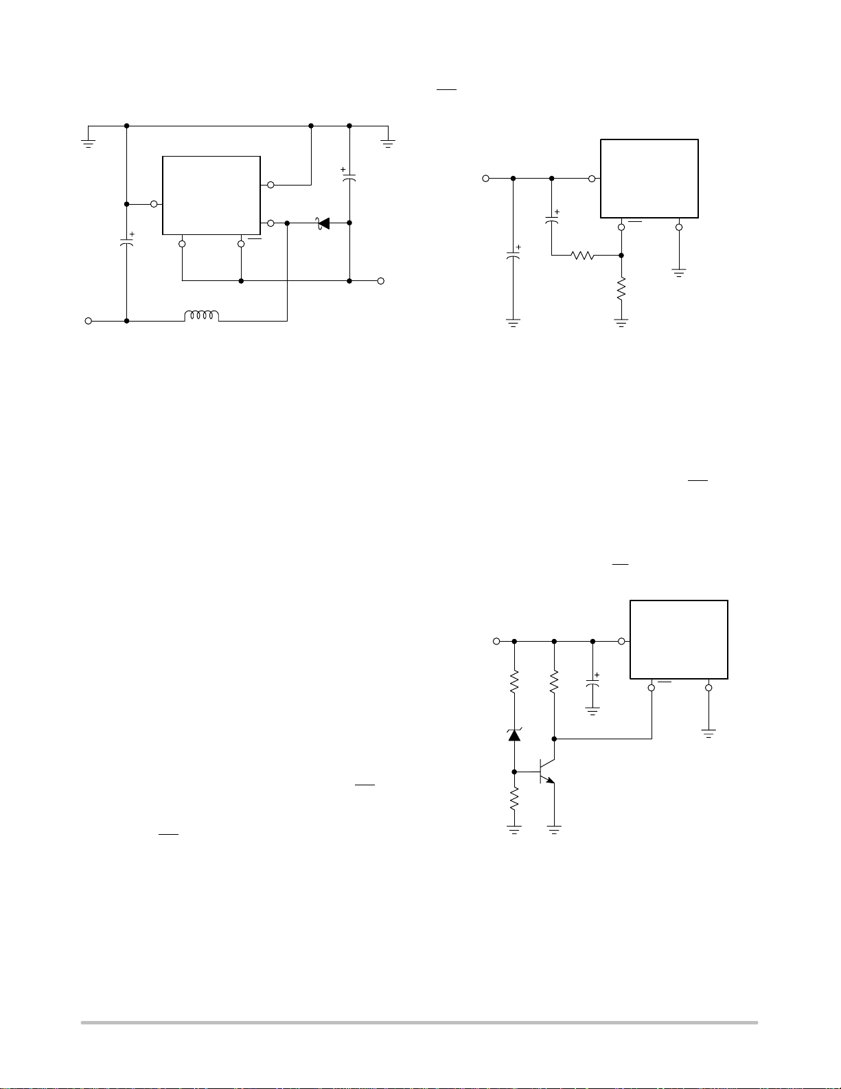
Unregulated
DC Input
12 V to 25 V
100 mF
Figure 25. Inverting Buck−Boost Regulator Using the
+V
in
LM2575−12
1
C
in
/50 V
LM2575−12 Develops −12 V @ 0.35 A
Feedback
4
Output
2
53ON
/OFFGND
L1
100 mH
D1
1N5819
C
out
1800 mF
/16 V
Regulated
Output
−12 V @ 0.35 A
ADDITIONAL APPLICATIONS
Inverting Regulator
An inverting buck−boost regulator using the LM2575−12
is shown in Figure 25. This circuit converts a positive input
voltage to a negative output voltage with a common ground
by bootstrapping the regulators ground to the negative
output voltage. By grounding the feedback pin, the regulator
senses the inverted output voltage and regulates it.
In this example the LM2575−12 is used to generate a
−12 V output. The maximum input voltage in this case
cannot exceed +28 V because the maximum voltage
appearing across the regulator is the absolute sum of the
input and output voltages and this must be limited to a
maximum of 40 V.
This circuit configuration is able to deliver approximately
0.35 A to the output when the input voltage is 12 V or higher.
At lighter loads the minimum input voltage required drops
to approximately 4.7 V, because the buck−boost regulator
topology can produce an output voltage that, in its absolute
value, is either greater or less than the input voltage.
Since the switch currents in this buck−boost configuration
are higher than in the standard buck converter topology, the
available output current is lower.
This type of buck−boost inverting regulator can also
require a larger amount of startup input current, even for
light loads. This may overload an input power source with
a current limit less than 1.5 A.
Such an amount of input startup current is needed for at
least 2.0 ms or more. The actual time depends on the output
voltage and size of the output capacitor.
Because of the relatively high startup currents required by
this inverting regulator topology, the use of a delayed startup
or an undervoltage lockout circuit is recommended.
http://onsemi.com
18
Page 19

Using a delayed startup arrangement, the input capacitor
n
n
can charge up to a higher voltage before the switch−mode
regulator begins to operate.
The high input current needed for startup is now partially
supplied by the input capacitor Cin.
Design Recommendations:
The inverting regulator operates in a different manner
than the buck converter and so a different design procedure
has to be used to select the inductor L1 or the output
capacitor C
out
.
The output capacitor values must be larger than is
normally required for buck converter designs. Low input
voltages or high output currents require a large value output
capacitor (in the range of thousands of mF).
The recommended range of inductor values for the
inverting converter design is between 68 mH and 220 mH. T o
select an inductor with an appropriate current rating, the
inductor peak current has to be calculated.
The following formula is used to obtain the peak inductor
current:
where t
I
peak
on
I
[
+
Vin) |VO|
Load(Vin
|VO|
V
in
x
) |VO|)
1
, and f
f
osc
)
Vinxt
2L
osc
on
1
+ 52 kHz.
Under normal continuous inductor current operating
conditions, the worst case occurs when Vin is minimal.
Note that the voltage appearing across the regulator is the
absolute sum of the input and output voltage, and must not
exceed 40 V.
Unregulated
DC Input
12 V to 25 V
C
in
100 mF
0.1 mF
/50 V
+V
in
LM2575−12
1
C1
R1
47 k
R2
47 k
Figure 26. Inverting Buck−Boost
Regulator with Delayed Startup
35ON/OFF GND
Feedback
4
Output
2
L1
100 mH
D1
1N5819
C
out
1800 mF
/16 V
Regulated
Output
−12 V @ 0.35 A
It has been already mentioned above, that in some
situations, the delayed startup or the undervoltage lockout
features could be very useful. A delayed startup circuit
applied to a buck−boost converter is shown in Figure 26.
Figure 32 in the “Undervoltage Lockout” section describes
an undervoltage lockout feature for the same converter
topology.
LM2575
+V
in
C
in
Shutdown
On
Off
Input
R3
470
5.0 V
0
NOTE: This picture does not show the complete circuit.
100 mF
Figure 27. Inverting Buck−Boost Regulator Shut Dow
Circuit Using an Optocoupler
With the inverting configuration, the use of the ON/OFF
pin requires some level shifting techniques. This is caused
by the fact, that the ground pin of the converter IC is no
longer at ground. Now, the ON/OFF pin threshold voltage
(1.4 V approximately) has to be related to the negative
output voltage level. There are many different possible shut
down methods, two of them are shown in Figures 27 and 28.
R2
5.6 k
Shutdown
Input
+V
Q1
2N3906
+V
+V
in
NOTE: This picture does not show the complete circuit.
Off
0
On
C
in
100 mF
Figure 28. Inverting Buck−Boost Regulator Shut Dow
Circuit Using a PNP Transistor
Negative Boost Regulator
This example is a variation of the buck−boost topology
and is called a negative boost regulator. This regulator
experiences relatively high switch current, especially at low
input voltages. The internal switch current limiting results in
lower output load current capability.
The circuit in Figure 29 shows the negative boost
configuration. The input voltage in this application ranges
from −5.0 V to −12 V and provides a regulated −12 V output.
R1
47 k
MOC8101
in
1
+V
in
1
LM2575−XX
R1
12 k
LM2575−XX
35
ON/OFF
R2
47 k
35 GNDON/OFF
−V
out
GND
−V
out
http://onsemi.com
19
Page 20
LM2575
If the input voltage is greater than −12 V, the output will rise
above −12 V accordingly, but will not damage the regulator.
C
out
1000 mF
/16 V
Regulated
Output
V
= −12 V
out
+V
in
1
C
in
100 mF
/50 V
Unregulated
DC Input
−Vin = −5.0 V to −12 V
LM2575−12
L1
150 mH
4
Feedback
Output
2
53
ON/OFFGND
D1
1N5817
Load Current from
200 mA for Vin = −5.2 V
to 500 mA for Vin = −7.0 V
Figure 29. Negative Boost Regulator
Design Recommendations:
The same design rules as for the previous inverting
buck−boost converter can be applied. The output capacitor
C
must be chosen larger than would be required for a
out
standard buck converter. Low input voltages or high output
currents require a large value output capacitor (in the range
of thousands of mF). The recommended range of inductor
values for the negative boost regulator is the same as for
inverting converter design.
Another important point is that these negative boost
converters cannot provide current limiting load protection in
the event of a short in the output so some other means, such
as a fuse, may be necessary to provide the load protection.
Delayed Startup
There are some applications, like the inverting regulator
already mentioned above, which require a higher amount of
startup current. In such cases, if the input power source is
limited, this delayed startup feature becomes very useful.
To provide a time delay between the time the input voltage
is applied and the time when the output voltage comes up,
the circuit in Figure 30 can be used. As the input voltage is
applied, the capacitor C1 charges up, and the voltage across
the resistor R2 falls down. When the voltage on the ON/OFF
pin falls below the threshold value 1.4 V, the regulator starts
up. Resistor R1 is included to limit the maximum voltage
applied to the ON/OFF pin, reduces the power supply noise
sensitivity, and also limits the capacitor C1 discharge
current, but its use is not mandatory.
When a high 50 Hz or 60 Hz (100 Hz or 120 Hz
respectively) ripple voltage exists, a long delay time can
cause some problems by coupling the ripple into the
ON/OFF pin, the regulator could be switched periodically
on and off with the line (or double) frequency.
+V
in
C
in
100 mF
NOTE: This picture does not show the complete circuit.
Figure 30. Delayed Startup Circuitry
Undervoltage Lockout
+V
C1
0.1 mF
R1
47 k
in
1
LM2575−XX
35 GNDON/OFF
R2
47 k
Some applications require the regulator to remain off until
the input voltage reaches a certain threshold level. Figure 31
shows an undervoltage lockout circuit applied to a buck
regulator. A version of this circuit for buck−boost converter
is shown in Figure 32. Resistor R3 pulls the ON/OFF pin
high and keeps the regulator off until the input voltage
reaches a predetermined threshold level, which is
determined by the following expression:
R2
Vth[ V
+V
in
R2
10 k
1N5242B
10 k
NOTE: This picture does not show the complete circuit.
R3
47 k
Z1
R1
Z1
Q1
2N3904
)
ǒ
Figure 31. Undervoltage Lockout Circuit for
Buck Converter
1 )
R1
+V
in
1
C
in
100 mF
Ǔ
V
BE
LM2575−5.0
Vth ≈ 13 V
(Q1)
35 GNDON/OFF
http://onsemi.com
20
Page 21

+V
in
R2
15 k
Z1
1N5242B
R1
15 k
NOTE: This picture does not show the complete circuit.
R3
68 k
Q1
2N3904
+V
in
1
C
in
100 mF
LM2575−5.0
35 GNDON/OFF
Figure 32. Undervoltage Lockout Circuit for
Buck−Boost Converter
Feedback
Unregulated
DC Input
+
C
100 mF
/50 V
+V
in
LM2575−Adj
1
in
4
Output
2
53ON/OFFGND
Vth ≈ 13 V
V
= −5.0 V
out
150 mH
D1
1N5819
LM2575
Adjustable Output, Low−Ripple Power Supply
A 1.0 A output current capability power supply that
features an adjustable output voltage is shown in Figure 33.
This regulator delivers 1.0 A into 1.2 V to 35 V output.
The input voltage ranges from roughly 8.0 V to 40 V. In order
to achieve a 10 or more times reduction of output ripple, an
additional L−C filter is included in this circuit.
L1
R2
50 k
C
out
2200 mF
R1
1.1 k
L2
20 mH
100 mF
Regulated
Output Voltage
1.2 V to 35 V @1.0 A
C1
Optional Output
Ripple Filter
Figure 33. Adjustable Power Supply with Low Ripple Voltage
JAθ
R , THERMAL RESISTANCE
80
70
60
50
JUNCTION-TO-AIR ( C/W)°
40
30
Free Air
Mounted
Vertically
010203025155.0
P
for TA = 50°C
D(max)
Minimum
Size Pad
R
q
JA
L, LENGTH OF COPPER (mm)
2.0 oz. Copper
L
L
3.5
3.0
2.5
2.0
1.5
1.0
Figure 34. D2PAK Thermal Resistance and Maximum
Power Dissipation versus P.C.B. Copper Length
, MAXIMUM POWER DISSIPATION (W)
P
D
http://onsemi.com
21
Page 22
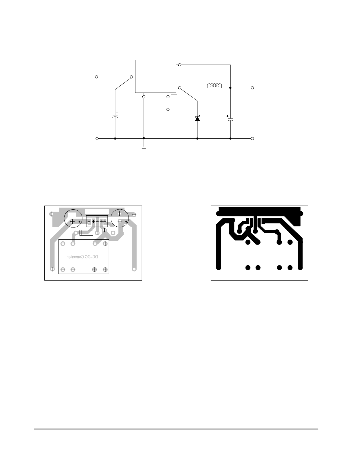
LM2575
THE LM2575−5.0 STEP−DOWN VOLTAGE REGULATOR WITH 5.0 V @ 1.0 A OUTPUT POWER
CAPABILITY. TYPICAL APPLICATION WITH THROUGH−HOLE PC BOARD LAYOUT
Feedback
Unregulated
= +7.0 V to +40 V
+V
in
DC Input
+V
in
1
LM2575−5.0
4
L1
Output
2
330 mH
Regulated Output
+V
= 5.0 V @ 1.0 A
out1
53ON/OFFGND
GND
+V
GND
C1
100 mF
/50 V
in
C1 − 100 mF, 50 V, Aluminium Electrolytic
C2 − 330 mF, 16 V, Aluminium Electrolytic
D1 − 1.0 A, 40 V, Schottky Rectifier, 1N5819
L1 − 330 mH, Tech 39: 77 458 BV, Toroid Core, Through−Hole, Pin 3 = Start, Pin 7 = Finish
J1
D1
1N5819
C
out
330 mF
/16 V
GND
out
Figure 35. Schematic Diagram of the LM2575−5.0 Step−Down Converter
in
L1
in
C1
U1 LM2575
D1
GND
out
J1
C2
DC−DC Converter
+V
out1
NOTE: Not to scale. NOTE: Not to scale.
Figure 36. Printed Circuit Board
Component Side
Figure 37. Printed Circuit Board
Copper Side
http://onsemi.com
22
Page 23

LM2575
THE LM2575−ADJ STEP−DOWN VOLTAGE REGULATOR WITH 8.0 V @ 1.0 A OUTPUT POWER
CAPABILITY. TYPICAL APPLICATION WITH THROUGH−HOLE PC BOARD LAYOUT
Regulated
Output Unfiltered
V
= 8.0 V @1.0 A
out1
4 Feedback
Unregulated
DC Input
+Vin = +10 V to + 40 V
C1
100 mF
/50 V
C1 − 100 mF, 50 V, Aluminium Electrolytic
C2 − 330 mF, 16 V, Aluminium Electrolytic
C3 − 100 mF, 16 V, Aluminium Electrolytic
D1 − 1.0 A, 40 V, Schottky Rectifier, 1N5819
L1 − 330 mH, Tech 39: 77 458 BV, Toroid Core, Through−Hole, Pin 3 = Start, Pin 7 = Finish
L2 − 25 mH, TDK: SFT52501, Toroid Core, Through−Hole
R1 − 1.8 k
R2 − 10 k
Figure 38. Schematic Diagram of the 8.0 V @ 1.0 V Step−Down Converter Using the LM2575−Adj
+V
in
1
LM2575−Adj
Output
2
53ON/OFFGND
330 mH
D1
1N5819
L1
R2
10 k
C2
330 mF
/16 V
R1
1.8 k
V
out
V
ref
R1 is between 1.0 k and 5.0 k
(An additional LC filter is included to achieve low output ripple voltage)
+ V
= 1.23 V
25 mH
100 mF
)ǒ1 )
ref
L2
/16 V
C3
R2
R1
V
Ǔ
Regulated
Output Filtered
= 8.0 V @1.0 A
out2
GND
+V
in
C1
L1
in
U1 LM2575
D1
NOTE: Not to scale. NOTE: Not to scale.
C2
J1
R2 R1
GND
out
C3
L2
+V
out2
+V
out1
Figure 39. PC Board Component Side Figure 40. PC Board Copper Side
References
• National Semiconductor LM2575 Data Sheet and Application Note
• National Semiconductor LM2595 Data Sheet and Application Note
• Marty Brown “Practical Switching Power Supply Design”, Academic Press, Inc., San Diego 1990
• Ray Ridley “High Frequency Magnetics Design”, Ridley Engineering, Inc. 1995
http://onsemi.com
23
Page 24

LM2575
ORDERING INFORMATION
Nominal
Device
Output Voltage
LM2575TV−ADJ
LM2575TV−ADJG
LM2575T−ADJ
LM2575T−ADJG
LM2575D2T−ADJ
1.23 V to 37 V T
LM2575D2T−ADJG
LM2575D2T−ADJR4
LM2575D2T−ADJR4G
LM2575TV−3.3
LM2575TV−3.3G
LM2575T−3.3
LM2575T−3.3G
LM2575D2T−3.3
3.3 V T
LM2575D2T−3.3G
LM2575D2T−3.3R4
LM2575D2T−3.3R4G
LM2575TV−005
LM2575TV−005G
LM2575T−005
LM2575T−005G
LM2575D2T−005
5.0 V T
LM2575D2T−005G
LM2575D2T−5R4
LM2575D2T−5R4G
LM2575TV−012
LM2575TV−012G
LM2575T−012
LM2575T−012G
LM2575D2T−012
12 V T
LM2575D2T−012G
LM2575D2T−12R4
LM2575D2T−12R4G
†For information on tape and reel specifications, including part orientation and tape sizes, please refer to our Tape and Reel Packaging
Specifications Brochure, BRD8011/D.
Operating
Temperature Range
= −40° to +125°C
J
= −40° to +125°C
J
= −40° to +125°C
J
= −40° to +125°C
J
Package Shipping
TO−220 (Vertical Mount)
TO−220 (Vertical Mount)
(Pb−Free)
TO−220 (Straight Lead)
TO−220 (Straight Lead)
(Pb−Free)
D2PAK (Surface Mount)
D2PAK (Surface Mount)
(Pb−Free)
D2PAK (Surface Mount)
D2PAK (Surface Mount)
(Pb−Free)
TO−220 (Vertical Mount)
TO−220 (Vertical Mount)
(Pb−Free)
TO−220 (Straight Lead)
TO−220 (Straight Lead)
(Pb−Free)
D2PAK (Surface Mount)
D2PAK (Surface Mount)
(Pb−Free)
D2PAK (Surface Mount)
D2PAK (Surface Mount)
(Pb−Free)
TO−220 (Vertical Mount)
TO−220 (Vertical Mount)
(Pb−Free)
TO−220 (Straight Lead)
TO−220 (Straight Lead)
(Pb−Free)
D2PAK (Surface Mount)
D2PAK (Surface Mount)
(Pb−Free)
D2PAK (Surface Mount)
D2PAK (Surface Mount)
(Pb−Free)
TO−220 (Vertical Mount)
TO−220 (Vertical Mount)
(Pb−Free)
TO−220 (Straight Lead)
TO−220 (Straight Lead)
(Pb−Free)
D2PAK (Surface Mount)
D2PAK (Surface Mount)
(Pb−Free)
D2PAK (Surface Mount)
D2PAK (Surface Mount)
(Pb−Free)
†
50 Units/Rail
800 Tape & Reel
50 Units/Rail
800 Tape & Reel
50 Units/Rail
800 Tape & Reel
50 Units/Rail
800 Tape & Reel
http://onsemi.com
24
Page 25

LM2575
ORDERING INFORMATION
Nominal
Device Shipping
LM2575TV−015
LM2575TV−015G
LM2575T−015
LM2575T−015G
LM2575D2T−015
LM2575D2T−015G
LM2575D2T−15R4 D2PAK (Surface Mount)
LM2575D2T−15R4G
†For information on tape and reel specifications, including part orientation and tape sizes, please refer to our Tape and Reel Packaging
Specifications Brochure, BRD8011/D.
Output Voltage
15 V T
Operating
Temperature Range
= −40° to +125°C
J
MARKING DIAGRAMS
Package
TO−220 (Vertical Mount)
TO−220 (Vertical Mount)
(Pb−Free)
TO−220 (Straight Lead)
TO−220 (Straight Lead)
(Pb−Free)
D2PAK (Surface Mount)
D2PAK (Surface Mount)
(Pb−Free)
D2PAK (Surface Mount)
(Pb−Free)
†
50 Units/Rail
800 Tape & Reel
TO−220
TV SUFFIX
CASE 314B
LM
2575T−xxx
AWLYWWG
1
TO−220
T SUFFIX
CASE 314D
LM
2575T−xxx
AWLYWWG
5
15
D2PAK
D2T SUFFIX
CASE 936A
LM
2575−xxx
AWLYWWG
15
xxx = 3.3, 5.0, 12, 15, or ADJ
A = Assembly Location
WL = Wafer Lot
Y = Year
WW = Work Week
G = Pb−Free Package
http://onsemi.com
25
Page 26
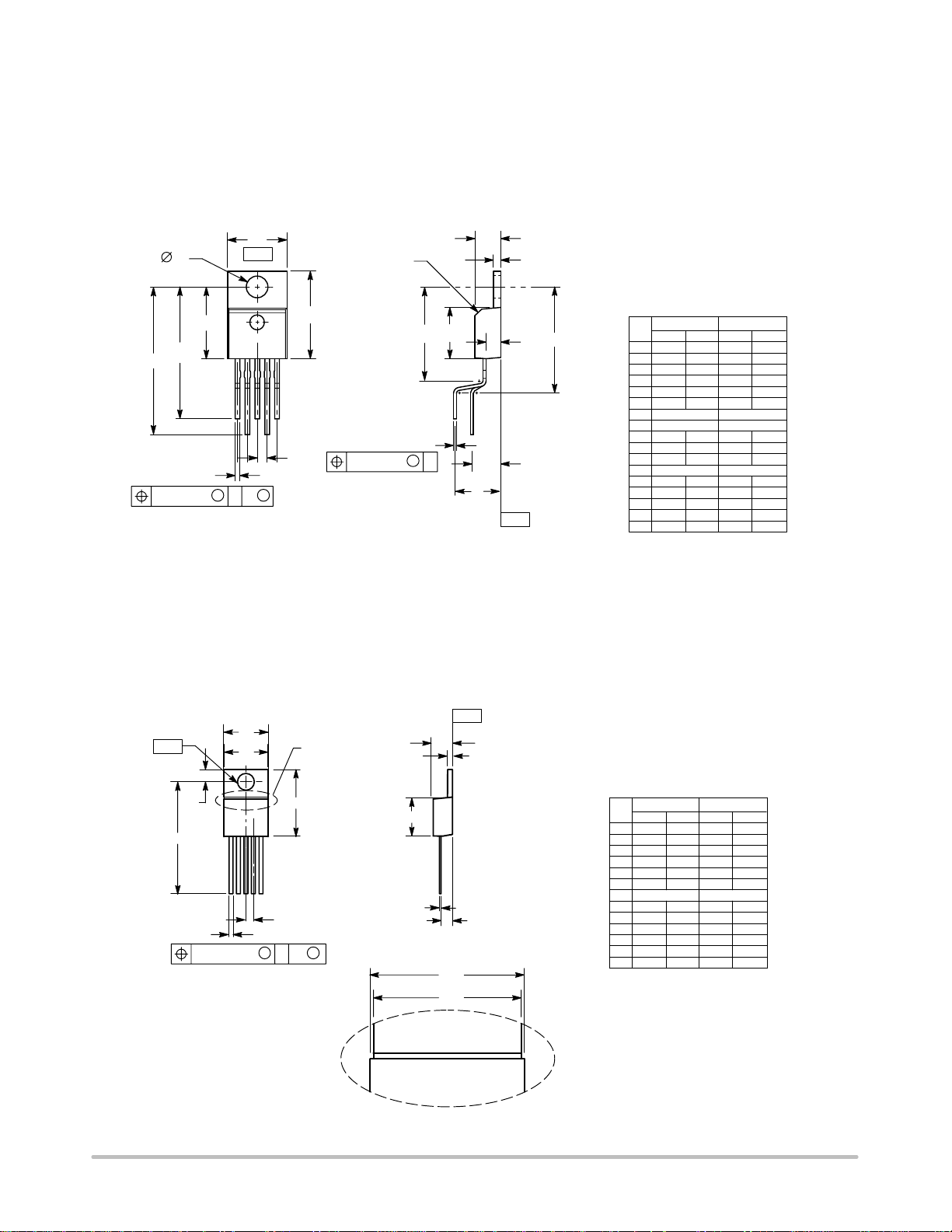
LM2575
PACKAGE DIMENSIONS
TO−220
TV SUFFIX
CASE 314B−05
ISSUE L
Q
U
F
K
5X D
0.10 (0.254) PMT
M
B
−P−
OPTIONAL
CHAMFER
E
A
C
L
S
5X J
G
0.24 (0.610) T
M
H
V
W
N
SEATING
−T−
PLANE
NOTES:
1. DIMENSIONING AND TOLERANCING PER ANSI
Y14.5M, 1982.
2. CONTROLLING DIMENSION: INCH.
3. DIMENSION D DOES NOT INCLUDE
INTERCONNECT BAR (DAMBAR) PROTRUSION.
DIMENSION D INCLUDING PROTRUSION SHALL
NOT EXCEED 0.043 (1.092) MAXIMUM.
DIM MIN MAX MIN MAX
A 0.572 0.613 14.529 15.570
B 0.390 0.415 9.906 10.541
C 0.170 0.180 4.318 4.572
D 0.025 0.038 0.635 0.965
E 0.048 0.055 1.219 1.397
F 0.850 0.935 21.590 23.749
G 0.067 BSC 1.702 BSC
H 0.166 BSC 4.216 BSC
J 0.015 0.025 0.381 0.635
K 0.900 1.100 22.860 27.940
L 0.320 0.365 8.128 9.271
N 0.320 BSC 8.128 BSC
Q 0.140 0.153 3.556 3.886
S −−− 0.620 −−− 15.748
U 0.468 0.505 11.888 12.827
V −−− 0.735 −−− 18.669
W 0.090 0.110 2.286 2.794
MILLIMETERSINCHES
TO−220
T SUFFIX
CASE 314D−04
ISSUE F
−Q−
U
K
D
5 PL
B
B1
12345
0.356 (0.014) T
M
G
DETAIL A−A
A
M
Q
−T−
C
E
L
J
H
B
B1
DETAIL A−A
SEATING
PLANE
NOTES:
1. DIMENSIONING AND TOLERANCING PER ANSI
Y14.5M, 1982.
2. CONTROLLING DIMENSION: INCH.
3. DIMENSION D DOES NOT INCLUDE
INTERCONNECT BAR (DAMBAR) PROTRUSION.
DIMENSION D INCLUDING PROTRUSION SHALL
NOT EXCEED 10.92 (0.043) MAXIMUM.
DIM MIN MAX MIN MAX
A 0.572 0.613 14.529 15.570
B 0.390 0.415 9.906 10.541
B1 0.375 0.415 9.525 10.541
C 0.170 0.180 4.318 4.572
D 0.025 0.038 0.635 0.965
E 0.048 0.055 1.219 1.397
G 0.067 BSC 1.702 BSC
H 0.087 0.112 2.210 2.845
J 0.015 0.025 0.381 0.635
K 0.977 1.045 24.810 26.543
L 0.320 0.365 8.128 9.271
Q 0.140 0.153 3.556 3.886
U 0.105 0.117 2.667 2.972
MILLIMETERSINCHES
http://onsemi.com
26
Page 27

LM2575
PACKAGE DIMENSIONS
D2PAK
D2T SUFFIX
CASE 936A−02
ISSUE C
K
B
D
0.010 (0.254) T
M
C
A
123
45
G
S
H
OPTIONAL
CHAMFER
−T−
TERMINAL 6
E
V
M
L
N
P
R
SOLDERING FOOTPRINT*
8.38
0.33
NOTES:
1. DIMENSIONING AND TOLERANCING PER ANSI
U
Y14.5M, 1982.
2. CONTROLLING DIMENSION: INCH.
3. TAB CONTOUR OPTIONAL WITHIN DIMENSIONS A
AND K.
4. DIMENSIONS U AND V ESTABLISH A MINIMUM
MOUNTING SURFACE FOR TERMINAL 6.
5. DIMENSIONS A AND B DO NOT INCLUDE MOLD
FLASH OR GATE PROTRUSIONS. MOLD FLASH
AND GATE PROTRUSIONS NOT TO EXCEED 0.025
(0.635) MAXIMUM.
DIMAMIN MAX MIN MAX
INCHES
0.386 0.403 9.804 10.236
B 0.356 0.368 9.042 9.347
C 0.170 0.180 4.318 4.572
D 0.026 0.036 0.660 0.914
E 0.045 0.055 1.143 1.397
G 0.067 BSC 1.702 BSC
H 0.539 0.579 13.691 14.707
K 0.050 REF 1.270 REF
L 0.000 0.010 0.000 0.254
M 0.088 0.102 2.235 2.591
N 0.018 0.026 0.457 0.660
P 0.058 0.078 1.473 1.981
R 5 REF
S 0.116 REF 2.946 REF
U 0.200 MIN 5.080 MIN
V 0.250 MIN 6.350 MIN
__
MILLIMETERS
5 REF
1.702
0.067
10.66
0.42
1.016
3.05
0.04
0.12
16.02
0.63
mm
ǒ
SCALE 3:1
inches
Ǔ
*For additional information on our Pb−Free strategy and soldering
details, please download the ON Semiconductor Soldering and
Mounting Techniques Reference Manual, SOLDERRM/D.
http://onsemi.com
27
Page 28

LM2575
ON Semiconductor and are registered trademarks of Semiconductor Components Industries, LLC (SCILLC). SCILLC reserves the right to make changes without further notice
to any products herein. SCILLC makes no warranty, representation or guarantee regarding the suitability of its products for any particular purpose, nor does SCILLC assume any liability
arising out of the application or use of any product or circuit, and specifically disclaims any and all liability, including without limitation special, consequential or incidental damages.
“Typical” parameters which may be provided in SCILLC data sheets and/or specifications can and do vary in different applications and actual performance may vary over time. All
operating parameters, including “Typicals” must be validated for each customer application by customer’s technical experts. SCILLC does not convey any license under its patent rights
nor the rights of others. SCILLC products are not designed, intended, or authorized for use as components in systems intended for surgical implant into the body, or other applications
intended to support or sustain life, or for any other application in which the failure of the SCILLC product could create a situation where personal injury or death may occur. Should
Buyer purchase or use SCILLC products for any such unintended or unauthorized application, Buyer shall indemnify and hold SCILLC and its officers, employees, subsidiaries, affiliates,
and distributors harmless against all claims, costs, damages, and expenses, and reasonable attorney fees arising out of, directly or indirectly, any claim of personal injury or death
associated with such unintended or unauthorized use, even if such claim alleges that SCILLC was negligent regarding the design or manufacture of the part. SCILLC is an Equal
Opportunity/Affirmative Action Employer. This literature is subject to all applicable copyright laws and is not for resale in any manner.
PUBLICATION ORDERING INFORMATION
LITERATURE FULFILLMENT:
Literature Distribution Center for ON Semiconductor
P.O. Box 61312, Phoenix, Arizona 85082−1312 USA
Phone: 480−829−7710 or 800−344−3860 Toll Free USA/Canada
Fax: 480−829−7709 or 800−344−3867 Toll Free USA/Canada
Email: orderlit@onsemi.com
N. American Technical Support: 800−282−9855 Toll Free
USA/Canada
Japan: ON Semiconductor, Japan Customer Focus Center
2−9−1 Kamimeguro, Meguro−ku, Tokyo, Japan 153−0051
Phone: 81−3−5773−3850
http://onsemi.com
ON Semiconductor Website: http://onsemi.com
Order Literature: http://www.onsemi.com/litorder
For additional information, please contact your
local Sales Representative.
LM2575/D
28
 Loading...