

现货库存、技术资料、百科信息、热点资讯,精彩尽在鼎好!
LM339, LM239, LM2901,
LM2901V, NCV2901,
MC3302
Single Supply Quad
Comparators
These comparators are designed for use in level detection, low−level
sensing and memory applications in consumer, automotive, and
industrial electronic applications.
Features
• Single or Split Supply Operation
• Low Input Bias Current: 25 nA (Typ)
• Low Input Offset Current: ±5.0 nA (Typ)
• Low Input Offset Voltage
• Input Common Mode Voltage Range to GND
• Low Output Saturation Voltage: 130 mV (Typ) @ 4.0 mA
• TTL and CMOS Compatible
• ESD Clamps on the Inputs Increase Reliability without Affecting
Device Operation
• NCV Prefix for Automotive and Other Applications Requiring Site
and Control Changes
• Pb−Free Packages are Available
14
14
14
Output 2
Output 1
http://onsemi.com
1
1
1
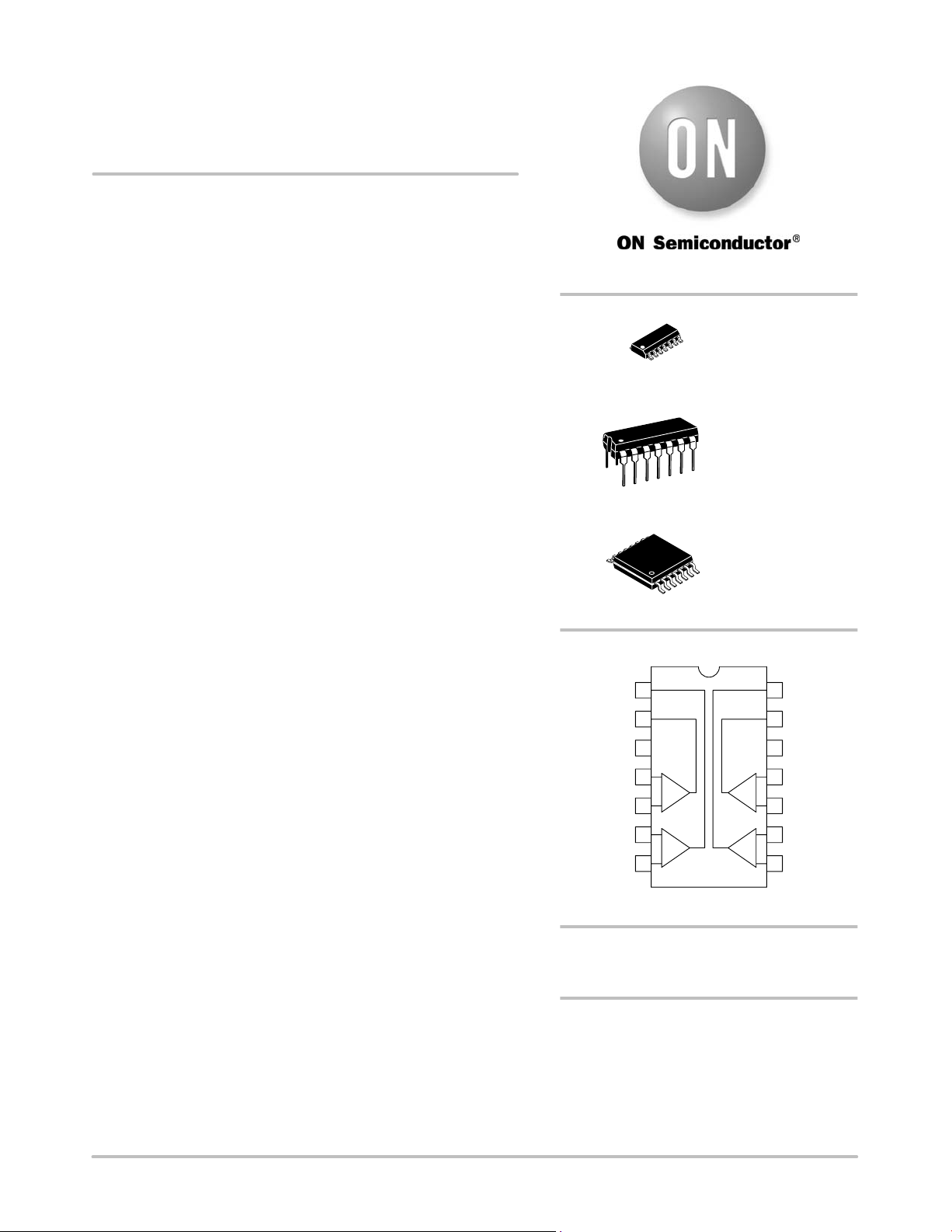
PIN CONNECTIONS
1
2
SOIC−14
D SUFFIX
CASE 751A
PDIP−14
N, P SUFFIX
CASE 646
TSSOP−14
DTB SUFFIX
CASE 948G
14
13
Output 3
Output 4
© Semiconductor Components Industries, LLC, 2007
February, 2007 − Rev. 18
V
CC
− Input 1
+ Input 1
− Input 2
+ Input 2
3
4
*
1
)
5
6
*
2
)
7
(Top View)
12
GND
11
+ Input 4
)
4
*
− Input 4
10
9
+ Input 3
)
3
*
8
− Input 3
ORDERING INFORMATION
See detailed ordering and shipping information in the package
dimensions section on page 6 of this data sheet.
DEVICE MARKING INFORMATION
See general marking information in the device marking
section on page 8 of this data sheet.
1
Publication Order Number:
LM339/D
LM339, LM239, LM2901, LM2901V, NCV2901, MC3302
MAXIMUM RATINGS
Rating Symbol Value Unit
Power Supply Voltage
LM239/LM339/LM2901, V
MC3302
Input Differential Voltage Range
LM239/LM339/LM2901, V
MC3302
Input Common Mode Voltage Range V
Output Short Circuit to Ground (Note 1) I
Power Dissipation @ TA = 25°C
Plastic Package
Derate above 25°C
Junction Temperature T
Operating Ambient Temperature Range
LM239
MC3302
LM2901
LM2901V, NCV2901
LM339
Storage Temperature Range T
ESD Protection at any Pin (Note 2)
Human Body Model
Machine Model
Stresses exceeding Maximum Ratings may damage the device. Maximum Ratings are stress ratings only. Functional operation above the
Recommended Opera t i n g Conditions is not implied. Extended exposure to stresses above the Recommended Operating Conditions may affect
device reliability.
1. The maximum output current m ay b e a s h igh a s 2 0 m A, i ndependent of t he m agnitude o f V
heating and eventual destruction.
2. V
rating for NCV/SC devices is: Human Body Model − 2000 V; Machine Model − 200 V.
ESD
V
CC
Vdc
+36 or ±18
+30 or ±15
V
IDR
Vdc
36
30
ICMR
SC
P
D
−0.3 to V
CC
Continuous
Vdc
1.0
1/R
q
JA
J
T
A
8.0
150 °C
mW/°C
−25 to +85
−40 to +85
−40 to +105
−40 to +125
0 to +70
−65 to +150 °C
V
stg
ESD
1500
200
. Output short circuits to VCC can cause excessive
CC
W
°C
V
V
CC
+ Input
− Input Output
GND
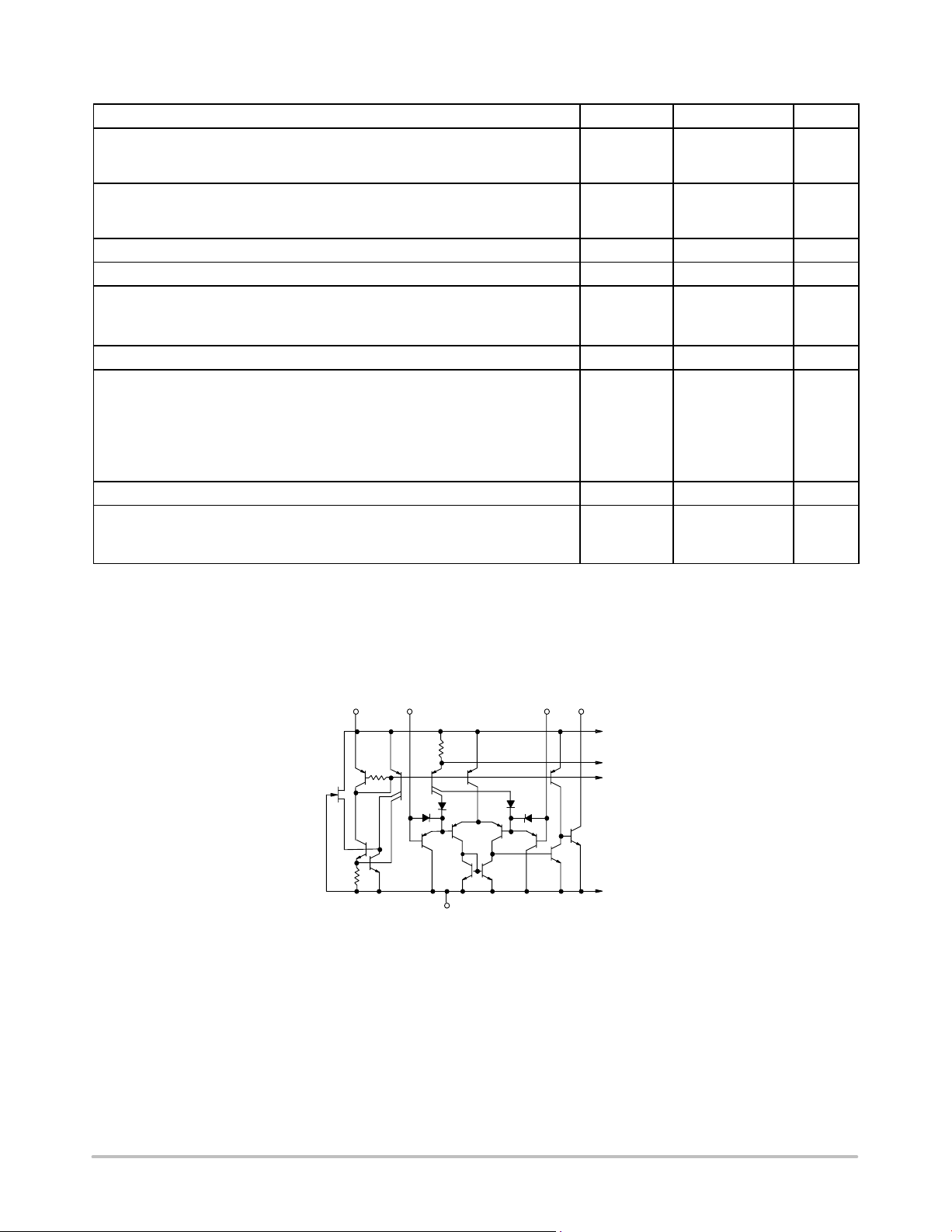
NOTE: Diagram shown is for 1 comparator.
Figure 1. Circuit Schematic
http://onsemi.com
2
LM339, LM239, LM2901, LM2901V, NCV2901, MC3302
ELECTRICAL CHARACTERISTICS (V
= +5.0 Vdc, TA = +25°C, unless otherwise noted)
CC
LM2901/2901V/
Characteristic
Symbol
Input Offset Voltage (Note 4) V
Input Bias Current (Notes 4, 5) I
LM239/339
NCV2901
Min Typ Max Min Typ Max Min Typ Max
IO
IB
− ±2.0 ±5.0 − ±2.0 ±7.0 − ±3.0 ±20 mVdc
− 25 250 − 25 250 − 25 500 nA
MC3302
Unit
(Output in Analog Range)
Input Offset Current (Note 4) I
Input Common Mode Voltage Range V
Supply Current I
IO
ICMR
CC
− ±5.0 ±50 − ±5.0 ±50 − ±3.0 ±100 nA
0 − V
−1.5
CC
0 − V
CC
−1.5
0 − V
CC
−1.5
RL = ∞ (For All Comparators) − 0.8 2.0 − 0.8 2.0 − 0.8 2.0
RL = ∞, VCC = 30 Vdc − 1.0 2.5 − 1.0 2.5 − 1.0 2.5
Voltage Gain A
VOL
50 200 − 25 100 − 25 100 − V/mV
RL ≥ 15 kW, VCC = 15 Vdc
Large Signal Response Time − − 300 − − 300 − − 300 − ns
VI = TTL Logic Swing,
V
= 1.4 Vdc, VRL = 5.0 Vdc,
ref
RL = 5.1 kW
Response Time (Note 6) − − 1.3 − − 1.3 − − 1.3 −
VRL = 5.0 Vdc, RL = 5.1 kW
Output Sink Current I
V
(−) ≥ +1.0 Vdc, VI(+) = 0,
I
Sink
6.0 16 − 6.0 16 − 6.0 16 − mA
VO ≤ 1.5 Vdc
Saturation Voltage V
sat
− 130 400 − 130 400 − 130 500 mV
VI(−) ≥ +1.0 Vdc, VI(+) = 0,
≤ 4.0 mA
I
sink
Output Leakage Current I
OL
− 0.1 − − 0.1 − − 0.1 − nA
VI(+) ≥ +1.0 Vdc, VI(−) = 0,
VO = +5.0 Vdc
3. (LM239) T
(LM339) T
(MC3302) T
(LM2901) T
(LM2901V & NCV2901) T
NCV2901 is qualified for automotive use.
4. At the output switch point, V
(0 Vdc to V
5. The bias current flows out of the inputs due to the PNP input stage. This current is virtually constant, independent of the output state.
= −25°C, T
low
= 0°C, T
low
= −40°C, T
low
= −40°C, T
low
−1.5 Vdc).
CC
= +85°
high
= +70°C
high
= +85°C
high
= +105°
high
= −40°C, T
low
] 1.4 Vdc, RS ≤ 100 W 5.0 Vdc ≤ VCC ≤ 30 Vdc, with the inputs over the full common mode range
O
= +125°C
high
6. The response time specified is for a 100 mV input step with 5.0 mV overdrive. For larger signals, 300 ns is typical.
V
mA
ms
http://onsemi.com
3
LM339, LM239, LM2901, LM2901V, NCV2901, MC3302
PERFORMANCE CHARACTERISTICS (V
= +5.0 Vdc, TA = T
CC
low
to T
[Note 7])
high
LM2901/2901V/
Characteristic Symbol
Input Offset Voltage (Note 8) V
Input Bias Current (Notes 8, 9) I
LM239/339
NCV2901
Min Typ Max Min Typ Max Min Typ Max
IO
IB
− − ±9.0 − − ±15 − − ±40 mVdc
− − 400 − − 500 − − 1000 nA
MC3302
Unit
(Output in Analog Range)
Input Offset Current (Note 8) I
Input Common Mode Voltage Range V
Saturation Voltage V
IO
ICMR
sat
− − ±150 − − ±200 − − ±300 nA
0 − V
−2.0
CC
0 − V
CC
−2.0
0 − V
CC
−2.0
− − 700 − − 700 − − 700 mV
VI(−) ≥ +1.0 Vdc, VI(+) = 0,
I
≤ 4.0 mA
sink
Output Leakage Current I
OL
− − 1.0 − − 1.0 − − 1.0
VI(+) ≥ +1.0 Vdc, VI(−) = 0,
VO = 30 Vdc
Differential Input Voltage V
ID
− − V
CC
− − V
CC
− − V
CC
All VI ≥ 0 Vdc
7. (LM239) T
(LM339) T
(MC3302) T
(LM2901) T
(LM2901V & NCV2901) T
NCV2901 is qualified for automotive use.
8. At the output switch point, V
(0 Vdc to V
9. The bias current flows out of the inputs due to the PNP input stage. This current is virtually constant, independent of the output state.
= −25°C, T
low
= 0°C, T
low
= −40°C, T
low
= −40°C, T
low
−1.5 Vdc).
CC
= +85°
high
= +70°C
high
= +85°C
high
= +105°
high
= −40°C, T
low
] 1.4 Vdc, RS ≤ 100 W 5.0 Vdc ≤ VCC ≤ 30 Vdc, with the inputs over the full common mode range
O
= +125°C
high
10.The response time specified is for a 100 mV input step with 5.0 mV overdrive. For larger signals, 300 ns is typical.
V
mA
Vdc
+ V
+ V
CC
+ V
CC
R3
V
in
R
CC
ref
V
ref
10k
R1
−
+
R2
1.0 M
10 k
10 k
VCC R1
V
[
ref
R
ref
R3 ] R1 / / R
R1 / / R
=
V
H
R1/ / R
V
O
+ R1
ref
ref
/ / R2
ref
+ R2
[V
O(max)
− V
O(min)
R2 ơ Rref / / R1
Figure 2. Inverting Comparator
with Hysteresis
R
ref
V
ref
R1
Vi
R2
n
10 k
−
+
R3
1.0 M
]
10 k
V
O
V
CC
V
=
ref
R
ref
R2 [ R1 / / R
ref
Amount of Hysteresis V
R2
VH =
R2 + R3
[(V
O(max)
R1
+ R1
H
− V
]
O(min)
Figure 3. Noninverting Comparator
with Hysteresis
http://onsemi.com
4
LM339, LM239, LM2901, LM2901V, NCV2901, MC3302
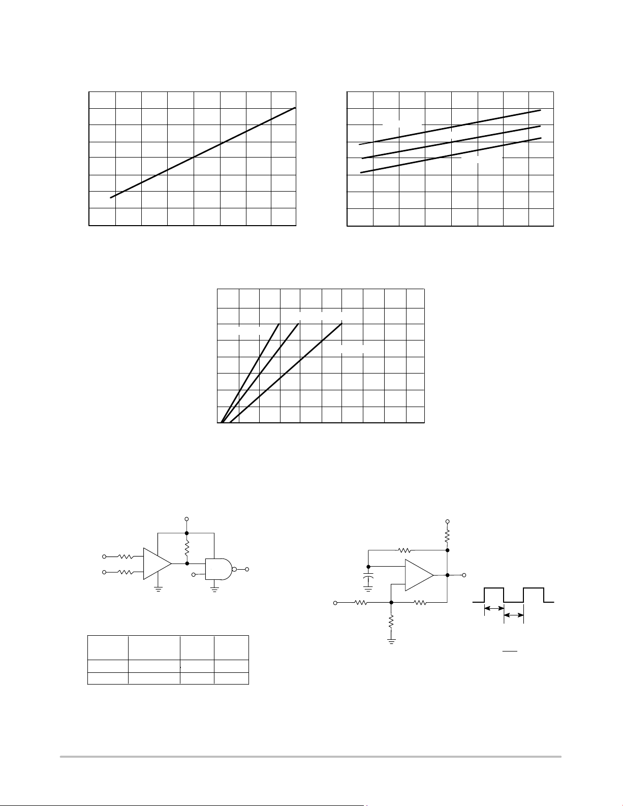
Typical Characteristics
(VCC = 15 Vdc, TA = +25°C (each comparator) unless otherwise noted.)
1.40
1.20
1.00
0.80
NORMALIZED OFFSET VOLTAGE
0.60
48
42
36
TA = −55° C
TA = +25° C
30
T
24
= +125°C
A
18
12
IB,
I INPUT BIAS CURRENT (nA)
6.0
−50 −25 0 25 50 75 100 125
0
0 4.0 8.0 12 16 20 24 28 32
TA, AMBIENT TEMPERATURE (°C) VCC, POWER SUPPLY VOLTAGE (Vdc)
Figure 4. Normalized Input Offset Voltage Figure 5. Input Bias Current
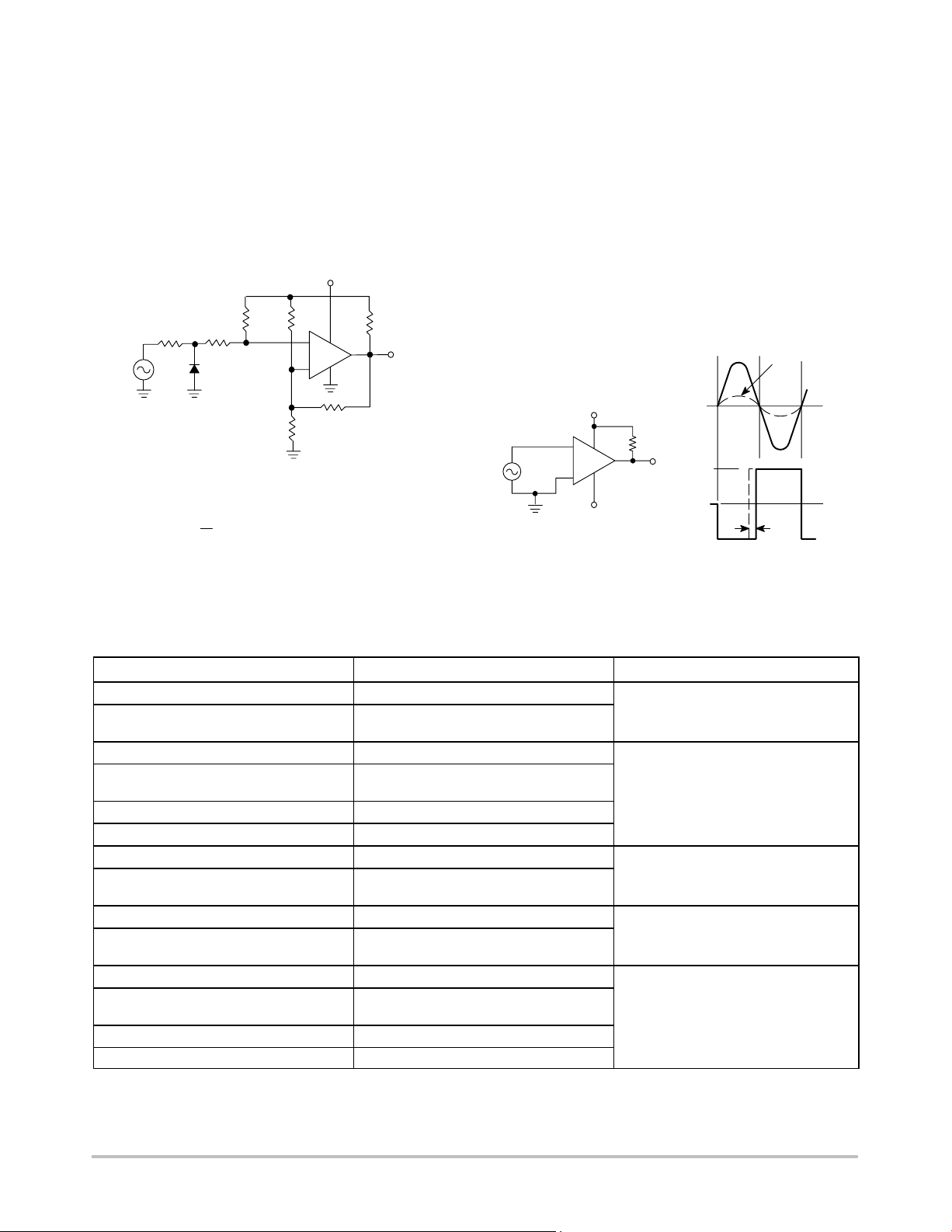
8.0
7.0
6.0
TA = −55° C
5.0
4.0
3.0
O
2.0
I , OUTPUT CURRENT (mA)
1.0
0
0
100 200 300 400 500
V
, OUTPUT SATURATION VOLTAGE (mV)
sat
TA = +25° C
TA = +125°C
Figure 6. Output Sink Current versus
Output Saturation Voltage
V
R
V
in
V
ref
S
R1
R
= Source Resistance
S
R1 ] R
Logic Device
CMOS
TTL
1/4 MC14001
1/4 MC7400
CC
R
+
−
S
L
V
CC
(V)
+15
+5.0
R
kW
100
10
+
C
V
CC
L
R2
330 k
100 k
R4 330 k
R1
−
+
VCC ≥ 4.0 V
R3
330 k
Figure 7. Driving Logic Figure 8. Squarewave Oscillator
10 k
V
O
V
CC
T1 = T2 = 0.69 RC
R2 = R3 = R4
R1 [ R2 // R3 // R4
T1
f [
T2
7.2
C(mF)
http://onsemi.com
5
LM339, LM239, LM2901, LM2901V, NCV2901, MC3302
APPLICATIONS INFORMATION
These quad comparators feature high gain, wide
bandwidth characteristics. This gives the device oscillation
tendencies if the outputs are capacitively coupled to the
inputs via stray capacitance. This oscillation manifests itself
during output transitions (V
to VOH). To alleviate this
OL
situation input resistors < 10 kW should be used. The
+15 V
R1
8.2 k
V
in
D1
D1 prevents input from going negative by more than 0.6 V.
R3 ≤R5for small error in zero crossing
R4
220 k
6.8 k
R2
10
Figure 9. Zero Crossing Detector
(Single Supply)
R5
220 k
15 k
R3
R1 + R2 = R3
10 k
*
)
10 M
V
O
addition of positive feedback (< 10 mV) is also
recommended. It is good design practice to ground all
unused input pins.
Differential input voltages may be larger than supply
voltages without damaging the comparator’s inputs.
Voltages more negative than −300 mV should not be used.
V
≈ 0.4 V peak for 1% phase distortion (Dq).
in(min)
V
V
in
V
CC
*
V
in
+
V
EE
10 k
V
O
V
CC
V
O
V
EE
Figure 10. Zero Crossing Detector
(Split Supplies)
in(min)
q
q
Dq
ORDERING INFORMATION
Device Package Shipping
LM239D SOIC−14
LM239DG SOIC−14
(Pb−Free)
LM239DR2 SOIC−14
LM239DR2G SOIC−14
(Pb−Free)
LM239DTBR2 TSSOP−14*
LM239DTBR2G TSSOP−14*
LM239N PDIP−14
LM239NG PDIP−14
(Pb−Free)
LM339D SOIC−14
LM339DG SOIC−14
(Pb−Free)
LM339DR2 SOIC−14
LM339DR2G SOIC−14
(Pb−Free)
LM339DTBR2 TSSOP−14*
LM339DTBR2G TSSOP−14*
†For information on tape and reel specifications, including part orientation and tape sizes, please refer to our Tape and Reel Packaging
Specifications Brochure, BRD8011/D.
*This package is inherently Pb−Free.
55 Units/Tube
2500 / Tape & Reel
25 Units/Rail
55 Units/Tube
2500 / Tape & Reel
†
http://onsemi.com
6
LM339, LM239, LM2901, LM2901V, NCV2901, MC3302
ORDERING INFORMATION
Device Shipping
LM339N PDIP−14
LM339NG PDIP−14
LM2901D SOIC−14
LM2901DG SOIC−14
LM2901DR2 SOIC−14
LM2901DR2G SOIC−14
LM2901DTBR2 TSSOP−14*
LM2901DTBR2G TSSOP−14*
LM2901N PDIP−14
LM2901NG PDIP−14
LM2901VD SOIC−14
LM2901VDG SOIC−14
LM2901VDR2 SOIC−14
LM2901VDR2G SOIC−14
LM2901VDTBR2 TSSOP−14*
LM2901VDTBR2G TSSOP−14*
LM2901VN PDIP−14
LM2901VNG PDIP−14
NCV2901DR2 SOIC−14
NCV2901DR2G SOIC−14
NCV2901DTBR2G TSSOP−14*
NCV2901CTR Bare Die 6000 / Tape & Reel
MC3302D SOIC−14
MC3302DG SOIC−14
MC3302DR2 SOIC−14
MC3302DR2G SOIC−14
MC3302DTBR2 TSSOP−14*
MC3302DTBR2G TSSOP−14*
MC3302P PDIP−14
MC3302PG PDIP−14
†For information on tape and reel specifications, including part orientation and tape sizes, please refer to our Tape and Reel Packaging
Specifications Brochure, BRD8011/D.
*This package is inherently Pb−Free.
Package
(Pb−Free)
(Pb−Free)
(Pb−Free)
(Pb−Free)
(Pb−Free)
(Pb−Free)
(Pb−Free)
(Pb−Free)
(Pb−Free)
(Pb−Free)
(Pb−Free)
25 Units/Rail
55 Units/Rail
2500 / Tape & Reel
25 Units/Rail
55 Units/Tube
2500 / Tape & Reel
25 Units/Rail
2500 / Tape & Reel
55 Units/Tube
2500 / Tape & Reel
25 Units/Rail
†
http://onsemi.com
7

LM339, LM239, LM2901, LM2901V, NCV2901, MC3302
MARKING DIAGRAMS
PDIP−14
N, P SUFFIX
CASE 646
14
14
LM339N
AWLYYWWG
LM339DG
AWLYWW
1
14
1
239
ALYWG
G
AWLYYWWG
14
1
14
1
LM239N
LM239DG
AWLYWW
339
ALYWG
G
111
14
1
LM2901N
AWLYYWWG
SOIC−14
D SUFFIX
CASE 751A
LM2901DG
AWLYWW
TSSOP−14
DTB SUFFIX
CASE 948G
14
ALYWG
1
2901
G
141414
1
14
1
14
1
LM2901VN
AWLYYWWG
LM2901VDG
AWLYWW
2901
V
ALYWG
G
14114
MC3302P
AWLYYWWG
14
*
*
MC3302DG
AWLYWW
1
14
3302
ALYWG
G
1
A = Assembly Location
WL, L = Wafer Lot
YY, Y = Year
WW, W = Work Week
G or G = Pb−Free Package
(Note: Microdot may be in either location)
*This marking diagram also applies to NCV2901.
http://onsemi.com
8

−T−
SEATING
PLANE
14 8
17
N
HG
LM339, LM239, LM2901, LM2901V, NCV2901, MC3302
PACKAGE DIMENSIONS
PDIP−14
CASE 646−06
ISSUE P
NOTES:
1. DIMENSIONING AND TOLERANCING PER ANSI
Y14.5M, 1982.
2. CONTROLLING DIMENSION: INCH.
B
A
F
L
C
D
14 PL
0.13 (0.005)
K
J
M
M
3. DIMENSION L TO CENTER OF LEADS WHEN
FORMED PARALLEL.
4. DIMENSION B DOES NOT INCLUDE MOLD FLASH.
5. ROUNDED CORNERS OPTIONAL.
DIM MIN MAX MIN MAX
A 0.715 0.770 18.16 19.56
B 0.240 0.260 6.10 6.60
C 0.145 0.185 3.69 4.69
D 0.015 0.021 0.38 0.53
F 0.040 0.070 1.02 1.78
G 0.100 BSC 2.54 BSC
H 0.052 0.095 1.32 2.41
J 0.008 0.015 0.20 0.38
K 0.115 0.135 2.92 3.43
L
0.290 0.310 7.37 7.87
M −−− 10 −−− 10
N 0.015 0.039 0.38 1.01
__
MILLIMETERSINCHES
http://onsemi.com
9

−T−
SEATING
PLANE
LM339, LM239, LM2901, LM2901V, NCV2901, MC3302
PACKAGE DIMENSIONS
SOIC−14
CASE 751A−03
ISSUE H
NOTES:
1. DIMENSIONING AND TOLERANCING PER
−A−
14
1
8
−B−
7
P
7 PL
0.25 (0.010) B
M
M
G
F
J
D 14 PL
0.25 (0.010) A
M
T
R
X 45
C
K
S
B
S
_
M
SOLDERING FOOTPRINT*
7X
7.04
1
14X
0.58
14X
1.52
ANSI Y14.5M, 1982.
2. CONTROLLING DIMENSION: MILLIMETER.
3. DIMENSIONS A AND B DO NOT INCLUDE
MOLD PROTRUSION.
4. MAXIMUM MOLD PROTRUSION 0.15 (0.006)
PER SIDE.
5. DIMENSION D DOES NOT INCLUDE
DAMBAR PROTRUSION. ALLOWABLE
DAMBAR PROTRUSION SHALL BE 0.127
(0.005) TOTAL IN EXCESS OF THE D
DIMENSION AT MAXIMUM MATERIAL
CONDITION.
DIM MIN MAX MIN MAX
A 8.55 8.75 0.337 0.344
B 3.80 4.00 0.150 0.157
C 1.35 1.75 0.054 0.068
D 0.35 0.49 0.014 0.019
F 0.40 1.25 0.016 0.049
G 1.27 BSC 0.050 BSC
J 0.19 0.25 0.008 0.009
K 0.10 0.25 0.004 0.009
M 0 7 0 7
__ __
P 5.80 6.20 0.228 0.244
R 0.25 0.50 0.010 0.019
INCHESMILLIMETERS
1.27
PITCH
DIMENSIONS: MILLIMETERS
*For additional information on our Pb−Free strategy and soldering
details, please download the ON Semiconductor Soldering and
Mounting Techniques Reference Manual, SOLDERRM/D.
http://onsemi.com
10
LM339, LM239, LM2901, LM2901V, NCV2901, MC3302
TSSOP−14
PACKAGE DIMENSIONS
CASE 948G−01
ISSUE B
0.10 (0.004)
−T−
SEATING
PLANE
14X REFK
B
−U−
S
U
T
S
N
0.25 (0.010)
M
N
F
DETAIL E
K
K1
J
J1
M
8
U0.15 (0.006) T
S
2X L/2
0.10 (0.004) V
14
L
PIN 1
IDENT.
1
S
U0.15 (0.006) T
A
−V−
7
SECTION N−N
C
D
G
H
DETAIL E
NOTES:
1. DIMENSIONING AND TOLERANCING PER
ANSI Y14.5M, 1982.
2. CONTROLLING DIMENSION: MILLIMETER.
3. DIMENSION A DOES NOT INCLUDE MOLD
FLASH, PROTRUSIONS OR GATE BURRS.
MOLD FLASH OR GATE BURRS SHALL NOT
EXCEED 0.15 (0.006) PER SIDE.
4. DIMENSION B DOES NOT INCLUDE
INTERLEAD FLASH OR PROTRUSION.
INTERLEAD FLASH OR PROTRUSION SHALL
NOT EXCEED 0.25 (0.010) PER SIDE.
5. DIMENSION K DOES NOT INCLUDE DAMBAR
PROTRUSION. ALLOWABLE DAMBAR
PROTRUSION SHALL BE 0.08 (0.003) TOTAL
IN EXCESS OF THE K DIMENSION AT
MAXIMUM MATERIAL CONDITION.
6. TERMINAL NUMBERS ARE SHOWN FOR
REFERENCE ONLY.
7. DIMENSION A AND B ARE TO BE
DETERMINED AT DATUM PLANE −W−.
INCHESMILLIMETERS
−W−
DIM MIN MAX MIN MAX
A 4.90 5.10 0.193 0.200
B 4.30 4.50 0.169 0.177
C −−− 1.20 −−− 0.047
D 0.05 0.15 0.002 0.006
F 0.50 0.75 0.020 0.030
G 0.65 BSC 0.026 BSC
H 0.50 0.60 0.020 0.024
J 0.09 0.20 0.004 0.008
J1 0.09 0.16 0.004 0.006
K 0.19 0.30 0.007 0.012
K1 0.19 0.25 0.007 0.010
L 6.40 BSC 0.252 BSC
M 0 8 0 8
____
SOLDERING FOOTPRINT*
7.06
1
14X
0.36
*For additional information on our Pb−Free strategy and soldering
details, please download the ON Semiconductor Soldering and
Mounting Techniques Reference Manual, SOLDERRM/D.
14X
1.26
DIMENSIONS: MILLIMETERS
0.65
PITCH
http://onsemi.com
11

LM339, LM239, LM2901, LM2901V, NCV2901, MC3302
ON Semiconductor and are registered trademarks of Semiconductor Components Industries, LLC (SCILLC). SCILLC reserves the right to make changes without further notice
to any products herein. SCILLC makes no warranty, representation or guarantee regarding the suitability of its products for any particular purpose, nor does SCILLC assume any liability
arising out of the application or use of any product or circuit, and specifically disclaims any and all liability, including without limitation special, consequential or incidental damages.
“Typical” parameters which may be provided in SCILLC data sheets and/or specifications can and do vary in different applications and actual performance may vary over time. All
operating parameters, including “Typicals” must be validated for each customer application by customer’s technical experts. SCILLC does not convey any license under its patent rights
nor the rights of others. SCILLC products are not designed, intended, or authorized for use as components in systems intended for surgical implant into the body, or other applications
intended to support or sustain life, or for any other application in which the failure of the SCILLC product could create a situation where personal injury or death may occur. Should
Buyer purchase or use SCILLC products for any such unintended or unauthorized application, Buyer shall indemnify and hold SCILLC and its officers, employees, subsidiaries, affiliates,
and distributors harmless against all claims, costs, damages, and expenses, and reasonable attorney fees arising out of, directly or indirectly, any claim of personal injury or death
associated with such unintended or unauthorized use, even if such claim alleges that SCILLC was negligent regarding the design or manufacture of the part. SCILLC is an Equal
Opportunity/Affirmative Action Employer. This literature is subject to all applicable copyright laws and is not for resale in any manner.
PUBLICATION ORDERING INFORMATION
LITERATURE FULFILLMENT:
Literature Distribution Center for ON Semiconductor
P.O. Box 5163, Denver, Colorado 80217 USA
Phone: 303−675−2175 or 800−344−3860 Toll Free USA/Canada
Fax: 303−675−2176 or 800−344−3867 Toll Free USA/Canada
Email: orderlit@onsemi.com
N. American Technical Support: 800−282−9855 Toll Free
USA/Canada
Europe, Middle East and Africa Technical Support:
Phone: 421 33 790 2910
Japan Customer Focus Center
Phone: 81−3−5773−3850
http://onsemi.com
ON Semiconductor Website: www.onsemi.com
Order Literature: http://www.onsemi.com/orderlit
For additional information, please contact your local
Sales Representative
LM339/D
12
 Loading...