

Page 1
LC87F1MADG1AGEVK
LC87F1M16A Evaluation
Board User's Manual
http://onsemi.com
EVAL BOARD USER’S MANUAL
Summary
This document describes the specification of this product
“LC87F1MADG1AGEVK”, and it uses the following
software.
Table 1. SUMMARY
Kind of Software Name of the Software
Microcontroller LC87F1M16A Version 0x1000
Application for PC LC87F1MADG1AGEVK_Application.exe
Driver LC87F1MADG1AGEVK_driver.inf
Content
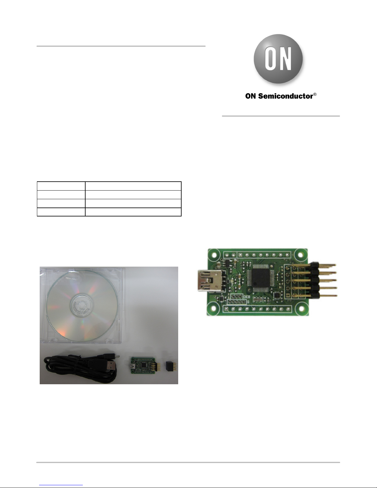
Evaluation Board (USB−DG1−1Ma1−EVK): 1
USB-mini Cable: 1
Connector (FSS−43085−05 HIROSUGI−KEIKI): 1
CD-ROM*: 1
About Application
Required OS: Windows XP or later
Profile Needed: .NET Framework4 Client Profile
Summary of the Product
This product is for data receiving/transmitting by
changing the various input/output formats listed below from
PC to device and vice versa.
2
• I
C
• SPI
• PWM
• Digital Input/Output (GPIO)
• ADC
* Please use the included CD-ROM for the documentations, driver
for this software, application software, and sample application
software.
© Semiconductor Components Industries, LLC, 2014
February, 2014 − Rev. 3
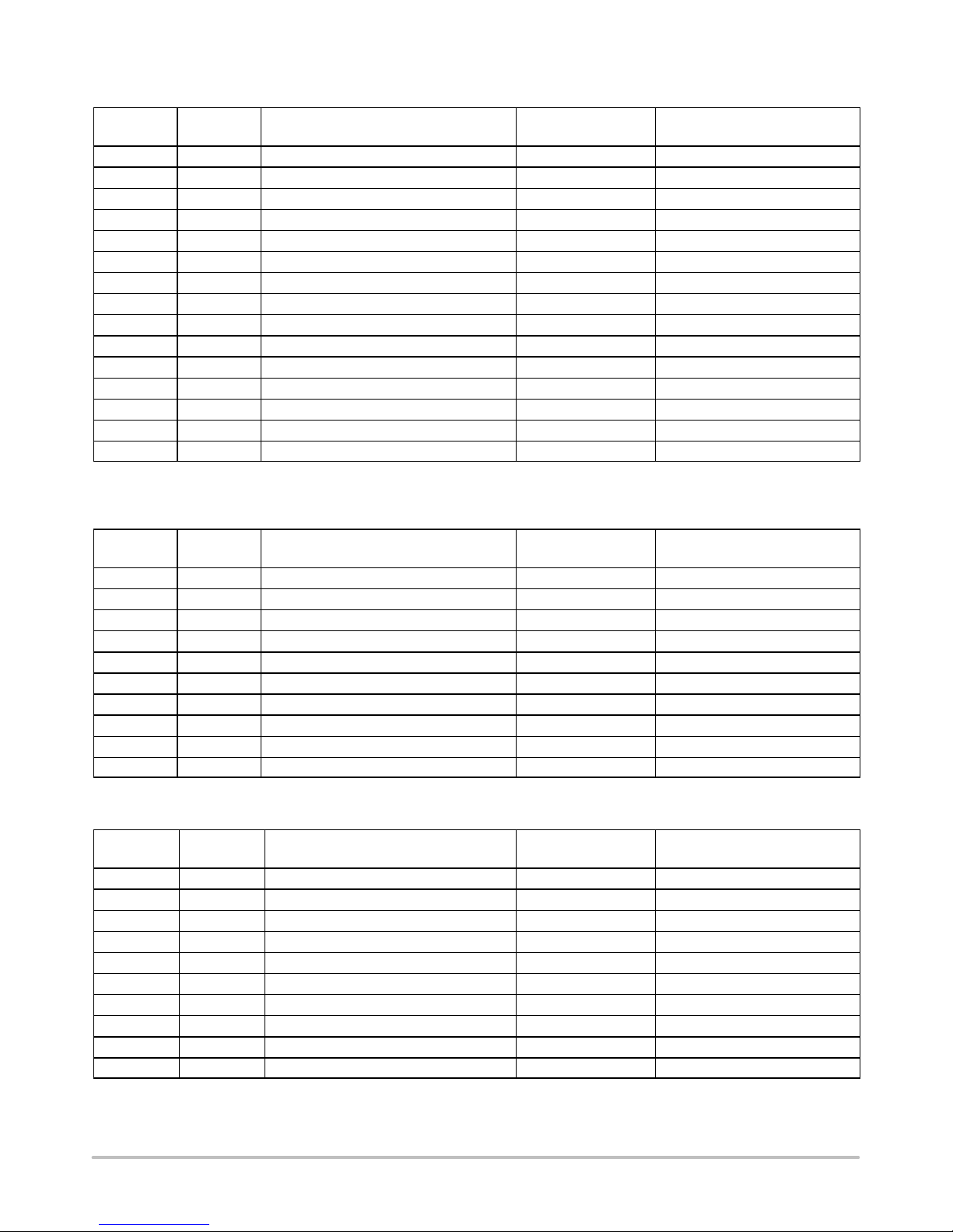
Figure 1. LC87F1M16A
1 Publication Order Number:
EVBUM2170/D
Page 2

LC87F1MADG1AGEVK
COMPOSITION OF THIS PRODUCT
Figure 2. Composition
http://onsemi.com
2
Page 3

CONNECTION DIAGRAM WHEN USE
* PC, Device and Interface cable is not included.
LC87F1MADG1AGEVK
Figure 3. Connection Diagram
http://onsemi.com
3
Page 4

USB Mini
Cable Terminal
LC87F1MADG1AGEVK
SUMMARY OF THE PINS ON THE PRODUCT
GPIO10
GPIO12
GPIO13
GPIO14
GPIO15
GND
+5V
Extension Terminal 1
Extension Terminal 2
GPIO19
GPIO18
GPIO17
GPIO16
Extension 0
GPIO20
GPIO11
GPIO9
PWM2
Extension 2
Extension 1
GPIO8
PWM3
Interface Cable Terminal
USB-Mini Cable Terminal
USB2.0 compliant
Corresponding to Full Speed (12 Mbps)
Please connect the USB-Mini cable terminal to the PC
using the included USB-Mini cable.
PWM1 PWM0 SO
GPIO7 GPIO3 SI
GPIO6 GPIO2 CK
GPIO5 GPIO1 GND
GPIO4 GPIO0 VDD
Figure 4. Summary of the Pins
LED
Initial state of the LED is OFF.
It will light-up when driver is installed and USB
communication is established. After that, it will light-up
once every one communication with the data.
http://onsemi.com
4
Page 5
LC87F1MADG1AGEVK
Table 2. INTERFACE CABLE TERMINAL
Name
of the Pin
SO O SIO − Refer to the Micro’s Catalogue
SI I/O SIO 0 to 3.3 V Refer to the Micro’s Catalogue
CK I/O SIO 0 to 3.3 V Refer to the Micro’s Catalogue
GND − − − −
VDD − − − 100 mA
PWM0 O PWM − Refer to the Micro’s Catalogue
PWM1 O PWM − Refer to the Micro’s Catalogue
GPIO0 I/O Open, Internal Pull-Up, Low, High 0 to 3.3 V Refer to the Micro’s Catalogue
GPIO1 I/O Open, Internal Pull-Up, Low, High 0 to 3.3 V Refer to the Micro’s Catalogue
GPIO2 I/O Open, Internal Pull-Up, Low, High 0 to 3.3 V Refer to the Micro’s Catalogue
GPIO3 I/O Open, Internal Pull-Up, Low, High 0 to 3.3 V Refer to the Micro’s Catalogue
GPIO4 I/O Open, Internal Pull-Up, Low, High 0 to 3.3 V Refer to the Micro’s Catalogue
GPIO5 I/O Open, Internal Pull-Up, Low, High 0 to 3.3 V Refer to the Micro’s Catalogue
GPIO6 I/O Open, Internal Pull-Up, Low, High 0 to 3.3 V Refer to the Micro’s Catalogue
GPIO7 I/O Open, Internal Pull-Up, Low, High 0 to 3.3 V Refer to the Micro’s Catalogue
NOTE: Internal pull-up is connected to 3.3 V through 18 k to 150 kW inside of the microcontroller.
I/O Setting
State of the Possible Setting
of the Terminal
Input Voltage Range Max. Output Current
Table 3. EXTENSION TERMINAL 1
Name
of the Pin
GPIO8 I/O Open, Internal Pull-Up, Low, High 0 to 3.3 V Refer to the Micro’s Catalogue
GPIO9 I/O Open, Internal Pull-Up, Low, High 0 to 3.3 V Refer to the Micro’s Catalogue
GPIO10 I/O Open, Internal Pull-Up, Low, High 0 to 3.3 V Refer to the Micro’s Catalogue
GPIO11 I/O Open, Internal Pull-Up, Low, High 0 to 3.3V Refer to the Micro’s Catalogue
GPIO12 I/O Open, Internal Pull-Up, Low, High 0 to 3.3 V Refer to the Micro’s Catalogue
GPIO13 I/O Open, Internal Pull-Up, Low, High 0 to 3.3 V Refer to the Micro’s Catalogue
GPIO14 I/O Open, Internal Pull-Up, Low, High 0 to 3.3 V Refer to the Micro’s Catalogue
GPIO15 I/O Open, Internal Pull-Up, Low, High 0 to 3.3 V Refer to the Micro’s Catalogue
+5V − − − 100 mA
GND − − − −
I/O Setting
State of the Possible Setting
of the Terminal
Input Voltage Range Max. Output Current
Table 4. EXTENSION TERMINAL 2
Name
of the Pin
GPIO16 I/O Open, Internal Pull-Up, Low, High 0 to 3.3 V Refer to the Micro’s Catalogue
GPIO17 I/O Open, Internal Pull-Up, Low, High 0 to 3.3 V Refer to the Micro’s Catalogue
GPIO18 I/O Open, Internal Pull-Up, Low, High 0 to 3.3 V Refer to the Micro’s Catalogue
GPIO19 I/O Open, Internal Pull-Up, Low, High 0 to 3.3 V Refer to the Micro’s Catalogue
GPIO20 I/O Open, Internal Pull-Up, Low, High 0 to 3.3 V Refer to the Micro’s Catalogue
PWM2 O PWM − Refer to the Micro’s Catalogue
PWM3 O PWM − Refer to the Micro’s Catalogue
Extension 0 − − − −
Extension 1 − − − −
Extension 2 − − − −
I/O Setting
State of the Possible Setting
of the Terminal
Input Voltage Range Max. Output Current
http://onsemi.com
5
Page 6
LC87F1MADG1AGEVK
HOW TO USE THIS PRODUCT
Basic steps of the operation
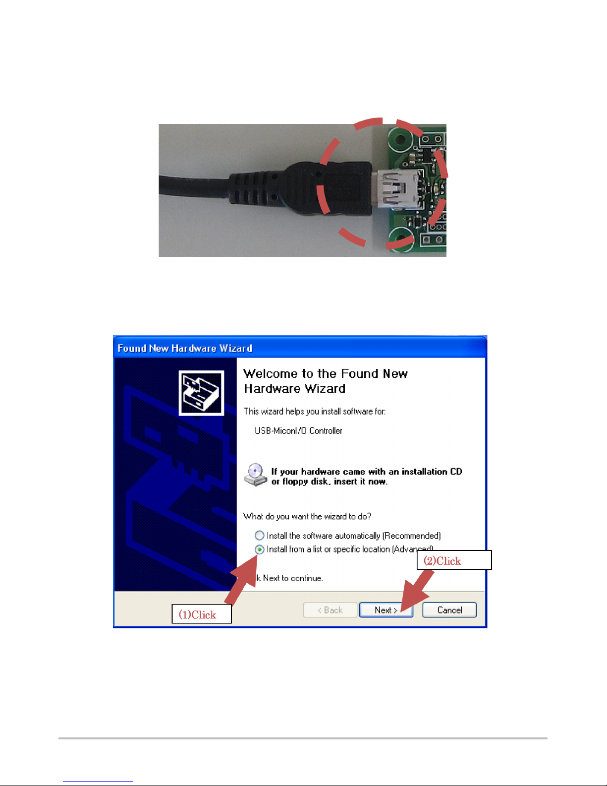
• Connect the PC and this product via USB-Mini cable
Figure 5. Connection via USB-Mini Cable
• After connected, below window appears automatically
• Install the driver in PC (In case of Windows XP 32bit)
Figure 6. Driver Installation − Step 1
http://onsemi.com
6
Page 7

LC87F1MADG1AGEVK
Figure 7. Driver Installation − Step 2
Figure 8. Driver Installation − Step 3
http://onsemi.com
7
Page 8

LC87F1MADG1AGEVK
Figure 9. Driver Installation − Step 4
• LED will light-up if the installation is successful
• Connect the device and the interface cable of this
product
• Start the application named
“LC87F1MADG1AGEVK_Application.exe”
Figure 10. Device Connection
http://onsemi.com
8
Page 9

LC87F1MADG1AGEVK
SPECIFICATION OF THE INPUT/OUTPUT TYPES
I2C Communication
1. Summary:
SIO of LC87F1M16A microcontroller is used for
this communication…
This communication format is based on
2
“THE I
C−BUS SPECIFICATION
VERSION 2.1”
2. Pins to Be Used:
SI: used as SDA of I
CK:used as SCL of I
Table 5. SUMMARY OF THE COMMUNICATION
Address Value Value Next to the Address Value Summary of the Address Value
0b0000 0000 General Call Address
2
C bus
2
C bus
General Call Processing
Value Summary
0x06 Reset of the Slave
0x04 Initialization of the Slave Address
0x00 Do Not Use
0bXXXX XXX1 X are Master Address
3. Summary of the Communication:
• Only Supports Single Master Mode
• Only Supports Fast-mode (Bit Rate is 400 kbps)
• Number of Receivable Data at One
Communication is 0 to 62 Byte (in Case of
10 Bit Address, 61 Byte)
• Number of Transmittable Data at One
Communication is 0 to 62 Byte
• Corresponding Address
0b0000 0001 None Start Byte
0b0000 001X None CBUS Address (No comm.)
0b0000 010X None No Communication
0b0000 011X None No Communication
0b0000 1XXX None No Communication
0b1111 1XXX None No Communication
0b1111 0XXZ Lower 8bit of the Slave Address 10bit Slave Address
Other Transmission Data if Transmission.
Number of Reception Data if Reception.
NOTE: X denotes 0 or 1.
(XX is the Higher 2bit of the Slave Address)
Transmission when Z = 0
Reception When Z = 1
7bit Slave Address
Transmission when Lower1 Bit is 0
Reception when Lower1 Bit is 1
http://onsemi.com
9
Page 10

4. Application Window:
LC87F1MADG1AGEVK
SPI
1. Summary:
SIO of LC87F1M16A microcontroller is used for
this communication…
This communication is based on “SPI Block Guide
V4.01”
2. Pins to Be Used:
SO: used as MOSI of SPI
SI: used as MISO of SPI
Figure 11. Application Window (I2C)
CK: used as SCK of SPI
GPIO:used as SS of SPI
3. Communication Summary:
• Only SupportsNormal Mode
• Bit Rate is 400 kbps
4. Application Window:
Figure 12. Application Window (SPI)
http://onsemi.com
10
Page 11

LC87F1MADG1AGEVK
PWM
1. Summary:
Synchronous×2ch, asynchronous×2ch, total of 4ch
can be output as PWM.
Using filter, it is capable of small DC voltage step
control.
2. Pins to Be Used:
PWM0: Frequency is synchronized with PWM1
(Duty can be set separately)
PWM1: Frequency is synchronized with PWM0
(Duty can be set separately)
PWM2: Frequency and duty can be set
asynchronously.
PWM3: Frequency and duty can be set
asynchronously.
3. Output Summary: PWM0, 1 and PWM2, 3
4. Application Window:
T able 6. PWM0, 1
Frequency Duty Changeable Step
750.0 [kHz] 16 steps
375.0 [kHz] 32 steps
250.0 [kHz] 48 steps
187.5 [kHz] 64 steps
150.0 [kHz] 80 steps
125.0 [kHz] 96 steps
107.1 [kHz] 112 steps
93.8 [kHz] 128 steps
83.3 [kHz] 144 steps
75.0 [kHz] 160 steps
68.2 [kHz] 176 steps
62.5 [kHz] 192 steps
57.7 [kHz] 208 steps
53.6 [kHz] 224 steps
50.0 [kHz] 240 steps
T able 7. PWM2, 3
Frequency Duty Changeable Step
15.625 [kHz] 256 steps
7.813 [kHz] 256 steps
3.906 [kHz] 256 steps
1.953 [kHz] 256 steps
0.977 [kHz] 256 steps
0.488 [kHz] 256 steps
0.244 [kHz] 256 steps
0.122 [kHz] 256 steps
Figure 13. Application Window (PWM)
http://onsemi.com
11
Page 12

Digital Input/Output (GPIO)
1. Summary:
Capable of selecting 3.3 V or 0 V of input/output
2. Pins to Be Used:
GPIO0: Select Low/High when output, and select
Open/Pull-up when input.
GPIO1: Select Low/High when output, and select
Open/Pull-up when input.
GPIO2: Select Low/High when output, and select
Open/Pull-up when input.
GPIO3: Select Low/High when output, and select
Open/Pull-up when input.
GPIO4: Select Low/High when output, and select
Open/Pull-up when input.
GPIO5: Select Low/High when output, and select
Open/Pull-up when input.
GPIO6: Select Low/High when output, and select
Open/Pull-up when input.
GPIO7: Select Low/High when output, and select
Open/Pull-up when input.
GPIO8: Select Low/High when output, and select
Open/Pull-up when input.
GPIO9: Select Low/High when output, and select
Open/Pull-up when input.
GPIO10: Select Low/High when output, and select
Open/Pull-up when input.
GPIO11: Select Low/High when output, and select
LC87F1MADG1AGEVK
Open/Pull-up when input.
GPIO12: Select Low/High when output, and select
Open/Pull-up when input.
GPIO13: Select Low/High when output, and select
Open/Pull-up when input.
GPIO14: Select Low/High when output, and select
Open/Pull-up when input.
GPIO15: Select Low/High when output, and select
Open/Pull-up when input.
GPIO16: Select Low/High when output, and select
Open/Pull-up when input.
GPIO17: Select Low/High when output, and select
Open/Pull-up when input.
GPIO18: Select Low/High when output, and select
Open/Pull-up when input.
GPIO19: Select Low/High when output, and select
Open/Pull-up when input.
GPIO20: Select Low/High when output, and select
Open/Pull-up when input.
3. State of Terminal:
Open input
Input with pull-up
Low output
High output
4. Application Window:
Figure 14. Application Window (GPIO)
http://onsemi.com
12
Page 13

ADC
1. Summary:
Converts the voltage to the value
2. Pins to be used:
GPIO0: ADC port 0
GPIO1: ADC port 1
GPIO2: ADC port 2
GPIO3: ADC port 3
GPIO4: ADC port 4
GPIO5: ADC port 5
GPIO6: ADC port 6
GPIO7: ADC port 7
Note: Set the GPIO to Open when conversion
LC87F1MADG1AGEVK
3. Setting:
− 8bitAD/12bitAD
− Selection of conversion time
8bitAD
Conversion Time
2.8 4.5
5.5 8.8
10.8 17.5
21.5 34.8
42.8 69.5
85.5 138.8
170.8 277.5
341.5 554.8
4. Application Setting Window:
12bitAD
Conversion Time
Unit
ms
ms
ms
ms
ms
ms
ms
ms
Figure 15. Application Setting Window (ADC)
http://onsemi.com
13
Page 14

LC87F1MADG1AGEVK
CIRCUIT DIAGRAM
http://onsemi.com
14
Page 15

LC87F1MADG1AGEVK
PARTS LIST
Table 8. BILL OF MATERIALS
Designator Qty. Description Value Tolerance
C1, C2,
C3
C3, C8,
C20
C6 1 Capacitor SMD
C7 1 Capacitor SMD
C9, C10 2 Capacitor SMD 5 pF, 50 V ±0.25 pF 0402 (1005) Murata GRM1552P1H5R0CZ01# Yes
C11, C12 2 Open NC − − − − −
CF1 1 Ceramic
ZD1 1 Zener Diode 6.2 V, 200 mW SOD−523 ON Semiconductor MM5Z6V2ST1G Yes
D1 1 Diode SOD−323−2 ON Semiconductor MMDL6050T1G Yes
IC1 1 Micro Controller SQFP48
IC2 1 LDO Regulator 3.3 V, 500 mA TSOT23 ON Semiconductor CAT6219−330TDGT3 Yes
LED1 1 LED SMD RED 0603 (1608) STANLEY UR111C Yes
Q1 1 Dual Pch-MOS −30 V, −0.2 A ±5% 0402 (1005) ON Semiconductor MCH6601 Yes
R6 1 Resistor SMD
R1 1 Resistor SMD
R2 1 Resistor SMD
R4, R5 2 Resistor SMD
R3, R9,
R10
R8 1 Resistor SMD
R11, R12 2 Resistor SMD
R13 1 Open NC − − − − −
RD2 1 Resistor SMD
R7 1 Resistor SMD
USB_CN1 1 Connecter USB−B
CN 1, 2, 3 1 Pin Header
3 Capacitor SMD
3 Capacitor SMD
Resonator
3 Resistor SMD
5 × 3
0.1 mF, 10 V
2.2 mF, 10 V
4.7 mF, 16 V
0.01 mF, 10 V
12 Mhz, 33 pF ±0.07% CE Murata CSTCE12M0GH5L Yes
100 kW,
0.063 W
330 kW,
0.063 W
100 W, 0.063 W
33 W, 0.063 W
1.5 kW,
0.063 W
10 kW, 0.063 W
0 W, 0.063 W
330 W, 0.063 W
2.2 kW,
0.063 W
Connector
(MINI)
5 × 3 HIROSUGI PSR−430256−05 Yes
±10% 0402 (1005) Murata GRM155B11A104KA01# Yes
±20% 0603 (1608) Murata GRM188B31A225ME33# Yes
±10% 0805 (2012) Murata GRM21BB31C475KA87L Yes
±10% 0402 (1005) Murata GRM155R61A103KA01# Yes
±5% 0402 (1005) Rohm MCR01MZPJ104 Yes
±5% 0402 (1005) Rohm MCR01MZPJ334 Yes
±5% 0402 (1005) Rohm MCR01MZPJ101 Yes
±5% 0402 (1005) Rohm MCR01MZPJ330 Yes
±5% 0402 (1005) Rohm MCR01MZPJ152 Yes
±5% 0402 (1005) Rohm MCR01MZPJ103 Yes
±5% 0402 (1005) Rohm MCR01MZPJ000 Yes
±5% 0402 (1005) Rohm MCR01MZPJ331 Yes
±5% 0402 (1005) Rohm MCR01MZPJ222 Yes
− − Molex 54819−0519 Yes
Footprint
inch (mm)
(7 × 7)
Manufacturer
ON Semiconductor LC87F1M16AF5ZA0WA−6H No
Manufacturer
Part Number
Substitution
Allowed
Included
Parts
1 Pin Header
Socket 5 × 3
NOTE: All devices are Pb-Free.
5 × 3 HIROSUGI FSS−43085−05 Yes
http://onsemi.com
15
Page 16

LC87F1MADG1AGEVK
PATTERN DIAGRAM − FRONT
http://onsemi.com
16
Page 17

LC87F1MADG1AGEVK
PATTERN DIAGRAM − BACK
http://onsemi.com
17
Page 18

LC87F1MADG1AGEVK
PATTERN DIAGRAM − LOCATION OF THE PARTS
http://onsemi.com
18
Page 19

Application Does Not Start
LC87F1MADG1AGEVK
IF YOU THINK IT IS BROKEN
Check
start.
YES
Check the
LED is lit up.
NO
Check if the driver
is installed.
YES
Remove the USB cable,
devices and everything
connected to this product.
Connect only PC and this
product via USB-mini cable.
NO
NO
Check the device manager that is shows like a
red circle shown above. (In case of Windows XP)
Go back to How to use this
product section, and install.
Start the application.
YES
Start the application.
NO
Check About application
and PC environment.
YES
This product is broken.
OK
NO
Problem solved.
http://onsemi.com
19
Page 20

LC87F1MADG1AGEVK
P
al
ON Semiconductor and are registered trademarks of Semiconductor Components Industries, LLC (SCILLC). SCILLC owns the rights to a number of patents, trademarks,
copyrights, trade secrets, and other intellectual property. A listing of SCILLC’s product/patent coverage may be accessed at www.onsemi.com/site/pdf/Patent−Marking.pdf. SCILLC
reserves the right to m ake c hanges w ithout f urt her n otice t o a ny p roducts h erein. S CILLC m akes n o warrant y, representation or guarantee regar ding t h e s uit ability o f i t s p r oducts f or any
particular purpose, nor does SCILLC assume any liability arising out of the application or use of any product or circuit, and specifically disclaims any and all liability, including without
limitation special, consequent ial o r i ncidental d amages. “ Typical” parameters which may b e p rovided i n S CILLC d ata s heets a nd/or specifications can and do v ary i n d if ferent a pplications
and actual performance may vary over time. All operating parameters, including “Typicals” must be validated for each customer application by customer’s technical experts. SCILLC
does not convey any license under its patent rights nor the r ights of others. SCILLC products are not designed, intended, or authorized for use as components in systems intended for
surgical implant into the b ody, or other applications i ntended t o s upport o r s ustain l ife, o r f or a ny o t her a pplicat ion i n w hich the failure of the SCILLC pr oduct c ould c reate a s ituation w here
personal injury or death may occur. S hould B uyer p urchase o r u se S CILLC p r oduct s for any such unintended or unauthorized application, Buyer shall indemnify and hold SCILLC and
its officers, e mployees, s ubsidiaries, a f filiates, a nd d istributors h armless a gainst all claims, costs, d amages, and expenses, and r easonable a ttorney fees arising out o f, d irectly o r i ndirect ly,
any claim of personal injury or death associated with such unintended or unauthorized use, even if such claim a lleges t hat SCILLC was negligent regarding the design or manufacture
of the part. SCILLC is an Equal Opportunity/Affirmative Action Employer. This literature is subject to all applicable copyright laws and is not for resale in any manner.
UBLICATION ORDERING INFORMATION
LITERATURE FULFILLMENT:
Literature Distribution Center for ON Semiconductor
P.O. Box 5163, Denver, Colorado 80217 USA
Phone: 303−675−2175 or 800−344−3860 Toll Free USA/Canada
Fax: 303−675−2176 or 800−344−3867 Toll Free USA/Canada
Email: orderlit@onsemi.com
N. American Technical Support: 800−282−9855 Toll Free
USA/Canada
Europe, Middle East and Africa Technical Support:
Phone: 421 33 790 2910
Japan Customer Focus Center
Phone: 81−3−5817−1050
http://onsemi.com
20
ON Semiconductor Website: www.onsemi.com
Order Literature: http://www.onsemi.com/orderlit
For additional information, please contact your loc
Sales Representative
EVBUM2170/D
 Loading...