

Page 1
Low Power &
f
High-Resolution Audio
Processing System SoC for
Portable Sound Solution
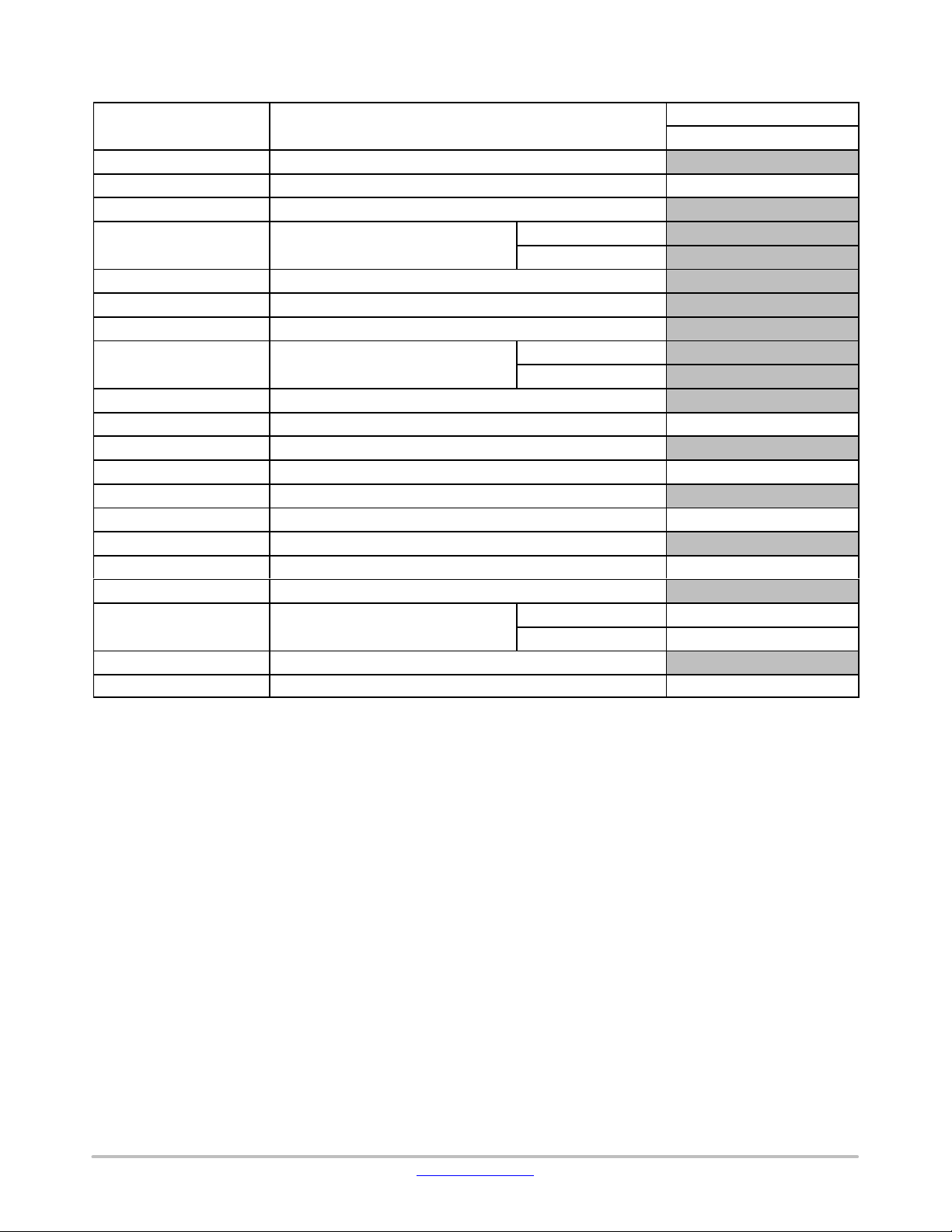
LC823455
Description
LC823455 is an audio processing System−on−Chip (SoC) for
recording and playback, with High−Resolution 32−bit & 192 kHz
audio processing capability that provides the key functions required
for portable audio solutions.
It has a Dual CPU configuration and a DSP providing intensive
processing capability, 4316 KB of internal SRAM that supports the
implementation of large-scale programs for WLAN applications, and
multiple interfaces for increased extensibility. Its features an extensive
range of functions including SBC/AAC codec and Active Noise
Canceller by the DSP, UART and ASRC − applicable for wearable
audio applications. The highly integrated implementation of this rich
set of analog functions results in a miniature footprint with ultra− low
power consumption. This, along with its high performance, makes the
LC823455 suitable for portable audio markets such as Wireless
headsets.
This document describes features, basic functions, electrical
specifications, characteristics, application diagrams and package
dimension of this SoC.
Features
• Ultra Low Power Consumption
®
• Arm
• Proprietary 32−bit DSP Core (LPDSP32)
• Internal Large−Scale Size SRAM : 4316 KB (4 MB + 220 KB)
• High−Resolution 32−bit & 192 kHz Audio Processing Capability
• Several DSP Codes Available for Audio Functions
• Hard−Wired Audio Functions Built−In:
• Analog Blocks Built−in:
• USB2.0 Device with an Integrated PHY, eMMC and SD Card I/F,
Cortex®−M3 Dual Core
MP3 decoder, MP3 encoder,
6 band Equalizer
Synchronous SRC, Asynchronous SRC, etc.
System PLL, Audio PLL,
16−bit DAC, Class−D amp, etc.
Serial Flash I/F(Quad) with Cache Memory,
SPI, UART, I2C, etc.
www.onsemi.com
WLCSP120, 4.086x4.086x0.62
CASE 567WG
LFBGA136, 11.0x11.0
CASE 566GB
ORDERING INFORMATION
See detailed ordering and shipping information on page 104 o
this data sheet.
Typical Applications
• Wearable Earbuds
• Wearable Headphone
• Wireless Speaker
• IC Recorder
© Semiconductor Components Industries, LLC, 2017
April, 2021 − Rev. 3
NOTE:
LC823455RB−2H is under planning.
LC823455RB−2H : Package Code = RB
1 Publication Order Number:
LC823455/D
Page 2

LC823455
Table of Contents
Abstract 3................................................................................................
Terminal Function 21......................................................................................
Pin Assignment 36........................................................................................
Input/Output Circuit 45.....................................................................................
Electrical Specification 55..................................................................................
AC Characteristics 69.....................................................................................
www.onsemi.com
2
Page 3

ABSTRACT
LC823455
Features
• Cortex−M3 Dual Core, AMBA
♦ Internal SRAM (4 M-byte)
♦ Internal ROM (256 k-byte). Boot code, Standard
®
(AHB/APB) system
Functions
♦ DMA Controller (8 ch)
♦ Interrupt Controller (External 90 ch, Internal 83 ch)
♦ SPI (2 ch)
♦ Serial Flash I/F (1 ch)
♦ Quad SPI, cache memory (16 k-byte, 4way set
associative, 128 line) function available
♦ UART (3ch)
UART1, UART2: w/flow control (CTS, RTS)
UART0: w/o flow control
♦ I2C (2ch) Single Master, Full/Standard
♦ GPIO (90 ch)
♦ Pin multiplex function (I2C:2 ch, SPI:2 ch, UAR T:3
ch, MTM:2 ch, DMIC:2 ch x 2)
♦ Plain Timer w/ Watch Dog Timer (1 ch×3)
♦ Multiple Timer (2 ch×4)
♦ 12 bit ADC (8 ch)
♦ SD Card I/F (3 ch)
eSD/eMMC, UHS−I, w/o CPRM
−SD0: eSD/eMMC boot supported (Internal ROM
Boot function)
− SD1: 1.8 V/3.3 V dedicated power supply
− SD2 :
♦ USB2.0 Device (HS/FS) Controller,
Integrated PHY.
Xtal (XT1) is required for USB function, 12, 19.2,
24 MHz for device w/o OTG function.
♦ Real Time Clock
2 modes below are available
− General RTC mode : RTC w/o key input
− KeyInt RTC mode : RTC w/ key input which
enables power on function
♦ SWD (Serial Wire Debug) is supported as the debug
interface
SWV (Serial Wire Viewer) is supported as the trace
interfaceOnly one of Cortex−M3 Dual Core can be
traced
Availability of features explained here depends on
products.
• MP3 hard wired encoder/decoder
♦ MP3 MPEG1, MPEG2, MPEG2.5
− Sampling rate: 8 kHz,11.025 kHz,12 kHz,
16 kHz, 22.05 kHz, 24 kHz, 32 kHz, 44.1 kHz,
48 kHz
− Bit rate: 8 Kbps to 320 Kbps (Decoder−VBR
supported)
• LPDSP32 system
♦ Internal SRAM (220 kbyte)
♦ Audio codec
− MP3
− WMA
− AAC
− SBC
− FLAC, etc.
♦ Audio function
− Active Noise Canceller
− 1−mic/2−mic Noise Canceller for Recorder
− 2−mic Noise Canceller for Hands Free
− Echo Canceller
− Variable Speed Control playback etc.
♦ JTAG ICE
1
MPEG Layer−3 audio coding technology licensed from Fraunhofer IIS and Thomson. Supply of this product does not convey license nor
imply any right to distribute content created with this product in revenue−generating broadcast systems (terrestrial, satellite, cable and/or
other distribution channels), streaming applications (via Internet, intranets and/or networks), other content distribution systems (pay−au-
dio or audio−on−demand applications and the like) or on physical media (compact discs, digital versatile discs, semiconductor chips,
hard drives, memory cards and the like). For details, please visit http://mp3licensing.com/
Supply of this product does not convey license under the relevant intellectual property of Thomson and/or Fraunhofer Gesellschaft nor
imply any right to use this product in any finished end user or ready−to−use final product. An independent license for such use is required.
For details, please visit http://mp3licensing.com/
2
This product contain technology of Microsoft company ownership, and you cannot distribute or use without getting license from Microsoft
Licensing Company.
www.onsemi.com
3
Page 4

LC823455
• Bluetooth Protocol Stack available
• Audio
♦ MP3 hard wired encoder/decoder, MP3 MPEG1,
MPEG2, MPEG2.5
− Sampling rate: 8 kHz,11.025 kHz,12 kHz,16 kHz,
22.05 kHz, 24 kHz, 32 kHz, 44.1 kHz, 48kHz
− Bit rate :8 Kbps to 320 Kbps
(Decoder−VBR supported)
♦ Other audio functions available
− 6 band Equalizer (EQ3)
− Hardware Mixer
− Volume, Mute
− Level Meter
− Audio Timer w/ interrupt generation
− 16/24/32 bit 192 kHz PCM I/F (2ch×2).
Master/slave, I2S
− SSRC (Synchronous Sampling Rate Converter)
0.25 to 64 conversion capable
− ASRC (Asynchronous Sampling Rate Converter)
Jitter reducing function supporting USB audio
class and Bluetooth streaming
− Beep generator
− Digital Microphone I/F (2ch x2), Sampling rate :
up to 48 kHz, Support up to 4 PDM Digital
Microphones
− 16 bit Audio DAC (2 ch)
w/ Class−D Amplifier for Head Phone (2 ch).
Requires external LC LPF
• Audio clock generation
♦ Dedicated PLL for audio
♦ Selectable PLL reference clock
XT1 (12, 19.2, 24 MHz Main xtal)
XTRTC (32.768 kHz RTC xtal)
PCM I/F MCLK0 (/MCLK1), BCK0, BCK1
• Power supply
♦ Typical voltage
− LOGIC(Vdd1),XT1(VddXT1),
PLL1(AVddPLL1), PLL2(AVddPLL2) = 1.0 V
− RTC(VddRTC) = 1.0 V
− I/O(Vdd2) = 1.8 V or 3.3 V
− SD1(VddSD1) = 1.8 V or 3.3 V
− ADC(AVddADC) = 1.8V
− USB PHY(DVddUSBPHY1) = 1.0 V,
(AVddUSBPHY2) = 3.3 V,
(AVddUSBPHY18) = 1.8 V
− Class−D Amplifier
(AVddDAMPL,AVddDAMPR) = 1.5 V
3
The product name for which Bluetooth Protocol Stack is available is determined. Please contact our representative for license fee for the
Stack.
Copyright 1999−2014 OpenSynergy GmbH
All rights reserved. All unpublished rights reserved.
www.onsemi.com
4
Page 5
Package Codes and Functional Differences
Table 1. FUNCTIONAL DIFFERENCES
Package Code
XA
RB
Package
WLP120
BGA136
SDRAM Controller
−
−
External Memory
−
−
SD0
Shared pins with S−Flash function
Dedicated
P−SRAM−−
USB2.0
HS/FS Device
HS/FS Device
12 bit ADC
3ch
8ch
PLL1
Only Internal Loop Filter
Only Internal Loop Filter
XTALINFO[1:0] input
“00”
“00”
RTCMODE input
“0”
Available
BACKUPB input
Connected with VDET internally
Available
KEYINT input
2ch
2ch
External Interrupt
52 ch
53 ch
GPIO
52 ch
53 ch
The product with Package Code = “RB” is under planning.
Function
Controller
PLL2
LC823455
(24 MHz)
(KEYINT RTC mode)
(24 MHz)
www.onsemi.com
5
Page 6
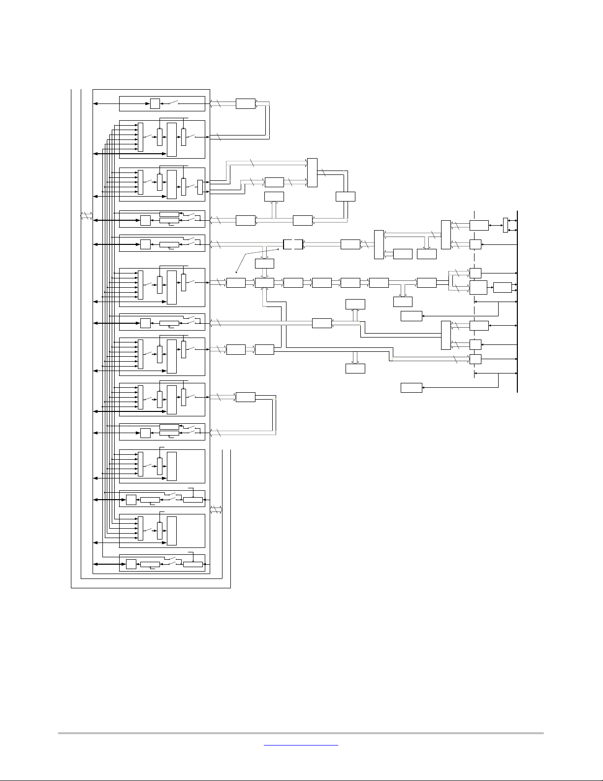
Block Diagram
SWD/SWV
ICE
LC823455
JTAG
ICE
12MHz,
19.2MHz,
32.768kHz
24MHz
XT 1 XTRTC
PSRAM I/F
(1ch
EXT4
SDRAM
CTRL
Controller
USB2.0
Main
Module
Manager
)
Reset
PD -J
(512 byte×3)
BUF
SD I/F
(3ch
ARM Cortex-M3
S-Flash I/F
(1ch)
Cache
(16 Kbyte)
External
Memory
Controller
USB
PHY
Plain
Timer
(1ch×
PD -H
)
PD -G
PD -E
XT1
3)
ARM Cortex-M3
Multilayer Bus
BASIC
BUF
(16 Kbyte)
USB2.0
Device
Multiple
Timer
(2ch×
4)
EXT1
OSC
System
PLL
XT1 RC
XTRTC
EXT3
LPDSP32
APB
Bridge
SRAM S7B
(224Kbyte)
PD -9
SRAM S5A
(384Kbyte)
PD -6
SRAM S1
(256Kbyte)
PD -3
12 bit ADC
(8ch )
PORT0~4
(80 I/O)
DMAC
(8ch)
SRAM S7A
(256Kbyte)
SRAM S4
(256Kbyte)
SRAM S0B
(128Kbyte)
PD -2
SPI
(2ch )
PORT5
(10 I/O)
(1536Kbyte)
PD -5
UART
(3ch )
SRAM S9
(220Kbyte)
PD -10
SRAM S6
PD -8
SRAM S3
(256Kbyte)
SRAM S0A
(128Kbyte)
RTC
SRAM S8
(32Kbyte)
SRAM S5B
(384Kbyte)
PD -7
SRAM S2
(256Kbyte)
PD -4
ROM
(256Kbyte)
PD -1
I2C
(2ch )
MP3
Decoder
16bit Audio
DAC
Class-D
AMP
Audio Buffer
(256 Kbyte)
PCM
I/F
A
N
C
*
Digital
Mic
ATM
BEEP
VOLUME
PCM
I/F
MP3
Encoder
EQ3
METER
MUTE
BCK0/1
MCLK0/1
(PCM I/F)
SSRC
ASRC
Digital
Mic
MIXER
PD -A
Figure 1. T op−Level Block Diagram
www.onsemi.com
6
OSC
Audio PLL
XT1
AHB CLK
(HCLK)
XTRTC
PD -RTC
Page 7
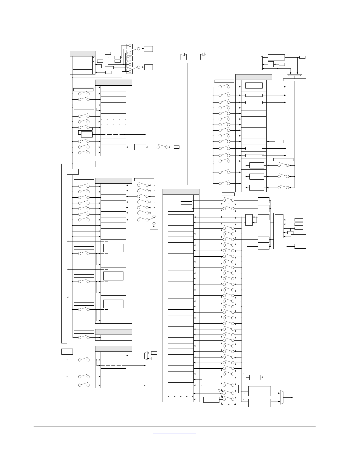
Bus Matrix
LC823455
ARM Cortex−M3
System−Bus
I−Bus
D−Bus
ARM Cortex−M3 LPDSP32
System−Bus
I−Bus
D−Bus
DMIO
DMA
DMB
PM
DMAC
(8ch)
USB2.0
System
ROM
SRAM
(Seg 0)
・・・
SRAM
(Seg 8)
Figure 2. Bus Matrix
SRAM
(Seg 9)
BASIC
Peripheral
EXT1
Peripheral
EXT3
Peripheral
EXT4
Peripheral
APB
Peripheral
www.onsemi.com
7
Page 8
Audio
Internal
Bus
LC823455
256KB SRAM divided into
A
~ N Audio Buffers
by register settings
A buffer
RAM
RAM
Bit conv
RAM
Bit conv
32 Bit conv
Bit conv
RAM
Bit conv
BIT1-0、
BIT1-0、
BIT1-0、
Bit conv
BIT1-0、
Bit conv
MONO
MONO
BIT1-0、
Bit conv
B buffer
D
redirect
E
redirect
G
redirect
J
redirect
L
redirect
N
redirect
C buffer
E
redirect
G
redirect
J
redirect
L
redirect
N
redirect
32
D buffer
RAM
E buffer
RAM Bit conv
F buffer
D
redirect
E
redirect
G
redirect
J
redirect
L
redirect
N
redirect
G buffer
H buffer
D
redirect
E
redirect
G
redirect
J
redirect
L
redirect
N
redirect
I buffer
D
redirect
E
redirect
G
redirect
L
redirect
N
redirect
J buffer
K buffer
D
redirect
E
redirect
G
redirect
J
redirect
N
redirect
L buffer
RAM Bit conv
M buffer
D
redirect
E
redirect
G
redirect
J
redirect
L
redirect
N buffer
RAM Bit conv
RAM Bit conv
RAM Bit conv
BIT1-0、
BIT1-0、
RAM
Bit conv
RAM
Bit conv
32 Bit conv
BIT1-0、
RAM
Bit conv
CBIT1-0、
MONO
BIT1-0、
RAM
Bit conv
CBIT1-0、
MONO
BIT1-0、
BIT1-0、
MONO
CMONO
MONO
CMONO
MONO
BIT1-0、
Bit conv
BIT1-0、
Bit conv
MONO
32 Bit conv
32 Bit conv
MONO
MONO
MONO
MONO
MONO
8
MP3
Encoder
16
24
8
MP3
Decoder
METER
(DEC)
24
VOLUME
(DEC)
32
VOLUME
(AMB)
32
EQ3
32
32
24
DWNMIX
(PS
VOLUME
1)
1)
(PS
ASRC
16
EQ3
DWNMIX
(PS
0
D
E
24
C
S
E
L
1
MUTE
(DEC)
DMCKO0A
SSRC
0
S
I
32
VOLUME
(SP
VOLUME
BTLMIXER
0)
VOLUME
(PS
1)
(SP
0)
0)
METER
(SP
METER
(PS
N
S
E
L
1
MUTE
0)
(PS
1)
SINGEN
METER
(PS
AudioTimer0
METER
0)
(SP
BEEP
0)
LRCK0
1)
LRCK1
AudioTimer1
24
Digtal
1
P
C
32
M
S
E
32
PCM
L
0
SP0
32
PCM
PS0
16 bit
24
Audio
DAC
24
P
C
M
1
S
E
L
Digtal
1
32
PCM
0
SP1
32
PCM
PS1
S
DMDIN0A
E
Mic0
PCM input
PCM output
Mic1
PCM input
PCM output
Class−D
AMP
DMCKO0B
L
DMDIN0B
DIN0
(PCM input)
DOUT0
(PCM output)
LOUT
ROUT
MCLK0/
BCK0/
LRCK0
DMCKO1
DMDIN1
DIN1
(PCM input)
DOUT1
(PCM output)
MCLK1/
BCK1/
LRCK1
24
32
Figure 3. Audio
www.onsemi.com
8
Page 9
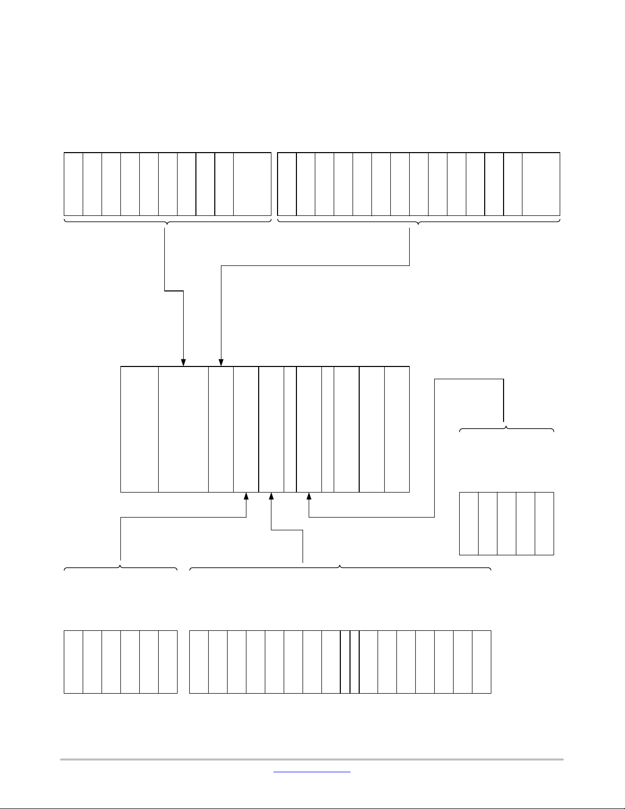
Clock Hierarchy
LC823455
1/(1~64)
1/(1~64)
AHB CLK
(EXT4 only)
Oscillation System
SYSTEM PLL
(PLL1)
1/2、1/4
1/1、1/{(1~63)×2}
BASIC CLK
CORECNT
MCLKCNTBASIC
1/1、1/2、
1/4、1/8
1/(1~64)
AHB CLK(HCLK)
MCLKCNTEXT 1
SDCLK0
MCLKCNTEXT 1
SDCLK1
MCLKCNTEXT 1
SDCLK2
MCLKCNTEXT 1
MCLKCNTEXT 3
MCLKCNTEXT 4
FCLKCNT
XT1
1/4
XTRTC
RC
BASIC
M3Core0
M3Core1
LPDSP32
SRAM/ROM
INTC
DMAC
Cache
S-Flash I/F
External Memory
Controller(XMC)
USB2.0 Device
APB CLK (PCLK )
AHB EXT1
Plain Timer 0
Plain Timer 1
Plain Timer 2
Multiple Timer 0
Multiple Timer 1
Multiple Timer 2
Multiple Timer 3
Audio PLL
System PLL
OSC System
1/1、1/2、1/4、1/8、
1/16、1/32、1/64、
1/128 、1/256 、1/512
SD0(Main Function)
SD0(Card Detect)
1/1、1/2、1/4、1/8、
1/16、1/32、1/64、
1/128 、1/256 、1/512
SD1(Main Function)
SD1(Card Detect)
1/1、1/2、1/4、1/8、
1/16、1/32、1/64、
1/128 、1/256 、1/512
SD2(Main Function)
SD2(Card Detect)
AHB EXT3
AUDIO BUFFER
AHB EXT4
PSRAM I/F
SDRAM CTRL
PHI1 pin
・・・
・・・
1/4
1/2
PHI0 pin
[Note]
- M3Core 0, M3Core 1 and LPDSP 32 has additional clock gating
switch enabled by the execution of a dedicated operation.
SFCK
USB PHY
MCLKCNTEXT 1
XTRTC
PLL1
PSM_SCK
SDRCLK
Figure 4. Clock Hierarchy
12MHz
19.2MHz
24MHz
XT1
(XIN1/XOUT 1 pin)
32.768kHz
XTRTC
(XIN32K/XOUT 32K pin )
MCLKCNTAPB
APB
ADC
1/2、1/4、1/8、
1/16、1/32、1/64
SPI0
1/{(2~256 )×4}
SPI1
1/{(2~256 )×4}
1/1、1/2、1/4、
1/8、1/16
1/4
ADCCLK
(Internal)
PLL1
XT1
1/{(1~8) + (0~63)/64}
SCK0
SCK1
PORT 0
PORT 1
PORT 2
PORT 3
PORT 4
PORT 5
1/2、1/4、
1/8
1/4、1/8、
1/16
1/1、1/2、
1/4
1/1、1/2、
1/4、1/8
1/1、1/2、
1/4、1/8
XTRTC
SCL0
SCL1
MCLKCNTAPB
AUDIO
PLL
(PLL2)
1/4
MCLK 0/MCLK 1
BCK0
BCK1
XT1
(input)
AHB CLK
(HCLK )
XT1
AUDIO Block
MP3DEC
MP3ENC
AUDIO Control
VOLUME DEC
MIXER
EQ3
BEEP
SSRC
ASRC
1/2
1/1、1/2、
1/4
CLOCKEN
FS384
FS192
FS256
RTC
I2C0
1/{(2~65535)×8}
I2C1
1/{(2~65535)×8}
UART0
1/{(8~16)×
(1~65536)}
UART1
1/{(8~16)×
(1~65536)}
UART2
1/{(8~16)×
(1~65536)}
DECCLK
ENCCLK
AUDCLK
1/3
1/2
FS384
SSRCFCLK
ASRCFCLK
FS768
VOLUME SP 0
VOLUME PS0
VOLUME SP 1
VOLUME PS1
VOLUME AMB
METER DEC
METER SP0
METER PS0
METER SP1
METER PS1
[Note]
- Regarding the initial value of switches described in this figure,
refer to the appropriate documents.
- Regarding the frequency of SSRCFCLK and ASRCFCLK,
refer to the SSRC and ASRC Programmer’s Model documents.
- ENCCLK frequency should be192 * FS
while FS is Sampling Frequency of MPEG1 mode of MP3.
ex.) ENCCLK should be8.4672MHz to make all of MP 3 data
44.1/22.05/11.025 KHz (MPEG1/MPEG2/MPEG2.5).
- DECCLK frequency should be384 * FS
while FS is Sampling Frequency of MPEG1 mode of MP3.
ex.) DECCLK should be16.9344MHz to make all of MP 3 data
44.1/22.05/11.025 KHz (MPEG1/MPEG2/MPEG2.5).
MUTE DEC
MUTE PS0
PCMPS0
PCMSP0
PCMPS1
PCMSP1
AudioTimer 0
AudioTimer 1
XT1
SINGEN
DigitalMIC0
DigitalMIC1
PCKGEN
Damp CTL
Class -D AMP
16bit Audio
DAC(Noise Shaping )
DAC(Main)
FCEDAC
1/1, 1/2, 1/4
1/8, 1/16
[Note]
- Class-D AMP has additional clock source and gating switch
for being used as GPO.
1/1, 1/2,
1/4
1/1, 1/2, 1/4, 1/8,
1/1, 1/21/4, 1/8,
1/16, 1/32
1/16, 1/32
FS384
MCLK0/MCLK1
(output )
www.onsemi.com
9
Page 10
Memory Map
All Areas (Cortex−M3)
0x4000 1000
0x4000 0000
0x4000 2000
0x4000 3000
0x4000 4000
0x4000 5000
0x4000 6000
0x4000 7000
0x4001 0000
0x4002 0000
LC823455
0x4004 0000
0x4003 FFFF
0x4004 1000
0x4004 2000
0x4004 3000
0x4004 4000
0x4004 5000
0x4004 6000
0x4004 7000
0x4004 A000
0x4004 9000
0x4004 8000
0x4004 B000
0x4004 C000
0x4004 D000
0x4005 FFFF
S-Flash I/F
MEM CTL
External
USB2.0 CTL
INTC
0x0000 0000
external memory
MUTEX REG
DSP CMDIF
DMAC
peripherals
BASIC
0x4000 0000
SRAM memories
BASIC peripherals
USB2.0 FIFO
reserved
0x4004 0000
0x4006 0000
AHB EXT1 peripherals
reserved
0x4008 0000
AHB EXT3 peripherals
APB peripherals
System
OSC
0x400A 0000
0x6000 0000
reserved
System PLL
Audio PLL
Timer0
0x6402 0000
0xE000 0000
AHB EXT4 peripherals
reserved
Multiple
Multiple
Timer1
0xE004 0000
Private peripheral bus - External
Private peripheral bus - Internal
Multiple
Timer2
0xE010 0000
Multiple
Timer3
Timer0
peripherals
System
Timer1
Plain
AHB EXT1
Timer2
Plain
Plain
0x6000 0000
SD1
SD0
0x6400 0000
0x6200 0000
SD2
peripherals
AHB EXT4
0x6400 2000
0x6400 1000
reserved
0x6401 FFFF
0x4006 1000
0x4006 0000
0x4006 2000
Audio Buffer
Functions
Audio
peripherals
AHB EXT3
0x4006 3000
MP3 Decoder
MP3 Encoder
0x4007 FFFF
0x4006 5000
0x4006 4000
Controles
reserved
Audio
0x4008 1000
System
PORT0
0x4008 2000
0x4008 0000
Controller
peripherals
APB
0x4008 3000
0x4008 4000
0x4008 5000
0x4008 6000
0x4008 7000
0x4008 8000
0x4008 8800
PORT3
PORT4
PORT1
PORT2
PORT5
ADC
SPI0
SPI1
Figure 5. All Areas (Cortex−M3)
www.onsemi.com
10
0x4008 9000
0x4008 A000
I2C0
I2C1
0x4008 B000
0x4008 C000
UART0
UART1
Memory Area
SDRAM
0x4008 D000
0x4008 E000
0x4008 F000
UART2
RTC
SDRAM CTRL
reserved
0x4009 FFFF
reserved
PSRAM I/F
reserved
Page 11
Code Area (Cortex−M3)
Table 2. CODE AREA (CORTEX−M3) − UNREMAPPED (AFTER RESET)
Cortex−M3−0
Cortex−M3−1
System−
I−Bus
D−Bus
System−
I−Bus
D−Bus
0x1C00
Reserved
0x1A00
External memory 1
0x1800
External memory 0
0x0600
Reserved
0x0500
S−Flash I/F
0x0254
Reserved
0x0250
256 KB Internal ROM
0x0243
Reserved
0x0240
220 KB Internal SRAM
0x023F
32 KB Internal SRAM
0x023C
224 KB
0x0238
256KB
0x0220
1536 KB Internal SRAM
0x021A
384 KB
0x0214
384 KB
0x0210
256 KB Internal SRAM
0x020C
256 KB Internal SRAM
0x0208
256 KB Internal SRAM
0x0204
256 KB Internal SRAM
0x0202
128 KB
0x0200
128 KB
0x0004
Reserved
0x0000
256 KB Internal ROM
LC823455
Address Master / Slave
0000
0000
0000
0000
0000
0000
0000
7000
0000
8000
0000
0000
0000
0000
0000
0000
0000
0000
0000
0000
0000
(Memory, Cache)
(seg 9)
(seg 8)
480 KB
Internal
SRAM
(seg 7)
(seg 6)
768 KB
Internal
SRAM
(seg 5)
(seg 4)
(seg 3)
(seg 2)
(seg 1)
256 KB
Internal
SRAM
(seg 0)
(seg 7−B)
(seg 7−A)
(seg 5−B)
(seg 5−A)
(seg 0−B)
(seg 0−A)
Bus
Bus
d d
d d
d d
d d
d d
d d
d d
d d
d d
d d
d d
d d
d d
d d
d d
d d
d d
DMAC USB20
0000
0000
Shadow Area
www.onsemi.com
d d
11
Page 12
LC823455
Table 3. CODE AREA (CORTEX−M3) − REMAPPED (REMAP[1:0]=2’B01)
Cortex−M3−0
Cortex−M3−1
System−
I−Bus
D−Bus
System−
I−Bus
D−Bus
0x1C00
Reserved
0x1A00
External memory 1
0x1800
External memory 0
0x0600
Reserved
0x0500
S−Flash I/F
0x0254
Reserved
0x0250
256 KB Internal ROM
0x0243
Reserved
0x0240
220 KB Internal SRAM
0x023F
32 KB Internal SRAM
0x023C
224 KB
0x0238
256 KB
0x0220
1536 KB Internal SRAM
0x021A
384 KB
0x0214
384 KB
0x0210
256 KB Internal SRAM
0x020C
256 KB Internal SRAM
0x0208
256 KB Internal SRAM
0x0204
256 KB Internal SRAM
0x0202
128 KB
0x0200
128 KB
0x0004
Reserved
0x0002
128 KB
0x0000
128 KB
Address Master / Slave
0000
0000
0000
0000
0000
0000
0000
7000
0000
8000
0000
0000
(Memory, Cache)
(seg 9)
(seg 8)
480 KB
Internal
SRAM
(seg 7)
(seg 7−B)
(seg 7−A)
Bus
Bus
d d
d d
d d
d d
d d
d d
d d
d d
DMAC USB20
0000
0000
0000
0000
0000
0000
0000
0000
0000
0000
0000
0000
768 KB
Internal
SRAM
(seg 5)
256 KB
Internal
SRAM
(seg 0)
256 KB
Internal
SRAM
(seg 0)
Shadow
Area
(seg 6)
(seg 4)
(seg 3)
(seg 2)
(seg 1)
(seg 5−B)
(seg 5−A)
(seg 0−B)
(seg 0−A)
(seg 0−B)
(seg 0−A)
d d
d d
d d
d d
d d
d d
d d
d d
d d
d d
d d
www.onsemi.com
12
Page 13
LC823455
Table 4. CODE AREA (CORTEX−M3) − REMAPPED (REMAP[1:0]=2’B11)
Cortex−M3−0
Cortex−M3−1
System−
I−Bus
D−Bus
System−
I−Bus
D−Bus
0x1C00
Reserved
0x1A00
External memory 1
0x1800
External memory 0
0x0600
Reserved
0x0500
S−Flash I/F
0x0254
Reserved
0x0250
256 KB Internal ROM
0x0243
Reserved
0x0240
220 KB Internal SRAM
0x023F
32 KB Internal SRAM
0x023C
224 KB
0x0238
256 KB
0x0220
1536KB Internal SRAM
0x021A
384 KB
0x0214
384 KB
0x0210
256KB Internal SRAM
0x020C
256KB Internal SRAM
0x0208
256KB Internal SRAM
0x0204
256KB Internal SRAM
0x0202
128 KB
0x0200
128 KB
0x0000
External memory 0
Address Master / Slave
0000
0000
0000
0000
0000
0000
0000
7000
0000
8000
0000
0000
(Memory, Cache)
(seg 9)
(seg 8)
480 KB
Internal
SRAM
(seg 7)
(seg 7−B)
(seg 7−A)
Bus
Bus
d d
d d
d d
d d
d d
d d
d d
d d
DMAC USB20
0000
0000
0000
0000
0000
0000
0000
0000
0000
0000
768 KB
Internal
SRAM
(seg 5)
256 KB
Internal
SRAM
(seg 0)
Shadow Area
(seg 6)
(seg 4)
(seg 3)
(seg 2)
(seg 1)
(seg 5−B)
(seg 5−A)
(seg 0−B)
(seg 0−A)
d d
d d
d d
d d
d d
d d
d d
d d
d d
d d
www.onsemi.com
13
Page 14
SRAM Area (Cortex−M3)
Table 5. SRAM AREA (CORTEX−M3)
Cortex−M3−0
Cortex−M3−1
System−
I−Bus
D−Bus
System−
I−Bus
D−Bus
0x2600
Reserved
0x2500
S−Flash I/F
0x2400
S−Flash I/F
0x2043
Reserved
0x2040
220 KB Internal SRAM
0x203F
32 KB Internal SRAM
0x203C
224 KB
0x2038
256 KB
0x2020
1536 KB Internal SRAM
0x201A
384 KB
0x2014
384 KB
0x2010
256 KB Internal SRAM
0x200C
256 KB Internal SRAM
0x2008
256 KB Internal SRAM
0x2004
256 KB Internal SRAM
0x2002
128 KB
0x2000
128 KB
LC823455
Address Master / Slave
0000
0000
0000
7000
0000
8000
0000
0000
0000
0000
0000
(Memory, Cache)
(Memory, No Cache)
(seg 9) Shadow area
(seg 8) Shadow area
480 KB
Internal
SRAM
(seg 7)
Shadow
area
(seg 6) Shadow area
768 KB
Internal
SRAM
(seg 5)
Shadow
area
(seg 7−B)
(seg 7−A)
(seg 5−B)
(seg 5−A)
Bus
d d d
d d d
d d d
d d d
d d d
d d d
d d d
d d d
d d d
Bus
DMAC USB20
0000
0000
0000
0000
0000
0000
(seg 4) Shadow area
(seg 3) Shadow area
(seg 2) Shadow area
(seg 1) Shadow area
256 KB
Internal
SRAM
(seg 0)
Shadow
area
(seg 0−B)
(seg 0−A)
d d d
d d d
d d d
d d d
d d d
d d d
www.onsemi.com
14
Page 15
Other Areas (Cortex−M3)
Table 6. OTHER AREAs (CORTEX−M3)
Cortex−M3−0
Cortex−M3−1
System−
I−Bus
D−Bus
System−
I−Bus
D−Bus
0xE010
Reserved
0xE00F
ROM table
0xE00F
CORE REG
0xE004
Reserved
0xE004
TPIU
0xE000
Reserved
0xE000
NVIC
0xE000
Reserved
0xE000
FPB
0xE000
DWT
0xE000
ITM
0x6400
Reserved
0x6400
PSRAM I/F
0x6400
SDRAM CTRL
0x6200
Reserved
0x6000
SDRAM Memory area
0x4008
Reserved
0x4008
RTC
0x4008
UART2
0x4008
UART1
0x4008
UART0
0x4008
I2C1
0x4008
I2C0
0x4008
SPI1
0x4008
SPI0
0x4008
ADC
LC823455
Address Master / Slave
0000
F000
E000
1000
0000
F000
E000
3000
2000
1000
0000
2000
1000
0000
Bus
d
(Note 1)
d
(Note 1)
d
(Note 1)
d
(Note 1)
d
(Note 1)
d
(Note 1)
d
(Note 1)
d d d
d d
Bus
d
(Note 1)
d
(Note 1)
d
(Note 1)
d
(Note 1)
d
(Note 1)
d
(Note 1)
d
(Note 1)
DMAC USB20
0000
0000
F000
E000
D000
C000
B000
A000
9000
8800
8000
7000
d d d
d d
d d d
d d d
d d d
d d
d d
d d d
d d d
d d d
www.onsemi.com
15
Page 16
LC823455
0x4008
PORT5
0x4008
PORT4
0x4008
PORT3
0x4008
PORT2
0x4008
PORT1
0x4008
PORT0
0x4008
System Controller
0x4006
Reserved
0x4006
Audio Controls
0x4006
MP3 Encoder
0x4006
MP3 Decoder
0x4006
Audio Functions
0x4006
Audio Buffer
0x4004
Reserved
0x4004
SD2
0x4004
SD1
0x4004
SD0
0x4004
Plain Timer2
0x4004
Plain Timer1
0x4004
Plain Timer0
0x4004
Multiple Timer3
0x4004
Multiple Timer2
0x4004
Multiple Timer1
0x4004
Multiple Timer0
0x4004
Audio PLL
0x4004
System PLL
0x4004
OSC System
Table 6. OTHER AREAs (CORTEX−M3) (continued)
Cortex−M3−1Cortex−M3−0
System−
Address USB20DMAC
6000
5000
4000
3000
2000
1000
0000
5000
4000
3000
2000
1000
0000
Master / Slave
Bus
d d
d d
d d
d d
d d
d d
d d
d d
d d
d d
d d
d d d
D−BusI−Bus
System−
Bus
D−BusI−Bus
D000
C000
B000
A000
9000
8000
7000
6000
5000
4000
3000
2000
1000
0000
d d d
d d d
d d d
d d
d d
d d
d d
d d
d d
d d
d d
d d
d d
www.onsemi.com
16
Page 17
LC823455
0x4002
Reserved
0x4001
USB2.0 FIFO
0x4000
Reserved
0x4000
DSP CMDIF
0x4000
MUTEX REG
0x4000
DMAC
0x4000
INTC
0x4000
USB2.0 CTL
0x4000
S−Flash I/F
0x4000
External MEM CTL
Table 6. OTHER AREAs (CORTEX−M3) (continued)
Cortex−M3−1Cortex−M3−0
System−
Address USB20DMAC
0000
0000
7000
6000
5000
4000
3000
2000
1000
0000
1. Access from internal peripheral bus(AHB/APB)
Master / Slave
Bus
d d
d d
d d
d d
d d
d d
d d
d d
D−BusI−Bus
System−
Bus
D−BusI−Bus
www.onsemi.com
17
Page 18
LPDSP32
Table 7. LPDSP32 − DMA
LPDSP32
DMA
0x40 0000
Reserved
0x3F 8000
32 KB Internal SRAM (seg 8)
0x3C 0000
224 KB (seg 7−B)
0x38 0000
256 KB (seg 7−A)
0x20 0000
1536 KB Internal SRAM (seg 6)
0x1A 0000
384 KB (seg 5−B)
0x14 0000
384 KB (seg 5−A)
0x10 0000
256 KB Internal SRAM (seg 4)
0x0C 0000
256 KB Internal SRAM (seg 3)
0x08 0000
256 KB Internal SRAM (seg 2)
0x04 0000
256 KB Internal SRAM (seg 1)
0x02 0000
128 KB (seg 0−B)
0x00 0000
128 KB (seg 0−A)
Table 8. LPDSP32 – DMB
LPDSP32
DMB
0xC0 0000
Reserved
0xBF 8000
32 KB Internal SRAM (seg 8)
0xBC 0000
224 KB (seg 7−B)
0xB8 0000
256 KB (seg 7−A)
0xA0 0000
1536 KB Internal SRAM (seg 6)
0x9A 0000
384 KB (seg 5−B)
0x94 0000
384 KB (seg 5−A)
0x90 0000
256 KB Internal SRAM (seg 4)
0x8C 0000
256 KB Internal SRAM (seg 3)
0x88 0000
256 KB Internal SRAM (seg 2)
0x84 0000
256 KB Internal SRAM (seg 1)
0x82 0000
128 KB (seg 0−B)
0x80 0000
128 KB (seg 0−A)
LC823455
Address Master / Slave
480 KB Internal SRAM (seg 7)
768 KB Internal SRAM (seg 5)
256 KB Internal SRAM (seg 0)
d
d
d
d
d
d
d
d
d
d
d
d
Address Master / Slave
480 KB Internal SRAM (seg 7)
768 KB Internal SRAM (seg 5)
256 KB Internal SRAM (seg 0)
d
d
d
d
d
d
d
d
d
d
d
d
www.onsemi.com
18
Page 19
LC823455
Table 9. LPDSP32 − DMIO
LPDSP32
DMIO
0xF0 2000
Reserved
0xF0 1000
PSRAM I/F
0xF0 0000
SDRAM CTRL
0xD0 0000
SDRAM Memory Area
0xC6 5000
Reserved
0xC6 4000
Audio Controls
0xC6 3000
MP3 Encoder
0xC6 2000
MP3 Decoder
0xC6 1000
Audio Functions
0xC6 0000
Audio Buffer
0xC4 A000
Reserved
0xC4 9000
Plain Timer2
0xC4 8000
Plain Timer1
0xC4 7000
Plain Timer0
0xC4 6000
Multiple Timer3
0xC4 5000
Multiple Timer2
0xC4 4000
Multiple Timer1
0xC4 3000
Multiple Timer0
0xC4 2000
Audio PLL
0xC4 1000
System PLL
0xC4 0000
OSC System
0xC0 7000
Reserved
0xC0 6000
DSP CMDIF
0xC0 5000
MUTEX REG
0xC0 4000
DMAC
0xC0 3000
INTC
0xC0 0000
Reserved
Address Master / Slave
d
d
d
d
d
d
d
d
d
d
d
d
d
d
d
d
d
d
d
d
d
d
www.onsemi.com
19
Page 20
LC823455
Table 10. LPDSP32 − PM
LPDSP32
PM
0x50 3332
Reserved
0x50 0000
32 KB Internal SRAM (seg 8)
0x4B 0000
Reserved
224 KB (seg 7−B)
256 KB (seg 7−A)
0x41 9998
Reserved
0x38 0000
1536 KB Internal SRAM (seg 6)
0x34 CCCC
Reserved
384 KB (seg 5−B)
384 KB (seg 5−A)
0x29 9998
Reserved
0x28 0000
256 KB Internal SRAM (seg 4)
0x21 9998
Reserved
0x20 0000
256 KB Internal SRAM (seg 3)
0x19 9998
Reserved
0x18 0000
256 KB Internal SRAM (seg 2)
0x11 9998
Reserved
0x10 0000
256 KB Internal SRAM (seg 1)
0x09 9998
Reserved
128 KB (seg 0−B)
128 KB (seg 0−A)
0x01 6000
Reserved
0x00 0000
220 KB Internal SRAM (seg 9)
Address Master / Slave
0x48 0000 480 KB Internal SRAM (seg 7)
0x30 0000 768 KB Internal SRAM (seg 5)
d
d
d
0x08 0000 256 KB Internal SRAM (seg 0)
2. PM of LPDSP32 cannot access internal SRAM seg5, 6, and 7.
d
d
d
d
d
www.onsemi.com
20
Page 21
LC823455
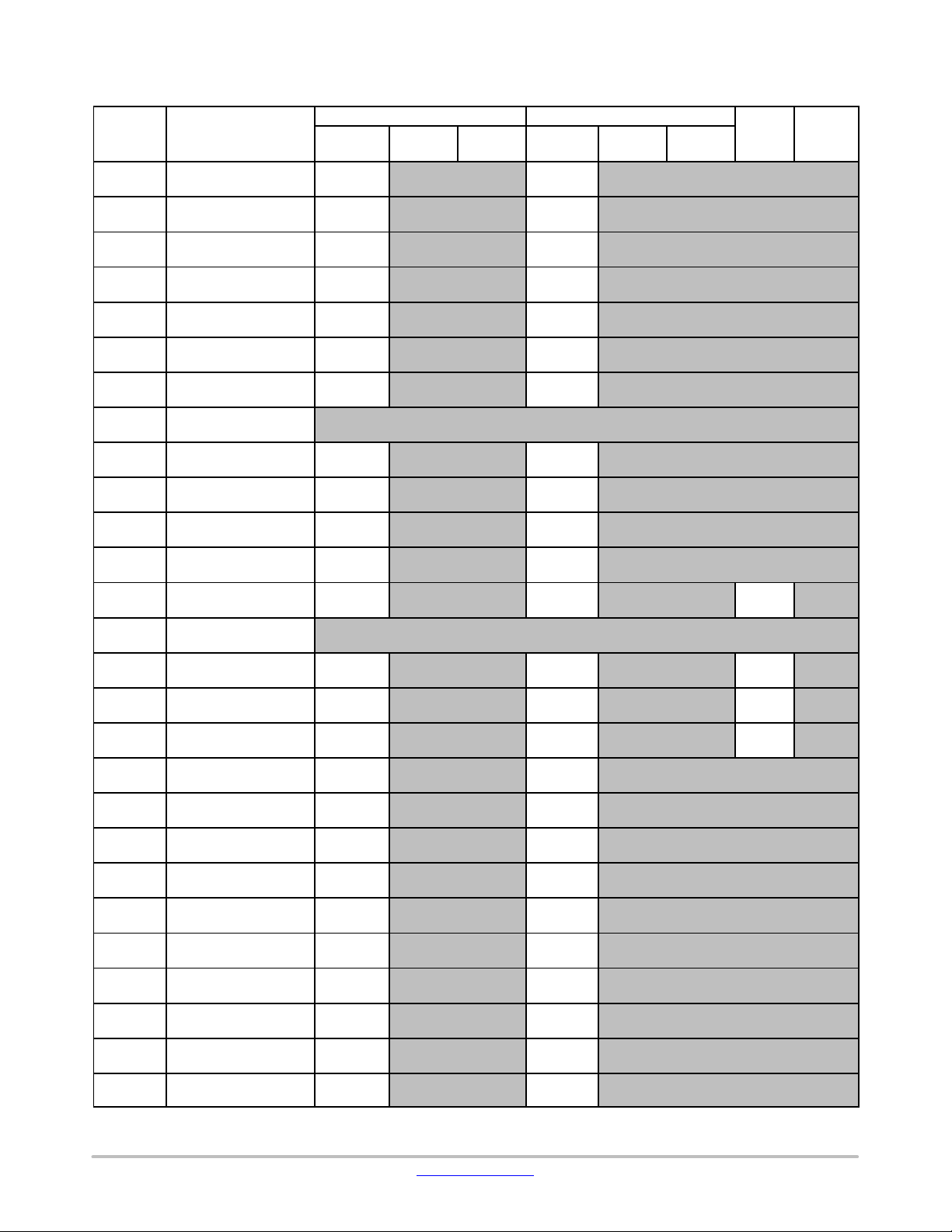
Table 11. TERMINAL FUNCTIONS
Terminal Name
Polarity
Direction
Function
Available(d)
Multiplexed
XA
RB
JTAG/SWD
TDO
−OJTAG test data output
SDWP1
Pos
I
SD I/F Ch1 write protect
GPIO21
−BGPIO
EXTINT21
−IExternal Interrupt 2−bit1
TDI
−IJTAG test data input
SDCD1
Neg
I
SD I/F Ch1 detect
SWO
−Oserial wire view data
GPIO20
−BGPIO
EXTINT20
−IExternal Interrupt 2−bit0
TMS
−IJTAG test data select
SDWP2
Pos
I
SD I/F Ch2 write protect
GPIO28
−BGPIO
EXTINT28
−IExternal Interrupt 2−bit8
TCK
Pos
I
JTAG test clock
SDCD2
Neg
I
SD I/F Ch2 detect
GPIO29
−BGPIO
EXTINT29
−IExternal Interrupt 2−bit9
SWDCLK
Pos
I
Serial wire clock
DMCKO0B
−ODigital Mic Ch0 Clock B Output
GPIO58
−BGPIO
EXTINT58
−IExternal Interrupt 5−bit8
SWDIO
−BSerial wire Data
DMDIN0B
−IDigital Mic Ch0 Data B Input
GPIO59
−BGPIO
EXTINT59
−IExternal Interrupt 5−bit9
Sum
6
6
RTC
XIN32K
Pos
I
32.768KHz XTAL Input (XTRTC)
VddRTC
XOUT32K
−O32.768KHzXTAL Output (XTRTC)
VddRTC
VDET
Neg
I
RTC power detect Input
VddRTC
RTCINT
Neg
O
RTC Interrupt Output (Normal: Hiz, Inter-
VddRTC
BACKUPB
Neg
I
RTC backup mode input
VddRTC
KEYINT[2]
−IRTC KEY input can be used when KeyInt
VddRTC
KEYINT[1:0]
−IRTC KEY input can be used when KeyInt
VddRTC
TERMINAL FUNCTIONS
XA: Package Code = “XA”, RB: Package Code = “RB”, (RB is under planning).
Function
IO POWER
VddSD1
VddSD1
Vdd2
Vdd2
Vdd2
Vdd2
d d
d d
d d
d d
d d
d d
d d
d d
d d
d d
d d
d d
d d
d d
d d
d d
d d
d d
d d
d d
d d
d d
d d
d d
d d
d d
d d
d d
d d
rupt enabled:Low Output)
d
Bonded with VDET internally for “XA”
RTC mode
d d
RTC mode
www.onsemi.com
21
Page 22
Table 11. TERMINAL FUNCTIONS
Terminal Name
RTCMODE
−IRTC mode input (Note 3)
VddRTC
VddRTC
−PRTC power supply
VssRTC
−PRTC ground
Sum
8
10
EXTERNAL INTERRUPT/GPIO
SDRADDR12
−OSDRAM address
GPIO2A
−BGPIO
EXTINT2A
−IExternal Interrupt 2−bit10
SCL1
−OI2C ch1 Clock (open drain output )
GPIO2B
−BGPIO
EXTINT2B
−IExternal Interrupt 2−bit11
SDA1
−BI2C ch1 Data (open drain output )
GPIO2C
−BGPIO
EXTINT2C
−IExternal Interrupt 2−bit12
SDRADDR11
−OSDRAM address
DMCKO0A
−ODigital Mic Ch0 Clock A Output
GPIO2D
−BGPIO
EXTINT2D
−IExternal Interrupt 2−bit13
EXTINT2E
−IExternal Interrupt 2−bit14
GPIO2E
−BGPIO
EXTINT2F
−IExternal Interrupt 2−bit15
GPIO2F
−BGPIO
Sum
5
5
SPI (SERIAL I/F CH0)
SCK0
Neg
B
Serial I/F Ch0 Clock
GPIO1D
−BGPIO
EXTINT1D
−IExternal Interrupt 1−bit13
SDI0
−ISerial I/F Ch0 Data Input
GPIO1E
−BGPIO
EXTINT1E
−IExternal Interrupt 1−bit14
SDO0
−OSerial I/F Ch0 Data Output
GPIO1F
−BGPIO
EXTINT1F
−IExternal Interrupt 1−bit15
Sum
3
3
S−FLASH I/F / SD I/F CH0 (Note 4)
SFCK
Neg
O
Serial Flash I/F Clock
Multiplexed
Function
RTC
(continued)
Set General or KeyInt RTC mode
RTCMODE =
“0” : KeyInt RTC mode
“1” : General RTC mode
Bonded to “0” internally for “XA”
LC823455
FunctionDirectionPolarity
Available(d)
IO POWER
d d d
d d d
Vdd2
RBXA
d
* During Internal ROM boot, this terminal
is used as the boot monitor signal.
Vdd2
Vdd2
Vdd2
Vdd2
Vdd2
Vdd2
Vdd2
Vdd2
d d
d d
d d
d d
d d
d d
d d
d d
d d
d d
d d
d d
d d
d d
d d
d d
d d
d d
d d
d d
d d
d d
d d
(QSPI Clock)
www.onsemi.com
22
Vdd2
d d
Page 23
Table 11. TERMINAL FUNCTIONS
Terminal Name
GPIO0D
−BGPIO
EXTINT0D
−IExternal Interrupt 0−bit13
SDCLK0
−OSD I/F Ch0 Clock Output
SFDI(QIO0)
−
I(B)
Serial Flash I/F Data input
GPIO0E
−BGPIO
EXTINT0E
−IExternal Interrupt 0−bit14
SDAT00
−BSD I/F Ch0 Data0
SFDO(QIO1)
−
O(B)
Serial Flash I/F Data output
GPIO0F
−BGPIO
EXTINT0F
−IExternal Interrupt 0−bit15
SDAT01
−BSD I/F Ch0 Data1
SFWP(QIO2)
Neg
O(B)
Serial Flash I/F write protect
GPIO11
−BGPIO
EXTINT11
−IExternal Interrupt 1−bit1
SDAT02
−BSD I/F Ch0 Data2
SFHOLD(QIO3)
Neg
O(B)
Serial Flash I/F hold
GPIO12
−BGPIO
EXTINT12
−IExternal Interrupt 1−bit2
SDAT03
−BSD I/F Ch0 Data3
Sum
5
5
I2C
SCL0
−OI2C ch0 Clock (open drain output )
GPIO07
−BGPIO
EXTINT07
−IExternal Interrupt 0−bit7
SDA0
−BI2C ch0 Data (open drain output )
GPIO08
−BGPIO
EXTINT08
−IExternal Interrupt 0−bit8
Sum
2
2
Multiplexed
Function
S−FLASH I/F / SD I/F CH0 (Note 4)
(continued)
(QSPI Data 0)
(QSPI Data 1)
(QSPI Data 2)
(QSPI Data 3)
LC823455
FunctionDirectionPolarity
IO POWER
Vdd2
Vdd2
Vdd2
Vdd2
Available(d)
RBXA
d d
d d
d d
d d
d d
d d
d d
d d
d d
d d
d d
d d
d d
d d
d d
d d
d d
d d
d d
www.onsemi.com
23
Vdd2
Vdd2
d d
d d
d d
d d
d d
d d
Page 24
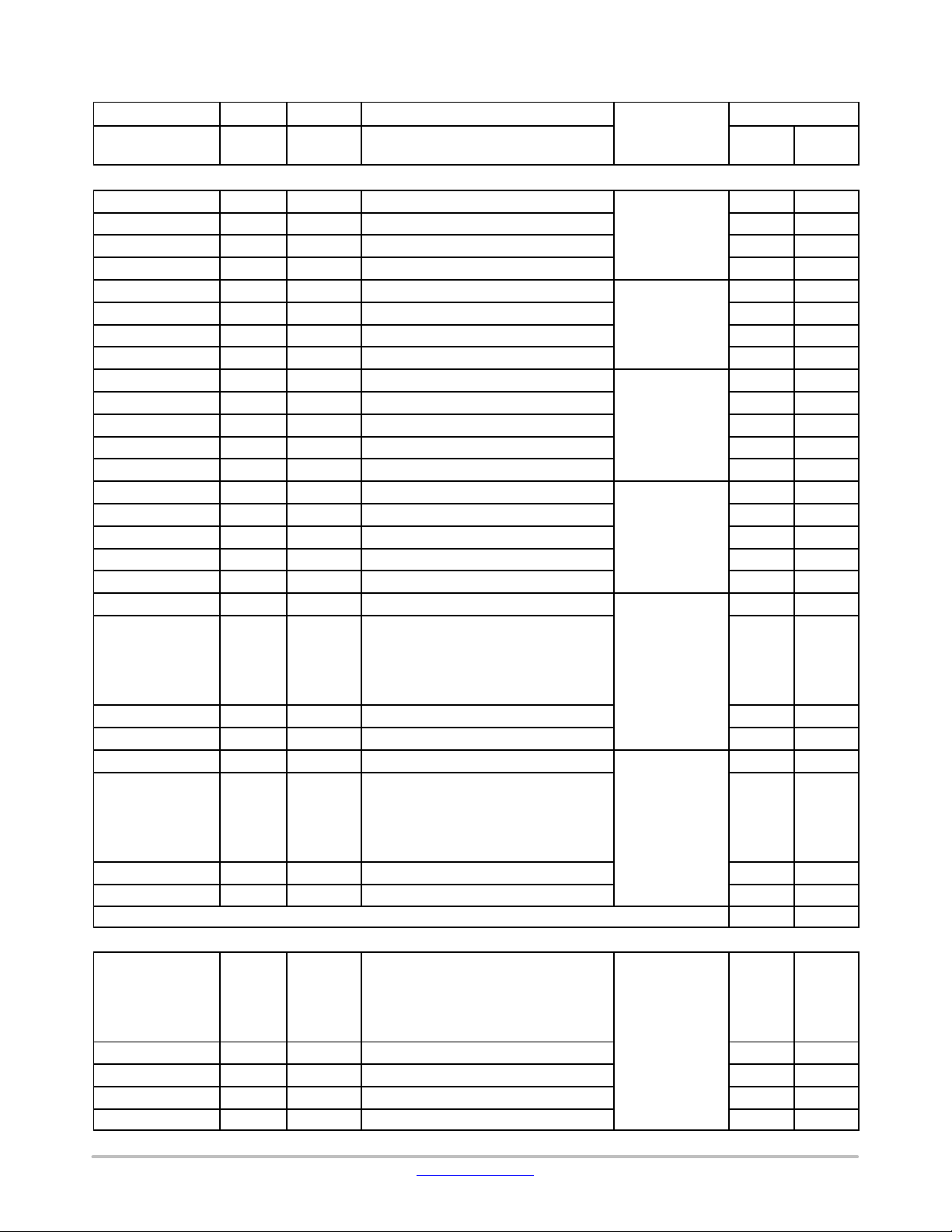
Table 11. TERMINAL FUNCTIONS
Terminal Name
UART
TXD1
−OUART Ch1 transmit Data
SDAT20
−BSD I/F Ch2 Data 0
GPIO04
−BGPIO
EXTINT04
−IExternal Interrupt 0−bit4
RXD1
−IUART Ch1 receive Data
SDAT21
−BSD I/F Ch2 Data 1
GPIO05
−BGPIO
EXTINT05
−IExternal Interrupt 0−bit5
CTS1
Neg
I
UART Ch1 clear to send
SDAT22
−BSD I/F Ch2 Data 2
RXD0
−IUART Ch0 receive Data
GPIO56
−BGPIO
EXTINT56
−IExternal Interrupt 5−bit6
RTS1
Neg
O
UART Ch1 request to send
SDAT23
−BSD I/F Ch2 Data 3
TXD0
−OUART Ch0 transmit Data
GPIO57
−BGPIO
EXTINT57
−IExternal Interrupt 5−bit7
TXD2
−OUART Ch2 transmit Data
TIOCA10
−BMTM1 Ch0A
GPIO0B
−BGPIO
EXTINT0B
−IExternal Interrupt 0−bit11
RXD2
−IUART Ch2 receive Data
TIOCA11
−BMTM1 Ch1A
GPIO0C
−BGPIO
EXTINT0C
−IExternal Interrupt 0−bit12
Sum
6
6
TIMER
TIOCA00
−BMTM0 Ch0A
SDCLK2
−OSD I/F Ch2 Clock Output
PHI0
−OSystem Clock Output 0
GPIO09
−BGPIO
EXTINT09
−IExternal Interrupt 0−bit9
Multiplexed
Function
(continued)
LC823455
FunctionDirectionPolarity
IO POWER
Available(d)
RBXA
− target signal of pulse−length−reader
function
− output of sentinel−inform−function
− output of PWM output
− target signal of pulse−length−reader
function
− output of sentinel−inform−function
− output of PWM output
Vdd2
Vdd2
Vdd2
Vdd2
Vdd2
Vdd2
d d
d d
d d
d d
d d
d d
d d
d d
d d
d d
d d
d d
d d
d d
d d
d d
d d
d d
d d
d d
d d
d d
d d
d d
d d
d d
− target signal of pulse−length−reader
function
− output of sentinel−inform−function
− output of PWM output
www.onsemi.com
24
Vdd2
d d
d d
d d
d d
d d
Page 25
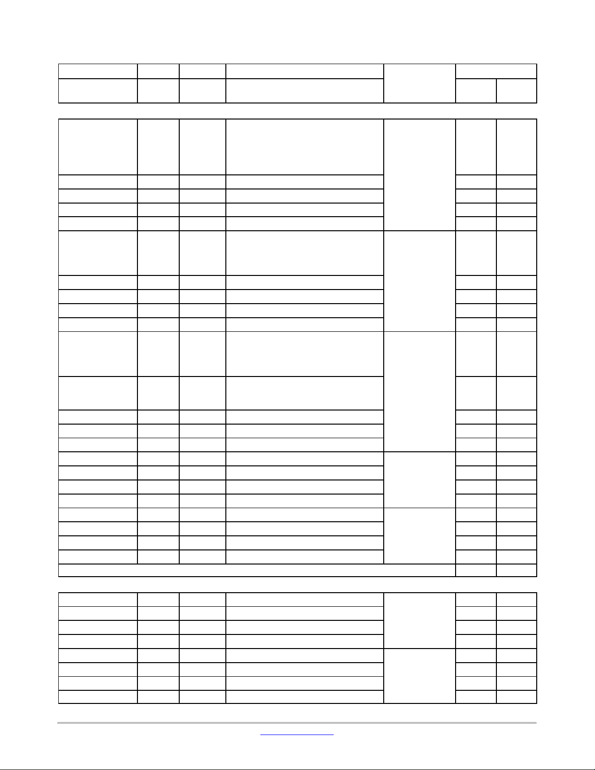
Table 11. TERMINAL FUNCTIONS
Terminal Name
TIOCA01
−BMTM0 Ch1A
SDCMD2
−BSD I/F Ch2 command line
PHI1
−OSystem Clock Output 1
GPIO0A
−BGPIO
EXTINT0A
−IExternal Interrupt 0−bit10
TIOCB00
−BMTM0 Ch0B
DIN1
−IPCM1 Data Input
DMDIN0A
−IDigital Mic Ch0 Data A Input
GPIO02
−BGPIO
EXTINT02
−IExternal Interrupt 0−bit2
TIOCB01
−BMTM0 Ch1B
SFQSCS
Neg
O
Serial Flash I/F QSPI chip select
GPIO03
−BGPIO
EXTINT03
−IExternal Interrupt 0−bit3
SDCMD0
−BSD I/F Ch0 command line
TCLKA0
−IMTM0 external Clock A
BCK1
−BPCM1 bit Clock
GPIO00
−BGPIO
EXTINT00
−IExternal Interrupt 0−bit0
TCLKB0
−IMTM0 external Clock B
LRCK1
−BPCM1 LR Clock
GPIO01
−BGPIO
EXTINT01
−IExternal Interrupt 0−bit1
Sum
6
6
PCM I/F
MCLK0
Pos
B
PCM0 maser Clock
MCLK1
Pos
B
PCM1 master Clock
GPIO18
−BGPIO
EXTINT18
−IExternal Interrupt 1−bit8
BCK0
−BPCM0 bit Clock
DMCKO0B
−
O
Digital Mic Ch0 Clock B Output
GPIO19
−BGPIO
EXTINT19
−IExternal Interrupt 1−bit9
Multiplexed
Function
TIMER
(continued)
− target signal of pulse−length−reader
− output of sentinel−inform−function
− output of PWM output
− target signal of pulse−length−reader
− output of sentinel−inform−function
− target signal of pulse−length−reader
− output of sentinel−inform−function
During Serial Flash Boot, this is used as
chip select of Serial Flash
function
function
function
LC823455
FunctionDirectionPolarity
IO POWER
Vdd2
Vdd2
Vdd2
Vdd2
Vdd2
Available(d)
RBXA
d d
d d
d d
d d
d d
d d
d d
d d
d d
d d
d d
d d
d d
d d
d d
d d
d d
d d
d d
d d
d d
d d
d d
www.onsemi.com
25
Vdd2
Vdd2
d d
d d
d d
d d
d d
d d
d d
d d
Page 26
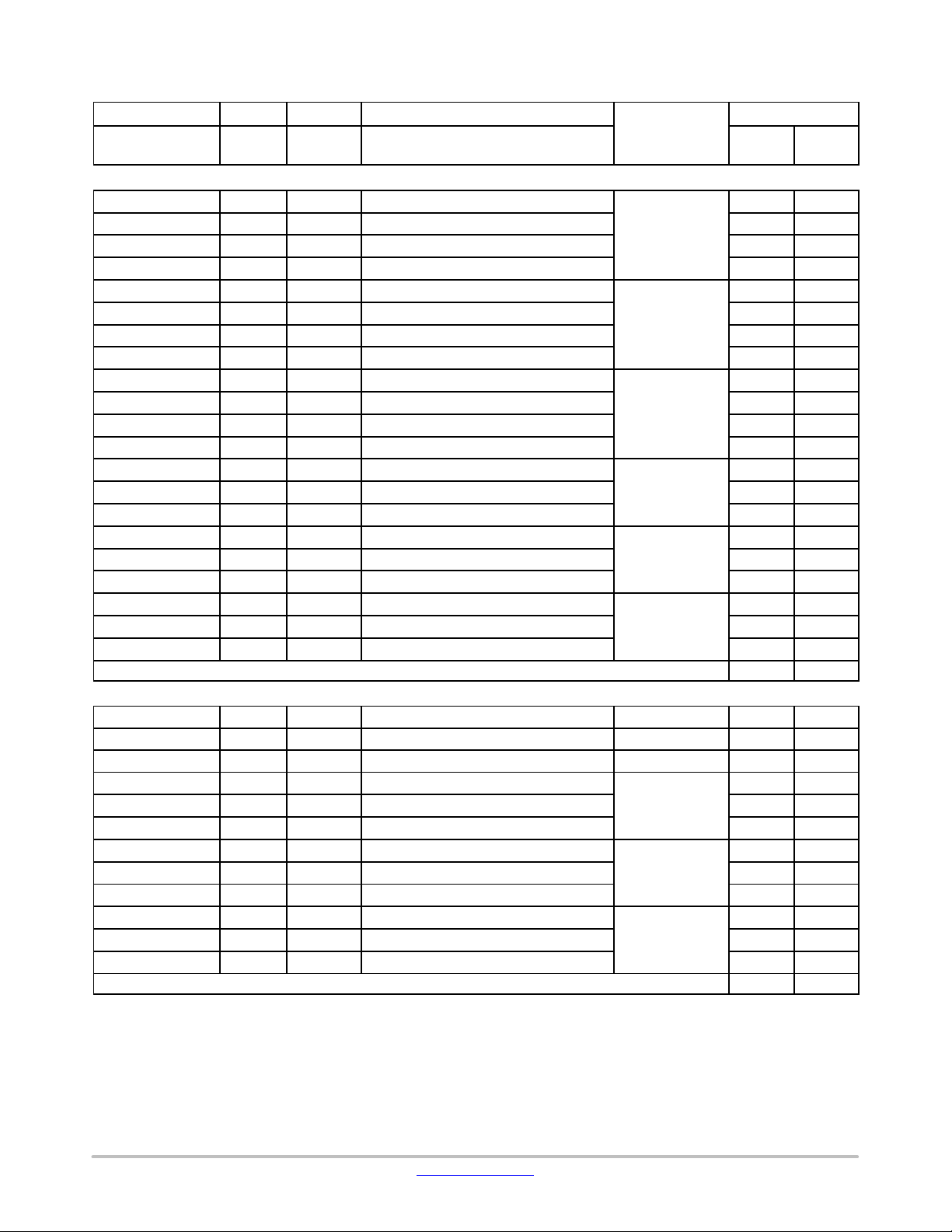
Table 11. TERMINAL FUNCTIONS
Terminal Name
LRCK0
−BPCM0 LR Clock
DMDIN0B
−IDigital Mic Ch0 Data B Input
GPIO1A
−BGPIO
EXTINT1A
−IExternal Interrupt 1−bit10
DIN0
−IPCM0 Data Input
DMDIN0A
−IDigital Mic Ch0 Data A Input
GPIO1B
−BGPIO
EXTINT1B
−IExternal Interrupt 1−bit11
DOUT0
−OPCM0 Data Output
DMCKO0A
−ODigital Mic Ch0 Clock A Output
GPIO1C
−BGPIO
EXTINT1C
−IExternal Interrupt 1−bit12
BCK1
−BPCM1 bit Clock
GPIO13
−BGPIO
EXTINT13
−IExternal Interrupt 1−bit3
LRCK1
−BPCM1 LR Clock
GPIO14
−BGPIO
EXTINT14
−IExternal Interrupt 1−bit4
DOUT1
−OPCM1 Data Output
GPIO15
−BGPIO
EXTINT15
−IExternal Interrupt 1−bit5
Sum
8
8
SD IF
SDCLK0
−OSD I/F Ch0 Clock Output
Vdd2
SDCMD0
−BSD I/F Ch0 command line
Vdd2
SDAT0[3:0]
−BSD I/F Ch0 Data
Vdd2
SDCLK1
−OSD I/F Ch1 Clock Output
GPIO22
−BGPIO
EXTINT22
−IExternal Interrupt 2−bit2
SDCMD1
−BSD I/F Ch1 command line
GPIO23
−BGPIO
EXTINT23
−IExternal Interrupt 2−bit3
SDAT1[3:0]
−BSD I/F Ch1 Data
GPIO2[7:4]
−BGPIO
EXTINT2[7:4]
−IExternal Interrupt 2−bit7 to bit4
Sum
6
12
Multiplexed
Function
PCM I/F
(continued)
LC823455
FunctionDirectionPolarity
IO POWER
Vdd2
Vdd2
Vdd2
Vdd2
Vdd2
Vdd2
Available(d)
RBXA
d d
d d
d d
d d
d d
d d
d d
d d
d d
d d
d d
d d
d d
d d
d d
d d
d d
d d
d d
d d
d d
VddSD1
VddSD1
VddSD1
d
d
d
d d
d d
d d
d d
d d
d d
d d
d d
d d
www.onsemi.com
26
Page 27
Table 11. TERMINAL FUNCTIONS
Terminal Name
PSEUDO SRAM
PSM_SCK
−OP−SRAM I/F Clock Output
Vdd2
PSM_CS
Neg
O
P−SRAM I/F chip select Output
Vdd2
PSM_SDI(DAT0)
−
I(B)
P−SRAM I/F Data input(QPI Data0)
Vdd2
PSM_SDO(DAT1)
−
O(B)
P−SRAM I/F Data output(QPI Data1)
Vdd2
PSM_DAT2
−BP−SRAM I/F QPI Data 2
Vdd2
PSM_DAT3
−BP−SRAM I/F QPI Data 3
Vdd2
Sum
0
0
SDRAM I/F
SDRCLK
Neg
O
SDRAM Clock Output
Vdd2
SDRCKE
Pos
O
SDRAM Clock enable Output
Vdd2
SDRCS
Neg
O
SDRAM chip select Output
Vdd2
SDRWE
Neg
O
SDRAM write enable Output
Vdd2
SDRCAS
Neg
O
SDRAM CAS Output
Vdd2
SDRRAS
Neg
O
SDRAM RAS Output
Vdd2
SDRDQM[1:0]
Pos
O
SDRAM Data mask byte lane select
Vdd2
SDRADDR[10:0]
−OSDRAM address (Note 5)
Vdd2
SDRBA[1:0]
−OSDRAM bank select
Vdd2
SDRDATA[15:0]
−BSDRAM Data
Vdd2
Sum
0
0
EXTERNAL MEMORY I/F
NCS0
Neg
O
chip select0
GPIO06
−BGPIO
EXTINT06
−−IExternal Interrupt 0−bit6
NCS1
Neg
O
chip select1
(Note 6)
(Note 6)
RXD0
−IUART Ch0 receive Data
GPIO10
−BGPIO
EXTINT10
−IExternal Interrupt 1−bit0
NRD
Neg
O
read enable
(Note 6)
(Note 6)
GPIO17
−BGPIO
EXTINT17
−IExternal Interrupt 1−bit7
NWRENWRL
Neg
O
write enable, write enable low
(Note 6)
(Note 6)
DIN0
−IPCM0 Data Input
GPIO30
−BGPIO
EXTINT30
−IExternal Interrupt 3−bit0
NHBNWRH
Neg
O
high byte select, write enable high
(Note 6)
(Note 6)
TXD0
−OUART Ch0 transmit Data
DOUT0
−OPCM0 Data Output
GPIO31
−BGPIO
EXTINT31
−IExternal Interrupt 3−bit1
NLBEXA0
−Olow byte select, address0
(Note 6)
(Note 6)
GPIO16
−BGPIO
EXTINT16
−IExternal Interrupt 1−bit6
Multiplexed
Function
(continued)
LC823455
FunctionDirectionPolarity
IO POWER
Available(d)
RBXA
Vdd2
Vdd2
Vdd2
Vdd2
Vdd2
Vdd2
d d
d d
d d
d d
d d
d d
d d
d d
d d
d d
d d
d d
d d
d d
www.onsemi.com
27
Page 28
Table 11. TERMINAL FUNCTIONS
Terminal Name
EXA[20:15]
−Oaddress
GPIO4[5:0]
−BGPIO
EXTINT4[5:0]
−IExternal Interrupt 4−bit5 to bit0
EXA[14:9]
−Oaddress
GPIO3[F:A]
−BGPIO
EXTINT3[F:A]
−IExternal Interrupt 3−bit15 to bit10
EXA[8:5]
−Oaddress
GPIO3[9:6]
−BGPIO
EXTINT3[9:6]
−IExternal Interrupt 3−bit9 to bit6
EXA4
−Oaddress
DOUT1
−OPCM1 Data Output
GPIO35
−BGPIO
EXTINT35
−IExternal Interrupt 3−bit5
EXA3
−Oaddress
(Note 6)
DIN1
−IPCM1 Data Input
GPIO34
−BGPIO
EXTINT34
−IExternal Interrupt 3−bit4
EXA[2:1]
−Oaddress
GPIO3[3:2]
−BGPIO
EXTINT3[3:2]
−IExternal Interrupt 3−bit3 to bit2
EXD[7:0]
−BData
GPIO4[D:6]
−BGPIO
EXTINT4[D:6]
−IExternal Interrupt 4−bit13 to bit6
EXD[15:10]
−BData
GPIO5[5:0]
−BGPIO
EXTINT5[5:0]
−IExternal Interrupt 5−bit5 to bit0
EXD[9:8]
−BData
GPIO4[F:E]
−BGPIO
EXTINT4[F:E]
−IExternal Interrupt 4−bit15 to bit14
Sum
5
6
XTAL, PLL
XIN1
−IXTAL input (XT1)
VddXT1
XOUT1
−OXTAL output (XT1)
VddXT1
VddXT1
−PXTAL power supply (XT1)
−
VssXT1
−PXTAL ground (XT1)
−
XTALINFO[1: 0]
−BXTALINFO[1: 0] =
Vdd2
Multiplexed
Function
EXTERNAL MEMORY I/F
(continued)
LC823455
FunctionDirectionPolarity
IO POWER
Vdd2
Vdd2
Vdd2
Vdd2
Vdd2
Vdd2
Available(d)
RBXA
d
d
d
Vdd2
Vdd2
Vdd2
d d
d d
d d
d d
“00” : 24 MHz
“01” : 12 MHz
“10” : 19.2 MHz
“11” : reserved
Used for determining clock frequency set-
ting during internal ROM boot.
Bonding “00” internally.
www.onsemi.com
28
Page 29
Table 11. TERMINAL FUNCTIONS
Terminal Name
VCNT1
−OPLL1 VCO control
AVddPLL1
AVddPLL1
−PPLL1 analog power supply
−
AVssPLL1
−PPLL1 analog power ground
−
VCNT2
−OPLL2 VCO control
AVddPLL2
AVddPLL2
−PPLL2 analog power supply
−
AVssPLL2
−PPLL2 analog power ground
−
Sum
8
8
USB−PHY
USBDP
−BUSB D+
AVddUSBPHY2
USBDM
−BUSB D−
AVddUSBPHY2
USBEXT02
−BUSB reference resistor
AVddUSBPHY18
USBVBUS
−IUSB 5V VBUS detection
−
USBID
−BUSB identifier
AVddUSBPHY18
DVddUSBPHY1
−PUSB−PHY 1.0V digital power supply
−
AVddUSBPHY2
−PUSB−PHY 3.3V analog power supply
−
AVddUSBPHY18
−PUSB−PHY 1.8V analog power supply
−
AVssUSBPHY
−PUSB−PHY ground
−
Sum
10
10
12 BIT ADC
SIN[7: 3]
−IADC input ch7−3
AVddADC
SIN[2: 0]
−IADC input ch2−0
AVddADC
AVddADC
−PADC analog power supply
−
AVssADC
−PADC analog power ground
−
Sum
5
10
CLASS−D AMP
LOUT
−OLch Class D AMP Output
GPLOUT
−OGeneral purpose Output (GPO)
ROUT
−ORch Class D AMP Output
GPROUT
−OGeneral purpose Output (GPO)
AVddDAMPL
−PLch Class D AMP analog power supply
−
AVddDAMPR
−PRch Class D AMP analog
−
AVssDAMPL
−PLch Class D AMP analog power ground
−
AVssDAMPR
−PRch Class D AMP analog
−
Sum
6
6
OTHER, POWER
BMODE[1: 0]
−BBoot mode select
Vdd2
TEST
Pos
I
test mode
VddRTC
NRES
Neg
I
SoC reset input
Vdd2
Multiplexed
Function
XTAL, PLL
(continued)
Only internal loop filter.
Only internal loop filter.
LC823455
FunctionDirectionPolarity
IO POWER
Available(d)
RBXA
d d
d d
d d
d d
d d
d d
d d
d d
d d
d d
d d
d d
d
2
d
2
power supply
power ground
Connect to ground.
AVddDAMPL
AVddDAMPR
d
d d
d d
d d
d d
d d
d d
d d
d d
d d
d d
d d
d d
d d
d d
www.onsemi.com
29
Page 30
Table 11. TERMINAL FUNCTIONS
Terminal Name
IO18V
−I1.8 V IO range select for I/O of Vdd2
Vdd1
Vdd1
−PDigital core power supply
−
Vdd2
−PDigital IO power supply
−
VddSD1
−PDigital IO power supply(SDI/F ch1)
−
Vss1
−PDigital core power ground
−
Vss2
−PDigital IO power ground
−
Sum
31
33
All Sum
120
136
Multiplexed
Function
OTHER, POWER
(continued)
“0” : 3.3 V IO operation
“1” : 1.8 V IO operation
When setting “1”, don’t supply any voltage
over the 1.8 V voltage range to Vdd2.
LC823455
FunctionDirectionPolarity
IO POWER
Available(d)
RBXA
d d
d
6
d
6
d
1
d
6
d
7
d
6
d
7
d
1
d
6
d
8
3. Set according to the General RTC mode or KeyInt RTC mode.
4. S−Flash I/F / SD I/F Ch0 includes SFQSCS / SDCMD0 in Timer.
5. SDRAM address bit is 13 bit including SDRADDR [12:11].
6. This function is not available.
www.onsemi.com
30
Page 31

LC823455
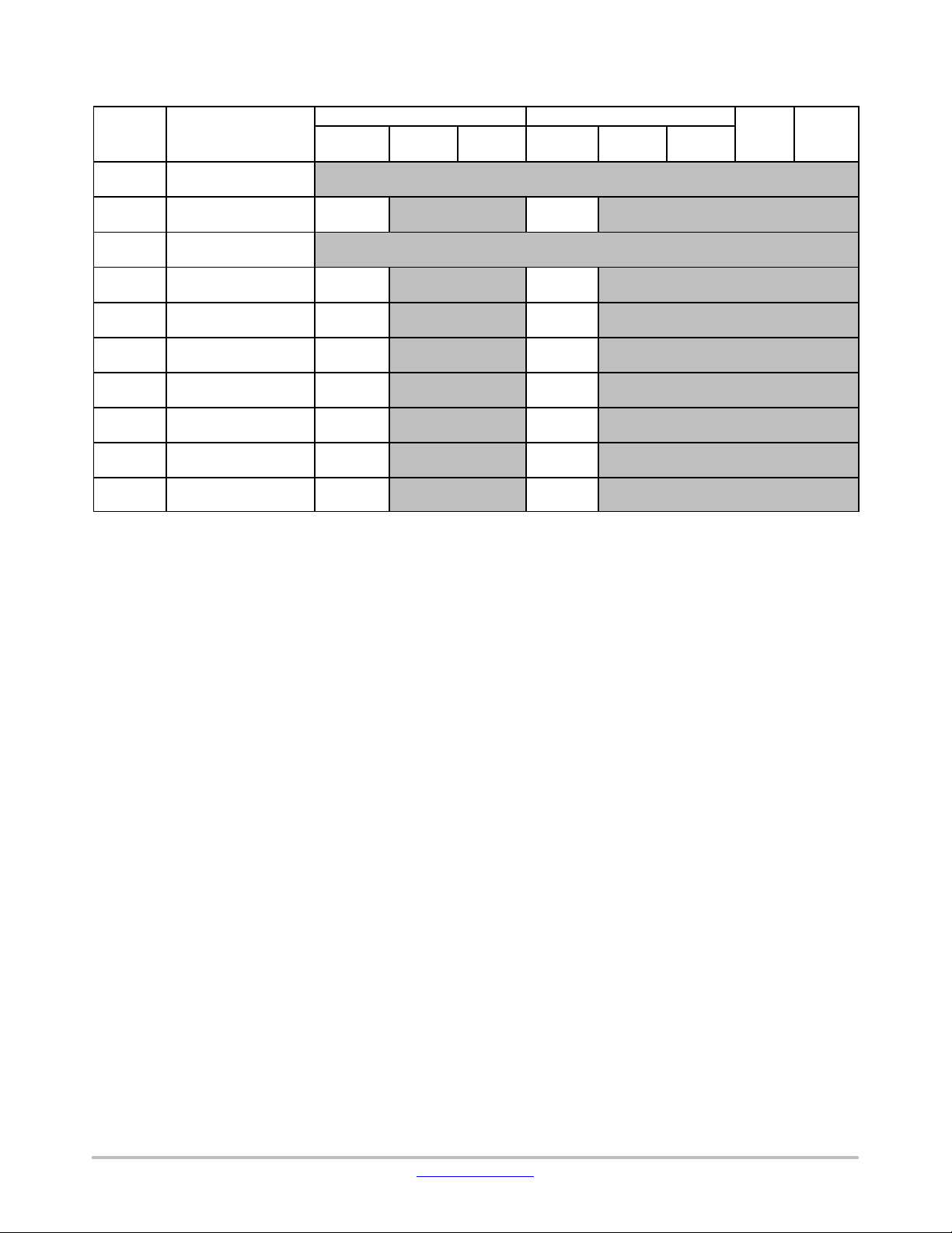
Table 12. PIN MULTIPLEX FUNCTIONS
Number
Module name
Signal name
Function
Assigned GPIO
0
SCL0
I2C ch0 Clock
1
SDA0
I2C ch0 Data
2
SCL1
I2C ch1 Clock
3
SDA1
I2C ch1 Data
4
SCK0
Serial I/F Ch0 Clock
5
SDI0
Serial I/F Ch0 Data Input
6
SDO0
Serial I/F Ch0 Data Output
7
SCK1
Serial I/F Ch1 Clock
8
SDI1
Serial I/F Ch1 Data Input
9
SDO1
Serial I/F Ch1 Data Output
10
TCLKA0
MTM0 external Clock A
11
TCLKB0
MTM0 external Clock B
12
TIOCA00
MTM0 Ch0A
13
TIOCA01
MTM0 Ch1A
14
TIOCB00
MTM0 Ch0B
15
TIOCB01
MTM0 Ch1B
16
TCLKA1
MTM1 external Clock A
17
TCLKB1
MTM1 external Clock B
18
TIOCA10
MTM1 Ch0A
19
TIOCA11
MTM1 Ch1A
20
TIOCB10
MTM1 Ch0B
21
TIOCB11
MTM1 Ch1B
22
RXD0
UART Ch0 receive Data
23
TXD0
UART Ch0 transmit Data
24
RXD1
UART Ch1 receive Data
25
TXD1
UART Ch1 transmit Data
26
CTS1
UART Ch1 clear to send
27
RTS1
UART Ch1 request to send
28
RXD2
UART Ch2 receive Data
29
TXD2
UART Ch2 transmit Data
30
CTS2
UART Ch2 clear to send
31
RTS2
UART Ch2 request to send
32
DMCKO0
Digital Mic Ch0 Clock Output
33
DMDIN0
Digital Mic Ch0 Data Input
34
DMCKO1
Digital Mic Ch1 Clock Output
35
DMDIN1
Digital Mic Ch1 Data Input
36
OSC
WICPOWERDOWN
Power control for WIC Sleep
37
Reserved
Reserved
Reserved
Signals Handled by Pin Multiplex Function
The pin multiplex function can be used to assign
low−speed signals to any of GPIOs. The table below shows
the signal functions that can be multiplexed and the GPIOs
that can be assigned.
I2C0
I2C1
SPI0
SPI1
MTM0
MTM1
GPIO00 to 0F
GPIO10 to 1F
GPIO20 to 2F
GPIO30 to 3F
GPIO40 to 4F
GPIO50 to 59
UART0
UART1
UART2
DMIC0
DMIC1
www.onsemi.com
31
Page 32

Boot Mode
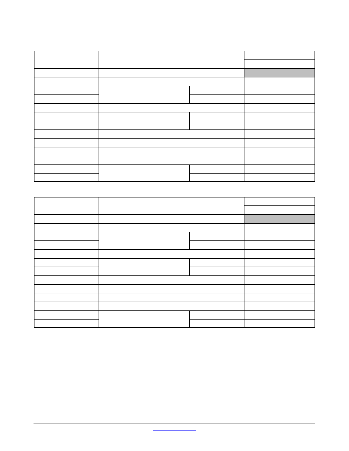
Table 13. BOOT MODE
IPL mode
BMODE1
BMODE0
Explanation
Internal ROM boot (EMMC Physical Boot with USB download)
IPL2 is transferred to boot partition1 area of eMMC via USB from PC.
Internal ROM boot (EMMC Physical Boot with SD Ch1 download)
IPL2 is transferred to boot partition1 area of eMMC from SDCH1.
Internal ROM boot (User Area Boot with USB download)
IPL2 is transferred to user area of eMMC via USB from PC.
Internal ROM boot (User Area Boot with SD Ch1 download)
IPL2 is transferred to user area of eMMC from SDCH1.
Internal ROM boot (External Serial Flash SPI Boot with USB download)
IPL2 is transferred to user area of S−FLASH via USB from PC.
Internal ROM boot (External Serial Flash SPI Boot with SD Ch1 download)
IPL2 is transferred to user area of S−FLASH from SDCH1.
Internal ROM boot
The IPL supports the direct write of the program using the DD command from USB.
The available boot modes are determined by the values on
the BMODE[1:0] terminal.
LC823455
Physical
Boot
USB
Physical
Boot
SD
User Area
Boot
USB
User Area
Boot
SD
SPI Boot
USB
PD
470 k
PD
470 k
PD
1 k
PU
470 k
PU
470 k
PD
470 k
PU
470 k
PU or PD
470 k
PD
1 k
PU
470 k
(SD card I/F Ch0 + USB Device + EXTINT2F)
Using Boot operation mode of eMMC, IPL2(program) is copied to internal SRAM
from boot partition1 area of eMMC connected to SDCH0 and is executed.
XT1 must be connected in this mode to boot the ROM.
The connection of XTRTC is arbitrary.
(SD card I/F Ch0 + SD card I/F Ch1 + EXTINT2F)
Using Boot operation mode of eMMC, IPL2(program) is copied to internal SRAM
from boot partition1 area of eMMC connected to SDCH0 and is executed.
Either XT1 or XTRTC is required to boot the ROM.
(SD card I/F Ch0 + USB Device + EXTINT2F)
IPL2(program) is copied to internal SRAM from user area of eMMC connected to
SDCH0 and is executed.
XT1 must be connected in this mode to boot the ROM.
The connection of XTRTC is arbitrary.
(SD card I/F Ch0 + SD card I/F Ch1 + EXTINT2F)
IPL2(program) is copied to internal SRAM from user area of eMMC connected to
SDCH0 and is executed.
Either XT1 or XTRTC is required to boot the ROM.
(S−FLASH I/F + USB Device + EXTINT2F )
IPL2(program) is copied to internal SRAM from user area of S−FLASH and is
executed.
XT1 must be connected in this mode to boot the ROM.
The connection of XTRTC is arbitrary.
SPI Boot
SD
QSPI Boot
USB
PD
470 k
PU
1 k
PU
1 k
PU
470 k
(S−FLASH I/F + SDcard I/F Ch1 + EXTINT2F)
IPL2(program) is copied to internal SRAM from user area of S−FLASH and is
executed.
Either XT1 or XTRTC is required to boot the ROM.
(External Serial Flash QSPI Boot with USB download)
(S−Flash I/F(QSPI) + USB Device + EXTINT2F)
In this mode, the CPU fetches Serial Flash connected to S/Flash IF directly.
XT1 must be connected in this mode to boot the ROM.
The connection of XTRTC is arbitrary.
www.onsemi.com
32
Page 33

Table 13. BOOT MODE (continued)
Internal ROM boot
IPL2 is transferred to S−FLASH from SDCH1.
Internal ROM boot (User Area IPL2 deletion)
It comes to be able to write IPL2 again at User Area Boot.
Internal ROM boot (Partition Area IPL2 deletion)
It comes to be able to write IPL2 again at eMMC Physical Boot.
Internal ROM boot (All external Serial Flash SPI area deletion)
All of Serial Flash is deleted.
Internal ROM boot (All area deletion )
All of eMMC is deleted. The partition area is also erased, which takes time. When
Internal ROM boot (All external Serial Flash QSPI area deletion)
All of Serial Flash is deleted.
N/A
N/A
Hi−z
PU
PU
External memory I/F terminal are Hiz
IPL mode ExplanationBMODE0BMODE1
QSPI Boot
SD
User Area
Delete
Partition
Delete
SPI All
Erase
SDCH0 All
Erase
PU
1 k
PD
1 k
PD
470 k
PU
470 k
PD
1 k
PD
470 k
PU
1 k
PD
1 k
PU
1 k
PD
1 k
LC823455
(External Serial Flash QSPI Boot with SD Ch1 download)
(S−Flash I/F(QSPI) + SD card I/F Ch1 + EXTINT2F)
In this mode, the CPU fetches from Serial Flash connected to S/Flash IF directly.
Either XT1 or XTRTC is required to boot the ROM.
( SD card I/F Ch0 + EXTINT2F)
Either XT1 or XTRTC is necessary to boot the ROM.
(SD card I/F Ch0 + EXTINT2F)
Either XT1 or XTRTC is necessary to boot the ROM.
( S−Flash I/F, + EXTINT2F )
Please select it when you use Serial Flash with SPI.
Either XT1 or XTRTC is required to boot the ROM.
(SD card I/F Ch0 + EXTINT2F)
eMMC corresponds to Trim, Trim is done.
Either XT1 or XTRTC is required to boot the ROM.
QSPI All
Erase
External
ROM Boot
PU
1 k
PU
470 k
1 k
PD
1 k
PD
470 k
1 k
(S−Flash I/F(QSPI) + EXTINT2F)
Please use it when you use Serial Flash in the fetch mode of QSPI.
Either XT1 or XTRTC is required to boot the ROM.
EXA[20:1], EXD[15:0], NCS[1:0], NRD, NWRENWRL, NHBNWRH, NLBEXA0
SD card I/F Ch0 terminal are Hiz
SDCLK0, SDCMD0, SDAT0[3:0]
S−Flash(QSPI) terminal are Hiz
SFQSCS, SFCK, SFDI(QIO0), SFDO(QIO1), SFWP(QIO2), SFHOLD(QIO3)
Either XT1 or XTRTC is required to boot the ROM.
Boot Port
The ports used while booting are described below.
• There is no dedicated SDCH0 pin in the WLP package.
Therefore, when booting from eMMC, the terminals
SFCK, SFQSCS, SFDO, SFDI, SFWP, and SFHOLD
must be switched to SDCLK0, SDCMD0, SDAT00,
SDAT01, SDAT02, and SDAT03. The target is Physical
Boot USB · Physical Boot SD · User Area Boot USB ·
User Area Boot SD · User Area Delete, Partition
Delete, SDCH 0 All Erase
• SD Card SDCH1 uses only CMD, DATA, and CLK.
The terminals CD and WP are not used. These three
terminals are controlled only when writing IPL2 from
SDCH1
• SPI Boot / SPI All Erase uses only SFCK, SFDO, SFDI
and SFQSCS switched from TIOCB01. SFHOLD and
SFWP (The function is different according to the
device) are not used
• QSPI Boot / QSPI All Erase uses SFCK, SFDO, SFDI,
SFHOLD, SFWP and SFQSCS switched from
TIOCB01
www.onsemi.com
33
Page 34

Table 14. GPIOs USED DURING IPL
(RB is under planning.)
SDCH0
Shared (for XA)
Dedicated (for RB)
Physical Boot USB
P2F(error notification)
P2F(error notification)
Physical Boot SD
P2F(error notification),
P2F(error notification)
User Area Boot USB
P2F(error notification),
P2F(error notification)
User Area Boot SD
P2F(error notification)
P2F(error notification)
SPI Boot USB
P2F(error notification)
P2F(error notification)
SPI Boot SD
P2F(error notification),
P2F(error notification)
QSPI Boot USB
P2F(error notification),
P2F(error notification)
QSPI Boot SD
P2F(error notification)
P2F(error notification)
UserArea Delete
P2F(error notification),
P2F(error notification)
Partition Delete
P2F(error notification),
P2F(error notification)
SPI Erase
P2F(error notification),
P2F(error notification),
SDCH0 All Erase
P2F(error notification),
P2F(error notification)
QSPI All Erase
P2F(error notification),
P2F(error notification),
External ROM Boot
N/A
N/A
HI−z
SDCLK0 is set to the Hi−z input.
IPL mode
LC823455
P0D(SDCLK0), P0E(SDAT00), P0F(SDAT01),
P11(SDAT02), P12(SDAT03), P03(SCMD0)
P22(SDCLK1), P23(SDCMD1), P24(SDDATA10),
P25(SDDATA11), P26(SDDATA12),
P27(SDDATA13), P0D(SDCLK0), P0E(SDAT00),
P0F(SDAT01), P11(SDAT02), P12(SDAT03)
P03(SCMD0)
P0D(SDCLK0), P0E(SDAT00), P0F(SDAT01),
P11(SDAT02), P12(SDAT03), P03(SCMD0)
P0D(SDCLK0), P0E(SDAT00), P0F(SDAT01),
P11(SDAT02), P12(SDAT03), P03(SCMD0),
P22(SDCLK1), P23(SDCMD1), P24(SDDATA10),
P25(SDDATA11),
P26(SDDATA12), P27(SDDATA13)
P0D(SFCK), P03(SFQSCS), P0F(SFDO),
P0E(SFDI)
P0D(SFCK), P03(SFQSCS) P0F(SFDO),
P0E(SFDI), P22(SDCLK1), P23(SDCMD1),
P24(SDDATA10), P25(SDDATA11),
P26(SDDATA12), P27(SDDATA13)
P0D(SFCK), P03(SFQSCS), P0F(SFDO),
P0E(SFDI), P11(SFWP), P12(SFHOLD)
,
P22(SDCLK1), P23(SDCMD1),
P24(SDDATA10), P25(SDDATA11),
P26(SDDATA12), P27(SDDATA13)
,
P22(SDCLK1), P23(SDCMD1),
P24(SDDATA10), P25(SDDATA11),
P26(SDDATA12), P27(SDDATA13)
,
P0D(SFCK), P03(SFQSCS), P0F(SFDO), P0E(SFDI)
,
P0D(SFCK), P03(SFQSCS) P0F(SFDO), P0E(SFDI),
P22(SDCLK1), P23(SDCMD1), P24(SDDATA10),
P25(SDDATA11),
P26(SDDATA12), P27(SDDATA13)
,
P0D(SFCK), P03(SFQSCS), P0F(SFDO), P0E(SFDI),
P11(SFWP), P12(SFHOLD)
7. In this table, “Pxx” means “GPIOxx”. For example “P2F” means “GPIO2F”.
P0D(SFCK), P03(SFQSCS), P0F(SFDO),
P0E(SFDI), P011(SFWP), P12(SFHOLD),
P22(SDCLK1), P23(SDCMD1), P24(SDDATA10),
P25(SDDATA11), P26(SDDATA12),
P27(SDDATA13)
P0D(SDCLK0), P0E(SDAT00), P0F(SDAT01),
P11(SDAT02), P12(SDAT03), P03(SCMD0)
P0D(SDCLK0), P0E(SDAT00), P0F(SDAT01),
P11(SDAT02), P12(SDAT03), P03(SCMD0)
P0D(SFCK), P03(SFQSCS), P0F(SPIOUT),
P0E(SFDI)
P0D(SDCLK0), P0E(SDAT00), P0F(SDAT01),
P11(SDAT02), P12(SDAT03), P03(SCMD0)
P0D(SFCK), P03(SFQSCS), P0F(SFDO),
P0E(SFDI), P11(SFWP), P12(SFHOLD)
www.onsemi.com
34
P0D(SFCK), P03(SFQSCS), P0F(SFDO), P0E(SFDI),
P011(SFWP), P12(SFHOLD), P22(SDCLK1), P23(SDCMD1),
P24(SDDATA10), P25(SDDATA11),
P26(SDDATA12), P27(SDDATA13)
P0D(SFCK), P03(SFQSCS), P0F(SPIOUT), P0E(SFDI)
P0D(SFCK), P03(SFQSCS), P0F(SFDO), P0E(SFDI),
P11(SFWP), P12(SFHOLD)
Page 35

LC823455
SDIF PullUp
If using the SDIF port during boot mode, internal PullUp
resistors are used (SDCMD0, SDAT0[3:0] / SDCMD1,
SDAT1[3:0]). Therefore, external PullUp resistors are not
required on the board.
SFQSCS PullUp
If using SFQSCS during boot mode, the initial condition
for terminal P03 relative to SFQSCS is Pull−Up. After
terminal P03 is switched to SFQSCS, the Pull−Up is
released.
GPIO2F
During boot mode, GPIO2F provides notification of the
beginning of USB connection, notification of the
termination of USB connection, as well as error notification
with High/Low of the terminal.
When errors occur during boot sequences, for example
writing of IPL2, GPIO2F reports the sort of error. Moreover,
GPIO2F can indicate the status of USB connection and the
completion of USB file transfer. Additionally, Delete Mode,
completion of Erase, and status of Erase can also be reported
through a sequence of Low/High.
For more d e t a i l a b o u t t h e behavior of this port used during
boot, refer to the “IPL detail” chapter in the “LC823455
Sample Software Reference”
.
www.onsemi.com
35
Page 36

LC823455
Table 15. PIN ASSIGNMENT
I/O
I
Input
O
Output
B
Bidirectional
P
Power
G
Ground
T able 16.
RB
XA
No.
Ball
No.
Ball
−−−−Vdd2
P
−−−−Vss2
G
−−−−EXD0/
B/
Schmitt
3−State
2/4/8 mAPDVdd2
3ISD/3T2
−−−−EXA1/
O/
Schmitt
3−State
2/4/8 mAPDVdd2
3ISD/3T2
−−−−EXA11/
O/
Schmitt
3−State
2/4/8 mAPDVdd2
3ISD/3T2
−−−−EXA12/
O/
Schmitt
3−State
2/4/8 mAPDVdd2
3ISD/3T2
−−−−EXA13/
O/
Schmitt
3−State
2/4/8 mAPDVdd2
3ISD/3T2
−−−−EXA14/
O/
Schmitt
3−State
2/4/8 mAPDVdd2
3ISD/3T2
1
R151L10
Vdd1
P
2
R162H8
NRD/
O/
Schmitt
3−State
2/4/8 mAPDVdd2
3ISD/3T2
3
P153K9
SWDIO/
B/
Schmitt
3−State
2 mAPUVdd2
3ISU/3T2
4
P164G7
NLBEXA0/
O/
Schmitt
3−State
2/4/8 mAPDVdd2
3ISD/3T2
−−−−EXD2/
B/
Schmitt
3−State
2/4/8 mAPDVdd2
3ISD/3T2
−−−−EXA2/
O/
Schmitt
3−State
2/4/8 mAPDVdd2
3ISD/3T2
5
N155L9
Vss2
G
−−−−EXA6/
O/
Schmitt
3−State
2/4/8 mAPDVdd2
3ISD/3T2
−−−−EXA7/
O/
Schmitt
3−State
2/4/8 mAPDVdd2
3ISD/3T2
−−−−SDRADDR12/
O/
Schmitt
3−State
2/4/8 mA
PU/PD
Vdd2
3ISUD/3T2
PIN ASSIGNMENT
XA: Package Code = “XA”, RB: Package Code = “RB”, (RB is under planning).
BGA136
WLP120
PIN NAME I/O
GPIO46/
EXTINT46
GPIO32/
EXTINT32
GPIO3C/
EXTINT3C
GPIO3D/
EXTINT3D
GPIO3E/
EXTINT3E
GPIO3F/
EXTINT3F
GPIO17/
EXTINT17
DMDIN0B/
GPIO59/
EXTINT59
Input
Type
B/
I
B/
I
B/
I
B/
I
B/
I
B/
I
B/
I
I/
B/
I
Output
Type
Drive PU/PD
IO
Pwr Grp
IO
Circuit Type
(4)(8)
(4)(8)
(4)(8)
(4)(8)
(4)(8)
(4)(8)
(4)(8)
GPIO16/
EXTINT16
GPIO48/
EXTINT48
GPIO33/
EXTINT33
GPIO37/
EXTINT37
GPIO38/
EXTINT38
GPIO2A/
EXTINT2A
B/
I
B/
I
B/
I
B/
I
B/
I
B/
I
(4)(8)
(4)(8)
(4)(8)
(4)(8)
(4)(8)
(4)(8)
www.onsemi.com
36
Page 37

T able 16. (continued)
IO
IO
Output
Input
6
N166J8
TDI/
I/
Schmitt
3−State
2 mA
PU/PD
VddSD1
3ISUD/3T2
7
M157K8
TDO/
O/
Schmitt
3−State
2 mA
PU/PD
VddSD1
3ISUD/3T2
8
M168L8
VddSD1
P
9
L159H7
SDCMD1/
B/
CMOS
3−State
2/4/8/1
PU/PD
VddSD1
3ICUD/3T2
10
L1610J7
SDAT10/
B/
CMOS
3−State
2/4/8/10mA
PU/PD
VddSD1
3ICUD/3T2
11
K1211K7
SDAT11/
B/
CMOS
3−State
2/4/8/10mA
PU/PD
VddSD1
3ICUD/3T2
12
J1512L7
Vss2
G
13
K1613F5
SDAT12/
B/
CMOS
3−State
2/4/8/10mA
PU/PD
VddSD1
3ICUD/3T2
14
J1214G6
SDAT13/
B/
CMOS
3−State
2/4/8/10mA
PU/PD
VddSD1
3ICUD/3T2
15
K1515H6
SDCLK1/
O/
CMOS
3−State
2/4/8/10mA
PU/PD
VddSD1
3ICUD/3T2
16
J1616L6
Vss1
G
17
H12−−
RTCMODE
I
CMOS−−−VddRTC
1IC
18
H1517K6
VddRTC
P
19
H1618J5
XIN32K
IX−−−
VddRTC
X
20
G1519K5
VssRTC
G
21
G1620L5
XOUT32K
O−X−−
VddRTC
X
−−−−Keyint2
I
CMOS−−PDVddRTC
1ICD
22
F15−−
BACKUPB
I
CMOS−−−VddRTC
1IC
23
F1621J6
VDET
I
CMOS−−−VddRTC
1IC
24
E1622H5
RTCINT (Note 8)
O−OD
0.3 mA−OD
−
VddRTC
OD3
25
G1223G5
Keyint0
I
CMOS−−PDVddRTC
1ICD
26
E1524H4
TEST
I
CMOS−−−VddRTC
1IC
27
F1225L4
Keyint1
I
CMOS−−PDVddRTC
1ICD
28
D1526K4
AVddPLL1
P
−−−−VCNT1O−1A−−AVddPLL1
1A
29
D1627J4
AVssPLL1
G
30
C1528K3
AVddPLL2
P
−−−−VCNT2O−1A−−AVddPLL2
1A
31
C1629L3
AVssPLL2
G
−−−−Vss1
G
−−−−Vdd2
P
−−−−Vss2
G
−−−−EXD4/
B/
Schmitt
3−State
2/4/8 mAPDVdd2
3ISD/3T2
−−−−EXD5/
B/
Schmitt
3−State
2/4/8 mAPDVdd2
3ISD/3T2
32
B1530L2
Vdd1
P
RB
BGA136
No.
XA
WLP120
LC823455
BallNo.Ball
I/OPIN NAME
Type
Type
PU/PDDrive
Pwr Grp
Circuit Type
SDCD1/
SWO/
GPIO20/
EXTINT20
SDWP1/
GPIO21/
EXTINT21
GPIO23/
EXTINT23
GPIO24/
EXTINT24
GPIO25/
EXTINT25
GPIO26/
EXTINT26
GPIO27/
EXTINT27
GPIO22/
EXTINT22
I/
O/
B/
I
I/
B/
I
B/
I
B/
I
B/
I
B/
I
B/
I
B/
I
mA
0
(4)(8)(10)
(4)(8)(10)
(4)(8)(10)
(4)(8)(10)
(4)(8)(10)
(4)(8)(10)
GPIO4A/
EXTINT4A
GPIO4B/
EXTINT4B
B/
B/
I
I
www.onsemi.com
37
(4)(8)
(4)(8)
Page 38

T able 16. (continued)
IO
IO
Output
Input
−−−−EXD6/
B/
Schmitt
3−State
2/4/8 mAPDVdd2
3ISD/3T2
−−−−EXA19/
O/
Schmitt
3−State
2/4/8 mAPDVdd2
3ISD/3T2
−−−−EXA20/
O/
Schmitt
3−State
2/4/8 mAPDVdd2
3ISD/3T2
−−−−EXD7/
B/
Schmitt
3−State
2/4/8 mAPDVdd2
3ISD/3T2
−−−−EXD8/
B/
Schmitt
3−State
2/4/8 mAPDVdd2
3ISD/3T2
33
B1431L1
Vss1
G
−−−−EXD11/
B/
Schmitt
3−State
2/4/8 mAPDVdd2
3ISD/3T2
−−−−EXD12/
B/
Schmitt
3−State
2/4/8 mAPDVdd2
3ISD/3T2
−−−−EXD13/
B/
Schmitt
3−State
2/4/8 mAPDVdd2
3ISD/3T2
−−−−EXD14/
B/
Schmitt
3−State
2/4/8 mAPDVdd2
3ISD/3T2
−−−−Vss2
G
34
A1632K2
DOUT1/
O/
Schmitt
3−State
2/4/8 mA
PU/PD
Vdd2
3ISUD/3T2
−−−−EXD9/
B/
Schmitt
3−State
2/4/8 mAPDVdd2
3ISD/3T2
−−−−EXD10/
B/
Schmitt
3−State
2/4/8 mAPDVdd2
3ISD/3T2
35
B1633K1
Vdd2
P
−−−−EXD15/
B/
Schmitt
3−State
2/4/8 mAPDVdd2
3ISD/3T2
36
A1534J3
BCK1/
B/
Schmitt
3−State
2/4/8 mA
PU/PD
Vdd2
3ISUD/3T2
37
A1435G4
MCLK0/
B/
Schmitt
3−State
2/4/8 mA
PU/PD
Vdd2
3ISUD/3T2
38
A1336J2
LRCK1/
B/
Schmitt
3−State
2/4/8 mA
PU/PD
Vdd2
3ISUD/3T2
39
B1337J1
Vss2
G
−−−−Vdd2
P
40
B1238H3
BCK0/
B/
Schmitt
3−State
2/4/8 mA
PU/PD
Vdd2
3ISUD/3T2
41
A1239G3
LRCK0/
B/
Schmitt
3−State
2/4/8 mA
PU/PD
Vdd2
3ISUD/3T2
42
B1140H2
DIN0/
I/
Schmitt
3−State
2/4/8 mA
PU/PD
Vdd2
3ISUD/3T2
−−−−Vss2
G
RB
BGA136
No.
XA
WLP120
LC823455
BallNo.Ball
I/OPIN NAME
Type
Type
PU/PDDrive
Pwr Grp
Circuit Type
GPIO4C/
EXTINT4C
GPIO44/
EXTINT44
GPIO45/
EXTINT45
GPIO4D/
EXTINT4D
GPIO4E/
EXTINT4E
GPIO51/
EXTINT51
GPIO52/
EXTINT52
GPIO53/
EXTINT53
GPIO54/
EXTINT54
GPIO15/
EXTINT15
B/
I
B/
I
B/
I
B/
I
B/
I
B/
I
B/
I
B/
I
B/
I
B/
I
(4)(8)
(4)(8)
(4)(8)
(4)(8)
(4)(8)
(4)(8)
(4)(8)
(4)(8)
(4)(8)
(4)(8)
GPIO4F/
EXTINT4F
GPIO50/
EXTINT50
GPIO55/
EXTINT55
GPIO13/
EXTINT13
MCLK1/
GPIO18/
EXTINT18
GPIO14/
EXTINT14
DMCKO0B/
GPIO19/
EXTINT19
DMDIN0B/
GPIO1A/
EXTINT1A
DMDIN0A/
GPIO1B/
EXTINT1B
B/
I
B/
I
B/
I
B/
I
B/
B/
I
B/
I
O/
B/
I
I/
B/
I
I/
B/
I
(4)(8)
(4)(8)
(4)(8)
(4)(8)
(4)(8)
(4)(8)
(4)(8)
(4)(8)
(4)(8)
www.onsemi.com
38
Page 39

T able 16. (continued)
IO
IO
Output
Input
−−−−XTALINFO1
B
Schmitt
3−State
2/4/8 mAPUVdd2
3ISU/3T2
−−−−Vdd2
P
43
A1141H1
DOUT0/
O/
Schmitt
3−State
2/4/8 mA
PU/PD
Vdd2
3ISUD/3T2
44
A1042F4
BMODE0
B
Schmitt
3−State
2 mA
PU/PD
Vdd2
3ISUD/3T2
45
B1043F3
BMODE1
B
Schmitt
3−State
2 mA
PU/PD
Vdd2
3ISUD/3T2
−−−−SDRADDR1
O−3−State
2/4/8 mA−Vdd2
3T2(4)(8)
−−−−EXA4/
O/
Schmitt
3−State
2/4/8 mAPDVdd2
3ISD/3T2
−−−−SDRADDR0
O−3−State
2/4/8 mA−Vdd2
3T2(4)(8)
46B944G1NRES
I
Schmitt−−−Vdd2
3IS
47A945G2AVssDAMPR
G
48A846F1ROUT/
O/O−1A−−AVddDAMPR
1A
49A747F2AVddDAMPR
P
50A648E2AVddDAMPL
P
51A549E1LOUT/
O/O−1A−−AVddDAMPL
1A
52A450D2AVssDAMPL
G
53B851D1Vss1
G
−−−−SDRADDR2
O−3−State
2/4/8 mA−Vdd2
3T2(4)(8)
−−−−SDRADDR3
O−3−State
2/4/8 mA−Vdd2
3T2(4)(8)
54
E1252E3
SCL1/
O/
Schmitt
3−State
2/4/8 mA
PU/PD
Vdd2
3ISUD/3T2
55
E1153E4
SDA1/
B/
Schmitt
3−State
2/4/8 mA
PU/PD
Vdd2
3ISUD/3T2
56
E1054D3
SDRADDR11/
O/
Schmitt
3−State
2/4/8 mA
PU/PD
Vdd2
3ISUD/3T2
−−−−SDRDATA0
B
CMOS
3−State
2/4/8 mAPDVdd2
3ICD/3T2
57B755C1Vdd1
P
−−−−SDRDATA1
B
CMOS
3−State
2/4/8 mAPDVdd2
3ICD/3T2
58E956C2TCLKA0/
I/
Schmitt
3−State
2/4/8 mA
PU/PD
Vdd2
3ISUD/3T2
59E857D4TCLKB0/
I/
Schmitt
3−State
2/4/8 mA
PU/PD
Vdd2
3ISUD/3T2
60E758C3NHBNWRH/
O/
Schmitt
3−State
2/4/8 mAPDVdd2
3ISD/3T2
−−−−Vdd2
P
61B559B1Vss2
G
−−−−PSM_DAT2
B
CMOS
3−State
2/4/8/10 mA
PU/PD
Vdd2
3ICUD/3T2
RB
BGA136
No.
XA
WLP120
LC823455
BallNo.Ball
I/OPIN NAME
Type
Type
PU/PDDrive
Pwr Grp
Circuit Type
(4)(8)
DMCKO0A
GPIO1C/
EXTINT1C
DOUT1/
GPIO35/
EXTINT35
GPROUT
GPLOUT
GPIO2B/
EXTINT2B
O/
B/
I
O/
B/
I
B/
I
(4)(8)
(4)(8)
(4)(8)
GPIO2C/
EXTINT2C
DMCKO0A/
GPIO2D/
EXTINT2D
BCK1/
GPIO00/
EXTINT00
LRCK1/
GPIO01/
EXTINT01
TXD0/
DOUT0/
GPIO31/
EXTINT31
B/
I
O/
B/
I
B/
B/
I
B/
B/
I
O/
O/
B/
I
(4)(8)
(4)(8)
(4)(8)
(4)(8)
(4)(8)
(4)(8)
(4)(8)
(4)(8)(10)
www.onsemi.com
39
Page 40

T able 16. (continued)
IO
IO
Output
Input
−−−−PSM_SDO
O(B)
CMOS
3−State
2/4/8/10 mA
PU/PD
Vdd2
3ICUD/3T2
−−−−PSM_DAT3
B
CMOS
3−State
2/4/8/10 mA
PU/PD
Vdd2
3ICUD/3T2
−−−−SDRADDR4
O−3−State
2/4/8 mA−Vdd2
3T2(4)(8)
−−−−SDRDATA4
B
CMOS
3−State
2/4/8 mAPDVdd2
3ICD/3T2
−−−−SDRDATA14
B
CMOS
3−State
2/4/8 mAPDVdd2
3ICD/3T2
62B660A1Vdd2
P
−−−−Vdd2
P
−−−−SDRDATA2
B
CMOS
3−State
2/4/8 mAPDVdd2
3ICD/3T2
−−−−SDRDATA3
B
CMOS
3−State
2/4/8 mAPDVdd2
3ICD/3T2
−−−−SDRDATA15
B
CMOS
3−State
2/4/8 mAPDVdd2
3ICD/3T2
−−−−PSM_SDI
I(B)
CMOS
3−State
2/4/8/10 mA
PU/PD
Vdd2
3ICUD/3T2
−−−−PSM_CS
O
CMOS
3−State
2/4/8/10mA
PU/PD
Vdd2
3ICUD/3T2
−−−−PSM_SCK
O
CMOS
3−State
2/4/8/10 mA
PU/PD
Vdd2
3ICUD/3T2
−−−−SDRADDR7
O−3−State
2/4/8 mA−Vdd2
3T2(4)(8)
−−−−SDRDATA5
B
CMOS
3−State
2/4/8 mAPDVdd2
3ICD/3T2
−−−−SDRDATA13
B
CMOS
3−State
2/4/8 mAPDVdd2
3ICD/3T2
63B461A2Vss2
G
64A262B2EXTINT2E/GPIO
I/B
Schmitt
3−State
2/4/8 mA
PU/PD
Vdd2
3ISUD/3T2
65A163B3NCS1/
O/
Schmitt
3−State
2/4/8 mAPUVdd2
3ISU/3T2
−−−−SDRDATA12
B
CMOS
3−State
2/4/8 mAPDVdd2
3ICD/3T2
−−−−SDRDATA6
B
CMOS
3−State
2/4/8 mAPDVdd2
3ICD/3T2
−−−−SDRDATA7
B
CMOS
3−State
2/4/8 mAPDVdd2
3ICD/3T2
66B364A3Vss1
G
−−−−SDRDATA8
B
CMOS
3−State
2/4/8 mAPDVdd2
3ICD/3T2
67B265C4EXTINT2F/
I/BSchmitt
3−State
2/4/8 mA
PU/PD
Vdd2
3ISUD/3T2
68B166B4TCK/
I/
Schmitt
3−State
2/4/8 mA
PU/PD
Vdd2
3ISUD/3T2
−−−−SDRDATA9
B
CMOS
3−State
2/4/8 mAPDVdd2
3ICD/3T2
69A367A4Vdd2
P
−−−−SDRDATA11
B
CMOS
3−State
2/4/8 mAPDVdd2
3ICD/3T2
RB
BGA136
No.
XA
WLP120
LC823455
BallNo.Ball
I/OPIN NAME
Type
Type
PU/PDDrive
Pwr Grp
Circuit Type
(DAT1)
(DAT0)
(4)(8)(10)
(4)(8)(10)
(4)(8)
(4)(8)
(4)(8)
(4)(8)
(4)(8)
(4)(8)(10)
(4)(8)(10)
(4)(8)(10)
(4)(8)
2E
RXD0/
GPIO10/
EXTINT10
GPIO2F
SDCD2/
GPIO29/
EXTINT29
(4)(8)
(4)(8)
I/
B/
I
I/
B/
I
(4)(8)
(4)(8)
(4)(8)
(4)(8)
(4)(8)
(4)(8)
(4)(8)
(4)(8)
www.onsemi.com
40
(4)(8)
Page 41

T able 16. (continued)
IO
IO
Output
Input
−−−−SDRDATA10
B
CMOS
3−State
2/4/8 mAPDVdd2
3ICD/3T2
70C268D5TIOCA01/
B/
CMOS
3−State
2/4/8/10 mA
PU/PD
Vdd2
3ICUD/3T2
71C169C5TXD1/
O/
CMOS
3−State
2/4/8/10 mA
PU/PD
Vdd2
3ICUD/3T2
72D270B5RXD1/
I/
CMOS
3−State
2/4/8/10 mA
PU/PD
Vdd2
3ICUD/3T2
−−−−Vss2
G
73D171A5Vdd1
P
74E672E5CTS1/
I/
CMOS
3−State
2/4/8/10 mA
PU/PD
Vdd2
3ICUD/3T2
75E573C6RTS1/
O/
CMOS
3−State
2/4/8/10 mA
PU/PD
Vdd2
3ICUD/3T2
76E274B6TIOCA00/
B/
CMOS
3−State
2/4/8/10 mA
PU/PD
Vdd2
3ICUD/3T2
−−−−SDRADDR5
O−3−State
2/4/8 mA−Vdd2
3T2(4)(8)
−−−−SDRADDR6
O−3−State
2/4/8 mA−Vdd2
3T2(4)(8)
−−−−SDRADDR9
O−3−State
2/4/8 mA−Vdd2
3T2(4)(8)
77H975A6Vdd2
P
78E176D6TMS/
I/
Schmitt
3−State
2/4/8 mA
PU/PD
Vdd2
3ISUD/3T2
79F577E6TXD2/
O/
Schmitt
3−State
2/4/8 mA
PU/PD
Vdd2
3ISUD/3T2
80F278D7RXD2/
I/
Schmitt
3−State
2/4/8 mA
PU/PD
Vdd2
3ISUD/3T2
−−−−SDRBA1
O−3−State
2/4/8 mA−Vdd2
3T2(4)(8)
−−−−SDRBA0
O−3−State
2/4/8 mA−Vdd2
3T2(4)(8)
81F179A7Vss2
G
−−−−SDRADDR10
O−3−State
2/4/8 mA−Vdd2
3T2(4)(8)
82G580B7SFCK/
O/
CMOS
3−State
2/4/8/10 mA
PU/PD
Vdd2
3ICUD/3T2
83G281C7TIOCB01/
B/
CMOS
3−State
2/4/8/10 mA
PU/PD
Vdd2
3ICUD/3T2
84G182E7SFDO(QIO1)/
O(B)/
CMOS
3−State
2/4/8/10 mA
PU/PD
Vdd2
3ICUD/3T2
−−−−SDRRAS
O−3−State
2/4/8 mA−Vdd2
3T2(4)(8)
85H883A8Vdd2
P
RB
BGA136
No.
XA
WLP120
LC823455
BallNo.Ball
I/OPIN NAME
Type
Type
PU/PDDrive
Pwr Grp
Circuit Type
(4)(8)
SDCMD2/
PHI1/
GPIO0A/
EXTINT0A
SDAT20/
GPIO04/
EXTINT04
SDAT21/
GPIO05/
EXTINT05
SDAT22/
RXD0/
GPIO56/
EXTINT56
SDAT23/
TXD0/
GPIO57/
EXTINT57
SDCLK2/
PHI0/
GPIO09/
EXTINT09
B/
O/
B/
I
B/
B/
I
B/
B/
I
B/
I/
B/
I
B/
O/
B/
I
O/
O/
B/
I
(4)(8)(10)
(4)(8)(10)
(4)(8)(10)
(4)(8)(10)
(4)(8)(10)
(4)(8)(10)
SDWP2/
GPIO28/
EXTINT28
TIOCA10/
GPIO0B/
EXTINT0B
TIOCA11/
GPIO0C/
EXTINT0C
GPIO0D/
EXTINT0D/
SDCLK0
SFQSCS/
GPIO03/
EXTINT03/
SDCMD0
GPIO0F/
EXTINT0F/
SDAT01
I/
B/
I
B/
B/
I
B/
B/
I
B/
I/
O
O/
B/
I/
B
B/
I/
B
(4)(8)
(4)(8)
(4)(8)
(4)(8)(10)
(4)(8)(10)
(4)(8)(10)
www.onsemi.com
41
Page 42

T able 16. (continued)
IO
IO
Output
Input
86H584B8SFDI(QIO0)/
I(B)/
CMOS
3−State
2/4/8/10 mA
PU/PD
Vdd2
3ICUD/3T2
87H285C8SFWP(QIO2)/
O(B)/
CMOS
3−State
2/4/8/10 mA
PU/PD
Vdd2
3ICUD/3T2
88H186D8SFHOLD(QIO3)/
O(B)/
CMOS
3−State
2/4/8/10 mA
PU/PD
Vdd2
3ICUD/3T2
89L287A9Vss1
G
−−−−SDRWE
O−3−State
2/4/8 mA−Vdd2
3T2(4)(8)
−−−−SDRCKE
O−3−State
2/4/8 mA−Vdd2
3T2(4)(8)
90J588B9TIOCB00/
B/
Schmitt
3−State
2/4/8 mA
PU/PD
Vdd2
3ISUD/3T2
−−−−SDRCLK
O−3−State
2/4/8/10 mA
−
Vdd2
3T2(4)(8)(10)
−−−−SDRCS
O−3−State
2/4/8 mA−Vdd2
3T2(4)(8)
91M289
A10
IO18V
I1A−−−
Vdd1
1A
−−−−Vss1
G
92J2−−SDAT02
B
CMOS
3−State
2/4/8/10 mA
PU/PD
Vdd2
3ICUD/3T2
93J1−−SDAT03
B
CMOS
3−State
2/4/8/10 mA
PU/PD
Vdd2
3ICUD/3T2
94K5−−SDAT01
B
CMOS
3−State
2/4/8/10 mA
PU/PD
Vdd2
3ICUD/3T2
95K2−−Vdd2
P
96L1−−Vss2
G
97M190
A11
Vdd1
P
−−−−SDRDQM1
O−3−State
2/4/8 mA−Vdd2
3T2(4)(8)
98K1−−SDAT00
B
CMOS
3−State
2/4/8/10 mA
PU/PD
Vdd2
3ICUD/3T2
99L6−−SDCLK0
O−3−State
2/4/8/10 mA
−
Vdd2
3T2(4)(8)(10)
100L5−−SDCMD0
B
CMOS
3−State
2/4/8/10 mA
PU/PD
Vdd2
3ICUD/3T2
−−−−SDRADDR8
O−3−State
2/4/8 mA−Vdd2
3T2(4)(8)
−−−−SDRCAS
O−3−State
2/4/8 mA−Vdd2
3T2(4)(8)
−−−−Vdd2
P
−−−−Vss2
G
101N191
B11
SIN0I3A−−−AvddADC
3A
102P192
B10
SIN1I3A−−−AvddADC
3A
103R193C9SIN2I3A−−−AvddADC
3A
104N294
C11
AVddADC
P
105P2−−SIN3I3A−−−AvddADC
3A
106R2−−SIN4I3A−−−AvddADC
3A
107P3−−SIN5I3A−−−AvddADC
3A
108R3−−SIN6I3A−−−AvddADC
3A
109P4−−SIN7I3A−−−AvddADC
3A
110R495
C10
AVssADC
G
111P596E8AVssUSBPHY
G
RB
BGA136
No.
XA
WLP120
LC823455
BallNo.Ball
I/OPIN NAME
Type
Type
PU/PDDrive
Pwr Grp
Circuit Type
GPIO0E/
EXTINT0E/
SDAT00
GPIO11/
EXTINT11/
SDAT02
GPIO12/
EXTINT12/
SDAT03
DIN1/
DMDIN0A/
GPIO02/
EXTINT02
B/
I/
B
B/
I/
B
B/
I/
B
I/
I/
B/
I
(4)(8)(10)
(4)(8)(10)
(4)(8)(10)
(4)(8)
(4)(8)(10)
(4)(8)(10)
(4)(8)(10)
www.onsemi.com
42
(4)(8)(10)
(4)(8)(10)
Page 43

T able 16. (continued)
IO
IO
Output
Input
112R597
D11
USBEXT02
B3A3A−−
AVddUSBPHY18
3A
113P698D9AVddUSBPHY2
P
114R699
D10
USBDM
B3A3A−−
AVddUSBPHY2
3A
115P7100E9AVssUSBPHY
G
116R7101
E10
USBDP
B3A3A−−
AVddUSBPHY2
3A
117P8102F8DVddUSBPHY1
P
118R8103
F9
USBVBUS
I−−
−
119P9104
F10
AVddUSBPHY18
P
120R9105
F11
USBID
B3A3A−−
AVddUSBPHY18
3A
121
R10
106G8VddXT1
P
122
R11
107G9XIN1IX−−−VddXT1
X
123
P10
108
G10
VssXT1
G
124
P11
109
G11
XOUT1
O−X−−
VddXT1
X
−−−−Vss1
G
−−−−Vdd1
P
−−−−Vdd2
P
−−−−XTALINFO0
B
Schmitt
3−State
2/4/8 mAPUVdd2
3ISU/3T2
−−−−Vss2
G
125L7110F7SDO0/
O/
Schmitt
3−State
2/4/8 mA
PU/PD
Vdd2
3ISUD/3T2
126L8111F6SCK0/
B/
Schmitt
3−State
2/4/8 mA
PU/PD
Vdd2
3ISUD/3T2
−−−−SDRDQM0
O−3−State
2/4/8 mA−Vdd2
3T2(4)(8)
−−−−EXA15/
O/
Schmitt
3−State
2/4/8 mAPDVdd2
3ISD/3T2
127
R12
112
H11
Vdd1
P
−−−−EXA10/
O/
Schmitt
3−State
2/4/8 mAPDVdd2
3ISD/3T2
128
L12−−
EXA3/
O/
Schmitt
3−State
2/4/8 mAPDVdd2
3ISD/3T2
−−−−EXA17/
O/
Schmitt
3−State
2/4/8 mAPDVdd2
3ISD/3T2
−−−−EXD3/
B/
Schmitt
3−State
2/4/8 mAPDVdd2
3ISD/3T2
−−−−EXA16/
O/
Schmitt
3−State
2/4/8 mAPDVdd2
3ISD/3T2
−−−−EXA18/
O/
Schmitt
3−State
2/4/8 mAPDVdd2
3ISD/3T2
129
P12
113
J11
Vss2
G
130L9114
H10
SCL0/
O/
Schmitt
3−State
2/4/8 mA
PU/PD
Vdd2
3ISUD/3T2
131
L10
115
J10
SDI0/
I/
Schmitt
3−State
2/4/8 mA
PU/PD
Vdd2
3ISUD/3T2
132
L11
116H9SDA0/
B/
Schmitt
3−State
2/4/8 mA
PU/PD
Vdd2
3ISUD/3T2
RB
BGA136
No.
XA
WLP120
LC823455
BallNo.Ball
I/OPIN NAME
Type
Type
PU/PDDrive
Pwr Grp
Circuit Type
GPIO1F/
EXTINT1F
GPIO1D/
EXTINT1D
GPIO40/
EXTINT40
GPIO3B/
EXTINT3B
DIN1/
GPIO34/
EXTINT34
GPIO42/
EXTINT42
GPIO49/
EXTINT49
GPIO41/
EXTINT41
GPIO43/
EXTINT43
(4)(8)
B/
I
B/
I
B/
I
B/
I
I/
B/
I
B/
I
B/
I
B/
I
B/
I
(4)(8)
(4)(8)
(4)(8)
(4)(8)
(4)(8)
(4)(8)
(4)(8)
(4)(8)
(4)(8)
GPIO07/
EXTINT07
GPIO1E/
EXTINT1E
GPIO08/
EXTINT08
B/
B/
B/
I
I
I
www.onsemi.com
43
(4)(8)
(4)(8)
(4)(8)
Page 44

T able 16. (continued)
IO
IO
Output
Input
−−−−EXA9/
O/
Schmitt
3−State
2/4/8 mAPDVdd2
3ISD/3T2
−−−−NCS0/
O/
Schmitt
3−State
2/4/8 mAPUVdd2
3ISU/3T2
133
R13
117
K11
Vdd2
P
−−−−EXD1/
B/
Schmitt
3−State
2/4/8 mAPDVdd2
3ISD/3T2
−−−−EXA5/
O/
Schmitt
3−State
2/4/8 mAPDVdd2
3ISD/3T2
−−−−EXA8/
O/
Schmitt
3−State
2/4/8 mAPDVdd2
3ISD/3T2
134
P14
118J9NWRENWRL/
O/
Schmitt
3−State
2/4/8 mAPDVdd2
3ISD/3T2
135
R14
119
K10
SWDCLK/
I/
Schmitt
3−State
2/4/8 mA
PU/PD
Vdd2
3ISUD/3T2
136
P13
120
L11
Vss1
G
RB
BGA136
No.
XA
WLP120
LC823455
BallNo.Ball
I/OPIN NAME
Type
Type
PU/PDDrive
Pwr Grp
Circuit Type
GPIO3A/
EXTINT3A
GPIO06/
EXTINT06
GPIO47/
EXTINT47
GPIO36/
EXTINT36
GPIO39/
EXTINT39
DIN0/
GPIO30/
EXTINT30
DMCKO0B
GPIO58/
EXTINT58
8. RTCINT (open drain Output) 3.6 V tolerant.
B/
I
B/
I
B/
I
B/
I
B/
I
I/
B/
I
O/
B/
I
(4)(8)
(4)(8)
(4)(8)
(4)(8)
(4)(8)
(4)(8)
(4)(8)
www.onsemi.com
44
Page 45

INPUT/OUTPUT CIRCUIT
Attribute : 3IS
VddIO (Note 9)
PAD
LC823455
Vss
Attribute : 1IC
PAD
Vss
Attribute : 3T2(4)(8)
2/4/8mA
Out/Hiz
Attribute : 3ICUD/3T2(4)(8)(10)
VddIO (Note 9)
ON/OFF
DRVcnt (Note 10)
Out/Hiz
VddIO (Note 9)
PAD
Vss
PAD
Attribute : 1ICD
VddIO (Note 9)VddIO (Note 9)
PAD
Vss
Attribute : OD3
PAD
Vss
Attribute : 3ICD/3T2(4)(8)
VddIO (Note 9)
DRVcnt ( Note 10)
PAD
Out/Hiz
ON/OFF
Attribute : 3ISUD /3T2(4)(8)
VddIO (Note 9)
ON/OFF
DRVc nt (Note 10)
Out/Hiz
ON/OFF
Level Shifter
ON/OFF
Vss
Attribute : 3ISUD /3T2
ON/OFF
PAD
Out/Hiz
ON/OFF
Vss
Figure 6. Input/Output Circuit
www.onsemi.com
45
Vss
VddIO (Note 9)
PAD
Vss
Page 46

LC823455
Attribute : 3ISD/3T2(4)(8) Attribute : 3ISU/3T2
VddIO (Note 9)
DRVcnt (Note 10)
Out/Hiz
ON/OFF
ON/OFF
PAD
Out/Hiz
VddIO (Note 9)
PAD
Vss
Attribute : 3ISU/3T2(4)(8)
VddIO (Note 9)
ON/OFF
DRVcnt (Note 10)
Out/Hiz
Vss
Attribute : X
VddXT 1/VddRTC
PAD(Input)
PAD(Output)
Vss
Level Shifter
9. Vdd2, VddSD1 (IO Pwr Grp of Pin Assignment).
10.DRVcnt: 2/4/8 mA, 2/4/8/10 mA, etc. Drivability switch control signal.
Attribute : 3A,1A
PAD
Attribute : 3AA
AVdd *
AVss*
AVss*
Vss
AVdd *
PAD(Output)
PAD(Input)
AVss*
PAD(Output)
PAD(Input)
AVss*
Figure 6. Input/Output Circuit (continued)
www.onsemi.com
46
Page 47

LC823455
Table 17. TERMINAL STATE TABLE
RB
XA
PIN NAME
Default Function
Terminal status
Terminal status
TCLKA0/
GPIO00
Hiz
Hiz
TCLKB0/
GPIO01
Hiz
Hiz
TIOCB00/
GPIO02
Hiz
Hiz
TIOCB01/
GPIO03
PU
PU (Note 13)
TXD1/
GPIO04
Hiz
Hiz
RXD1/
GPIO05
Hiz
Hiz
NCS0/
GPIO06
Hiz
Hiz
SCL0/
GPIO07
Hiz
Hiz
SDA0/
GPIO08
Hiz
Hiz
TIOCA00/
GPIO09
Hiz
Hiz
TIOCA01/
GPIO0A
Hiz
Hiz
TXD2/
GPIO0B
Hiz
Hiz
RXD2/
GPIO0C
Hiz
Hiz
SFCK/
GPIO0D
Hiz
Hiz
XA: Package Code = “XA”, RB: Package Code = “RB”, (RB is under planning).
BGA136
D D
D D
D D
D D
D D
D D
WLP120
BCK1/
GPIO00/
EXTINT00
LRCK1/
GPIO01/
EXTINT01
DIN1/
DMDIN0A/
GPIO02/
EXTINT02/
SFQSCS/
GPIO03/
EXTINT03/
SDCMD0
SDAT20/
GPIO04/
EXTINT04
SDAT21/
GPIO05/
EXTINT05
(NRES = Low)
(Note 11)
NRES = Low(i)
(Note 12)
NRES = High(ii)
(Note 12)
D D
D D
D D
D D
D D
D D
D D
GPIO06/
EXTINT06
GPIO07/
EXTINT07
GPIO08/
EXTINT08
SDCLK2/
PHI0/
GPIO09/
EXTINT09
SDCMD2/
PHI1/
GPIO0A/
EXTINT0A
TIOCA10/
GPIO0B/
EXTINT0B
TIOCA11/
GPIO0C/
EXTINT0C
GPIO0D/
EXTINT0D/
SDCLK0
www.onsemi.com
47
Page 48

T
able 17. TERMINAL STATE TABLE (continued)
SFDI(QIO0)/
GPIO0E
Hiz
Hiz
SFDO(QIO1)/
GPIO0F
Hiz
Hiz
NCS1/
GPIO10
Hiz
Hiz
SFWP(QIO2)/
GPIO11
Hiz
Hiz
SFHOLD(QIO3)/
GPIO12
Hiz
Hiz
BCK1/
GPIO13
Hiz
Hiz
LRCK1/
GPIO14
Hiz
Hiz
DOUT1/
GPIO15
Hiz
Hiz
NLBEXA0/
GPIO16
Hiz
Hiz
NRD/
GPIO17
Hiz
Hiz
MCLK0/
GPIO18
Hiz
Hiz
BCK0/
GPIO19
Hiz
Hiz
LRCK0/
GPIO1A
Hiz
Hiz
DIN0/
GPIO1B
Hiz
Hiz
DOUT0/
GPIO1C
Hiz
Hiz
SCK0/
GPIO1D
Hiz
Hiz
RB
BGA136
XA
WLP120
PIN NAME
LC823455
Default Function
(NRES = Low)
(Note 11)
Terminal status
NRES = Low(i)
(Note 12)
Terminal status
NRES = High(ii)
(Note 12)
D D
D D
D D
D D
D D
D D
D D
D D
GPIO0E/
EXTINT0E/
SDAT00
GPIO0F/
EXTINT0F/
SDAT01
RXD0/
GPIO10/
EXTINT10
GPIO11/
EXTINT11
SDAT02
GPIO12/
EXTINT12
SDAT03
GPIO13/
EXTINT13
GPIO14/
EXTINT14
GPIO15/
EXTINT15
D D
D D
D D
D D
D D
D D
D D
D D
GPIO16/
EXTINT16
GPIO17/
EXTINT17
MCLK1/
GPIO18/
EXTINT18
DMCKO0B/
GPIO19/
EXTINT19
DMDIN0B/
GPIO1A/
EXTINT1A
DMDIN0A/
GPIO1B/
EXTINT1B
DMCKO0A
GPIO1C/
EXTINT1C
GPIO1D/
EXTINT1D
www.onsemi.com
48
Page 49

T
able 17. TERMINAL STATE TABLE (continued)
SDI0/
GPIO1E
Hiz
Hiz
SDO0/
GPIO1F
Hiz
Hiz
TDI/
GPIO20
Hiz
Hiz
TDO/
GPIO21
Hiz
Hiz
SDCLK1/
GPIO22
Hiz
Hiz
SDCMD1/
GPIO23
Hiz
Hiz
SDAT10/
GPIO24
Hiz
Hiz
SDAT11/
GPIO25
Hiz
Hiz
SDAT12/
GPIO26
Hiz
Hiz
SDAT13/
GPIO27
Hiz
Hiz
TMS/
GPIO28
Hiz
Hiz
TCK/
GPIO29
Hiz
Hiz
SDRADDR12/
GPIO2A
Hiz
Hiz
SCL1/
GPIO2B
Hiz
Hiz
SDA1/
GPIO2C
Hiz
Hiz
SDRADDR11/
GPIO2D
Hiz
Hiz
GPIO2E/
GPIO2E
Hiz
Hiz
RB
BGA136
XA
WLP120
PIN NAME
LC823455
Default Function
(NRES = Low)
(Note 11)
Terminal status
NRES = Low(i)
(Note 12)
Terminal status
NRES = High(ii)
(Note 12)
D D
D D
D D
D D
D D
D D
D D
D D
GPIO1E/
EXTINT1E
GPIO1F/
EXTINT1F
SDCD1/
SWO/
GPIO20/
EXTINT20
SDWP1/
GPIO21/
EXTINT21
GPIO22/
EXTINT22
GPIO23/
EXTINT23
GPIO24/
EXTINT24
GPIO25/
EXTINT25
D D
D D
D D
D D
D D
D D
D D
GPIO26/
EXTINT26
GPIO27/
EXTINT27
SDWP2/
GPIO28/
EXTINT28
SDCD2/
GPIO29/
EXTINT29
GPIO2A/
EXTINT2A
GPIO2B/
EXTINT2B
GPIO2C/
EXTINT2C
DMCKO0A/
GPIO2D/
EXTINT2D
D D
EXTINT2E
www.onsemi.com
49
Page 50

T
able 17. TERMINAL STATE TABLE (continued)
GPIO2F/
GPIO2F
Hiz
Hiz (Note 14)
NWRENWRL/
GPIO30
Hiz
Hiz
NHBNWRH/
GPIO31
Hiz
Hiz
EXA1/
GPIO32
Hiz
Hiz
EXA2/
GPIO33
Hiz
Hiz
EXA3/
GPIO34
Hiz
Hiz
EXA4/
GPIO35
Hiz
Hiz
EXA5/
GPIO36
Hiz
Hiz
EXA6/
GPIO37
Hiz
Hiz
EXA7/
GPIO38
Hiz
Hiz
EXA8/
GPIO39
Hiz
Hiz
EXA9/
GPIO3A
Hiz
Hiz
EXA10/
GPIO3B
Hiz
Hiz
EXA11/
GPIO3C
Hiz
Hiz
EXA12/
GPIO3D
Hiz
Hiz
EXA13/
GPIO3E
Hiz
Hiz
EXA14/
GPIO3F
Hiz
Hiz
RB
BGA136
XA
WLP120
PIN NAME
LC823455
Default Function
(NRES = Low)
(Note 11)
Terminal status
NRES = Low(i)
(Note 12)
Terminal status
NRES = High(ii)
(Note 12)
D D
D D
D D
D
EXTINT2F
DIN0/
GPIO30/
EXTINT30
TXD0/
DOUT0/
GPIO31/
EXTINT31
GPIO32/
EXTINT32
GPIO33/
EXTINT33
DIN1/
GPIO34/
EXTINT34
DOUT1/
GPIO35/
EXTINT35
GPIO36/
EXTINT36
GPIO37/
EXTINT37
GPIO38/
EXTINT38
GPIO39/
EXTINT39
GPIO3A/
EXTINT3A
GPIO3B/
EXTINT3B
GPIO3C/
EXTINT3C
GPIO3D/
EXTINT3D
GPIO3E/
EXTINT3E
GPIO3F/
EXTINT3F
www.onsemi.com
50
Page 51

T
able 17. TERMINAL STATE TABLE (continued)
EXA15/
GPIO40
Hiz
Hiz
EXA16/
GPIO41
Hiz
Hiz
EXA17/
GPIO42
Hiz
Hiz
EXA18/
GPIO43
Hiz
Hiz
EXA19/
GPIO44
Hiz
Hiz
EXA20/
GPIO45
Hiz
Hiz
EXD0/
GPIO46
Hiz
Hiz
EXD1/
GPIO47
Hiz
Hiz
EXD2/
GPIO48
Hiz
Hiz
EXD3/
GPIO49
Hiz
Hiz
EXD4/
GPIO4A
Hiz
Hiz
EXD5/
GPIO4B
Hiz
Hiz
EXD6/
GPIO4C
Hiz
Hiz
EXD7/
GPIO4D
Hiz
Hiz
EXD8/
GPIO4E
Hiz
Hiz
EXD9/
GPIO4F
Hiz
Hiz
EXD10/
GPIO50
Hiz
Hiz
EXD11/
GPIO51
Hiz
Hiz
RB
BGA136
XA
WLP120
PIN NAME
GPIO40/
EXTINT40
GPIO41/
EXTINT41
GPIO42/
EXTINT42
GPIO43/
EXTINT43
GPIO44/
EXTINT44
GPIO45/
EXTINT45
LC823455
Default Function
(NRES = Low)
(Note 11)
Terminal status
NRES = Low(i)
(Note 12)
Terminal status
NRES = High(ii)
(Note 12)
GPIO46/
EXTINT46
GPIO47/
EXTINT47
GPIO48/
EXTINT48
GPIO49/
EXTINT49
GPIO4A/
EXTINT4A
GPIO4B/
EXTINT4B
GPIO4C/
EXTINT4C
GPIO4D/
EXTINT4D
GPIO4E/
EXTINT4E
GPIO4F/
EXTINT4F
GPIO50/
EXTINT50
GPIO51/
EXTINT51
www.onsemi.com
51
Page 52

T
able 17. TERMINAL STATE TABLE (continued)
EXD12/
GPIO52
Hiz
Hiz
EXD13/
GPIO53
Hiz
Hiz
EXD14/
GPIO54
Hiz
Hiz
EXD15/
GPIO55
Hiz
Hiz
CTS1/
GPIO56
Hiz
Hiz
RTS1/
GPIO57
Hiz
Hiz
PSM_CS
PSM_CS
PD
PD
PSM_SDI(DAT0)
PSM_SDI(DAT0)
PD
PD
PSM_SDO(DAT1)
PSM_SDO(DAT1)
PD
PD
PSM_DAT2
PSM_DAT2
PD
PD
PSM_DAT3
PSM_DAT3
PD
PD
PSM_SCK
PSM_SCK
PD
PD
SDAT00
SDAT00
Hiz
Hiz
SDAT01
SDAT01
Hiz
Hiz
SDAT02
SDAT02
Hiz
Hiz
SDAT03
SDAT03
Hiz
Hiz
SDCLK0
SDCLK0
Low
Low
SDCMD0
SDCMD0
Hiz
Hiz
SDRADDR0
SDRADDR0
Low
Low
SDRADDR1
SDRADDR1
Low
Low
SDRADDR10
SDRADDR10
Low
Low
SDRADDR2
SDRADDR2
Low
Low
SDRADDR3
SDRADDR3
Low
Low
SDRADDR4
SDRADDR4
Low
Low
SDRADDR5
SDRADDR5
Low
Low
SDRADDR6
SDRADDR6
Low
Low
SDRADDR7
SDRADDR7
Low
Low
SDRADDR8
SDRADDR8
Low
Low
SDRADDR9
SDRADDR9
Low
Low
SDRBA0
SDRBA0
Low
Low
SDRBA1
SDRBA1
Low
Low
RB
BGA136
D D
D D
XA
WLP120
PIN NAME
GPIO52/
EXTINT52
GPIO53/
EXTINT53
GPIO54/
EXTINT54
GPIO55/
EXTINT55
SDAT22/
RXD0/
GPIO56/
EXTINT56
SDAT23/
TXD0/
GPIO57/
EXTINT57
LC823455
Default Function
(NRES = Low)
(Note 11)
Terminal status
NRES = Low(i)
(Note 12)
Terminal status
NRES = High(ii)
(Note 12)
D
D
D
D
D
D
www.onsemi.com
52
Page 53

T
able 17. TERMINAL STATE TABLE (continued)
SDRCAS
SDRCAS
High
High
SDRCKE
SDRCKE
High
High
SDRCLK
SDRCLK
Low
Low
SDRCS
SDRCS
High
High
SDRDATA0
SDRDATA0
Hiz
Hiz
SDRDATA1
SDRDATA1
Hiz
Hiz
SDRDATA10
SDRDATA10
Hiz
Hiz
SDRDATA11
SDRDATA11
Hiz
Hiz
SDRDATA12
SDRDATA12
Hiz
Hiz
SDRDATA13
SDRDATA13
Hiz
Hiz
SDRDATA14
SDRDATA14
Hiz
Hiz
SDRDATA15
SDRDATA15
Hiz
Hiz
SDRDATA2
SDRDATA2
Hiz
Hiz
SDRDATA3
SDRDATA3
Hiz
Hiz
SDRDATA4
SDRDATA4
Hiz
Hiz
SDRDATA5
SDRDATA5
Hiz
Hiz
SDRDATA6
SDRDATA6
Hiz
Hiz
SDRDATA7
SDRDATA7
Hiz
Hiz
SDRDATA8
SDRDATA8
Hiz
Hiz
SDRDATA9
SDRDATA9
Hiz
Hiz
SDRDQM0
SDRDQM0
High
High
SDRDQM1
SDRDQM1
High
High
SDRRAS
SDRRAS
High
High
SDRWE
SDRWE
High
High
SWDCLK/
SWDCLK
Hiz
Hiz
SWDIO/
SWDIO
Hiz
Hiz
NRES
NRES
Hiz
Hiz
TEST
TEST
Hiz
Hiz
XTALINFO0
XTALINFO0
Hiz
Hiz
XTALINFO1
XTALINFO1
Hiz
Hiz
BMODE0
BMODE0
Hiz
Hiz
BMODE1
BMODE1
Hiz
Hiz
IO18V
IO18V
Hiz
Hiz
RTCMODE
RTCMODE
Hiz
Hiz
KEYINT0
KEYINT0
PD
PD
USBDM
USBDM
Low
Low
KEYINT1
KEYINT1
PD
PD
RB
BGA136
XA
WLP120
PIN NAME
LC823455
Default Function
(NRES = Low)
(Note 11)
Terminal status
NRES = Low(i)
(Note 12)
Terminal status
NRES = High(ii)
(Note 12)
D D
D D
D D
D D
D D
D D
D D
D
D D
D D
D D
DMCKO0B/
GPIO58/
EXTINT58
DMDIN0B/
GPIO59/
EXTINT59
www.onsemi.com
53
Page 54

T
able 17. TERMINAL STATE TABLE (continued)
KEYINT2
KEYINT2
PD
PD
BACKUPB
BACKUPB
Hiz
Hiz
RTCINT
RTCINT
−(Not Determined)
−(Not Determined)
VDET
VDET
Hiz
Hiz
LOUT/
LOUT
Hiz
Hiz
ROUT/
ROUT
Hiz
Hiz
USBDP
USBDP
Low
Low
USBID
USBID
Hiz
Hiz
USBEXT02
USBEXT02
−(Not Applicable)
−(Not Applicable)
USBVBUS
USBVBUS
Hiz
Hiz
VCNT1
VCNT1
−(Not Applicable)
−(Not Applicable)
VCNT2
VCNT2
−(Not Applicable)
−(Not Applicable)
SIN0
SIN0
−(Not Applicable)
−(Not Applicable)
SIN1
SIN1
−(Not Applicable)
−(Not Applicable)
SIN2
SIN2
−(Not Applicable)
−(Not Applicable)
SIN3
SIN3
−(Not Applicable)
−(Not Applicable)
SIN4
SIN4
−(Not Applicable)
−(Not Applicable)
SIN5
SIN5
−(Not Applicable)
−(Not Applicable)
SIN6
SIN6
−(Not Applicable)
−(Not Applicable)
SIN7
SIN7
−(Not Applicable)
−(Not Applicable)
XIN1
XIN1
−(Not Applicable)
−(Not Applicable)
XIN32K
XIN32K
−(Not Applicable)
−(Not Applicable)
XOUT1
XOUT1
−(Not Applicable)
−(Not Applicable)
XOUT32K
XOUT32K
−(Not Applicable)
−(Not Applicable)
RB
BGA136
D
D D
D D
XA
WLP120
PIN NAME
LC823455
Default Function
(NRES = Low)
(Note 11)
Terminal status
NRES = Low(i)
(Note 12)
Terminal status
NRES = High(ii)
(Note 12)
D D
D D
D D
D D
D D
D D
D D
D D
D D
D
D
D
D
D
D D
D D
D D
D D
*“D” Means a port is available for each package. “PD” means pull down.
11.Default function is port function set by NRES = Low.
12.NRES = High(ii) occurs just after NRES = Low(i).
13.This terminal is configured as an output terminal with PU disabled, and used as QSCS for the SPI I/F chip select during serial flash boot mode.
14.This terminal is configured as an output terminal and used as the boot monitor port during Internal ROM boot.
GPLOUT
GPROUT
www.onsemi.com
54
Page 55

LC823455
Table 18. MAXIMUM RATINGS (*VSS* = 0V)
Item
Symbol
Condition
Ratings
Unit
DVddUSBPHY1
−0.3 to 1.2
V
Operating ambient temperature
Topr
−20 to +65
C
Ambient temperature of preservation
Tstg
−55 to +125
C
ELECTRICAL SPECIFICATION
Product parametric performance is indicated in the
Electrical Characteristics for the listed test conditions,
unless otherwise noted. Product performance may not be
indicated by the Electrical Characteristics if operated under
different conditions.
Maximum power supply voltage Vdd1
VddXT1
AVddPLL1
AVddPLL2
VddRTC
AVddADC
AVddUSBPHY18
AVddDAMPL
AVddDAMPR
Vdd2
VddSD1
AVddUSBPHY2
Input voltage VI −0.3 to
VIUSB1 USBDP,USBDM
terminal
VIUSB2 USBVBUS
terminal
Stresses exceeding those listed in the Maximum Ratings table may damage the device. If any of these limits are exceeded, device functionality
should not be assumed, damage may occur and reliability may be affected.
−0.3 to 1.2 V
−0.3 to 2.0 V
−0.3 to 3.65 V
V
*Vdd*+0.3
−0.3 to 6.0 V
−0.3 to 6.0 V
°
°
www.onsemi.com
55
Page 56

LC823455
Table 19. RECOMMENDATION OPERATING CONDITIONS (TA = −205C to +655C)
Low voltage operation
High voltage operation
Min
Typ
Max
Min
Typ
Max
Vdd1
0.95
1.0
1.155
1.05
1.1
1.155
V
VddXT1
0.95
1.0
1.155
same as left
V
AVddPLL1
0.95
1.0
1.155
same as left
V
AVddPLL2
0.95
1.0
1.155
same as left
V
(Note 16)
0.765
0.90
same as left
V
0.90
1.0
1.155
same as left
V
(Note 17)
2.7
3.3
3.6
same as left
V
(Note 17)
1.7
1.8
1.95
same as left
V
(Note 18)
2.7
3.3
3.6
same as left
V
(Note 18)
1.7
1.8
1.95
same as left
V
AVddADC
1.7
1.8
1.95
same as left
V
(Note 19)
0.93
1.0
1.1
same as left
V
(Note 20)
0.93
1.0
1.155
same as left
V
(Note 19)
3.07
3.3
3.6
same as left
V
(Note 20)
2.7
3.3
3.6
same as left
V
(Note 19)
1.7
1.8
1.95
same as left
V
(Note 20)
1.7
1.8
1.95
same as left
V
0.95
1.5
1.65
same as left
V
(Note 21)
0.95
1.5
1.95
same as left
V
0.95
1.5
1.65
same as left
V
(Note 21)
0.95
1.5
1.95
same as left
V
Input range
VIN
0
*Vdd*
same as left
V
Item Symbol Condition
Power supply
voltage
VddRTC
Vdd2
VddSD1
DVddUSBPHY1
AVddUSBPHY2
AVddUSBPHY18
AVddDAMPL
(Note 15)
(Note 15)
Unit
AVddDAMPR
Functional operation above the stresses listed in the Recommended Operating Ranges is not implied. Extended exposure to stresses beyond
the Recommended Operating Ranges limits may affect device reliability.
15. Follow the operating frequency specifications because the operating frequency ranges are specified according to the operating voltage
ranges.
16.APB clock needs 57.5 MHz or less.
17.IO terminals operating at Vdd2 need to be specified for the IO voltage range of either 3.3 V or 1.8 V according to the Vdd2 voltage by using
the IO18 V terminal. When setting 1.8 V IO interface, even for extremely short period, don’t supply not only the 3.3 V voltage range but also
any voltage over the 1.8 V voltage range to Vdd2.
18.IO terminals operating at VddSD1 need to be specified for the IO voltage range of either 3.3V or 1.8V according to the VddSD1 voltage by
setting a register “System Controller” described in the “System Functions User’s Manual”. When setting 1.8 V IO interface, even for extremely
short period, don’t supply not only the 3.3 V voltage range but also any voltage over the 1.8 V voltage range to VddSD1.
19.While USB is used (including USB suspend mode).
20.While USB is not used.
21.While used as GPO (general purpose output) the output of which can be controlled by registers.
The power domains of Vdd1, DVddUSBPHY1, AVddPLL1, AVddPLL2, VddXT1 are divided, and different voltages can be supplied.
The power domains of Vdd2, VddSD1, AVddADC, AVddUSBPHY2, AVdd USBPHY18, A vddDAMPL = AVddDAMPR are divided, and difference
voltages can be supplied.
If power is supplied to one of the power supply pins above, all the other power supply pins should also be supplied.
However, DVddUSBPHY1, AVddUSBPHY18 and AVddUSBPHY2 can all be turned off to reduce leakage current while USB is not used. In
addition, VddRTC can be supplied if BACKUPB is set to low, while other power supply pins are not supplied.
www.onsemi.com
56
Page 57

LC823455
Table 20. RECOMMENDED OPERATING CONDITIONS
Low voltage operation
High voltage operation
Min
Typ
Max
Min
Typ
Max
Fxin1
System,
12 MHz or 19.2 MHz or 24 MHz
same as left
−
FxinRTC
RTC clock
32.768 kHz
same as left
−
Frc
RC
0.4
same as left
MHz
Txin1
3
same as left
ms
TxinRTC
1000
same as left
ms
Farm
Cortex−M3
0
1150170
MHz
Fahb
AHB
0
1150170
MHz
Fapb
APB
0
1150170
MHz
Fdsp
DSP
0
1150170
MHz
Faud
AUDCLK(768fs)
0
33.8688
147.456
same as left
MHz
Fdec
DECCLK
0
16.9344
73.728
same as left
MHz
Fenc
ENCCLK
0
8.4672
36.864
same as left
MHz
Item Symbol Function
Xtal Input
frequency
Time for
Xtal stable
Internal clock
frequency
(Note 22)
22.Audio blocks run on a clock of 256 * Fs(sampling frequency).
However, Class−D AMP, etc. run at 384 * Fs(sampling frequency).
These clocks are generated from 768 * Fs(Base Clock) divided by 3 and 2 respectively.
23.MP3 Decoder runs on a clock of 384 * Fs(sampling frequency of MPEG1 mode).
It runs on the clock of the same frequency as MPEG1 mode during MPEG2 / 2.5 mode. For example, even when operating in MPEG2 / 2.5
mode(Fs = 22.05 / 11.025 KHz as an example), please supply 16.9344MHz(= 384 * 44.1 KHz) clock which is the same clock frequency as
MPEG1 mode.
24.MP3 Encoder runs on a clock of 192 * Fs(sampling frequency of MPEG1 mode).
It runs on the clock of the same frequency as MPEG1 mode during MPEG2 / 2.5 mode. For example, even when operating in MPEG2 / 2.5
mode(Fs = 22.05 / 11.025 KHz as an example), please supply 8.4672Mhz (= 192 * 44.1 KHz) clock which is the same clock frequency as
MPEG1 mode.
25.Vdd1 = 0.95 V to 1.155 V, Ta = −25_C to +65_C.
26.It is a reference level in Ta = 25_C. Adjustment is necessary by the situation of the set.
Audio clock
(XT1 oscillator)
(XTRTC
oscillator)
(RC oscillator)
(Note 23)
(MP3 Decoder)
(Note 24)
(MP3 Encoder)
Tolerance: ±50 ppm or less
Tolerance : ±50ppm or less
(Note 25)1(Note 25)2(Note 25)
(Note 26)
(Note 26)
Unit
www.onsemi.com
57
Page 58

LC823455
Table 21. DC CHARACTERISTICS
Item
Symbol
Pin
Condition
Min
Typ
Max
Unit
(1)(2)(4)
0.7 x Vdd2
V
(3)
0.7 x VddSD1
V
(6)(8)
0.75 x Vdd2
V
(7)
0.75 x VddSD1
V
(5)(9)
CMOS
0.7 x VddRTC
V
(1)(2)(4)
0.25 x Vdd2
V
(3)
0.25 x VddSD1
V
(6)(8)
0.2 x Vdd2
V
(7)
0.2 x VddSD1
V
(5)(9)
CMOS
0.2 x VddRTC
V
(10)(11)(12)
Vdd2 − 0.4
V
(13)(16)
VddSD1 − 0.4
V
(10)
Vdd2 − 0.4
V
(16)
VddSD1 − 0.4
V
(10)
Vdd2 − 0.4
V
(16)
VddSD1 − 0.4
V
(14)(15)(17)
Vdd2 − 0.4
V
(16)
VddSD1 − 0.4
V
(10)(11)(12)
0.4
V
(13)(16)
0.4
V
(10)
0.4
V
(16)
0.4
V
(10)
0.4
V
(16)
0.4
V
(14)(15)(17)
0.4
V
(16)
0.4
V
(18)
I
= 0.3 mA
0.3
V
(20)(21)30150
k
(22)2580
k
(23)1850
k
VddRTC =
180
720
k
VddRTC =
93
280
k
(19)(21)30150
k
(22)2580
k
(23)1850
k
Input leak current
IIL(1)(2)(3)
VI = Vdd*
10
10
A
(Vdd2 = 2.7 V to 3.6 V, VddSD1 = 2.7 V to 3.6 V, VddRTC = 0.765 V to 1.155 V, Ta = −20°C to +65°C)
Input H voltage V
Input L voltage V
Output H voltage V
OH
IH
CMOS
Schmitt
IL
CMOS
Schmitt
I
= −2 mA
OH
(14)(15)(17)
I
= −4 mA
OH
(14)(15)(17)
I
= −8 mA
OH
(14)(15)(17)
I
= −10 mA
OH
Output L voltage V
OL
(14)(15)(17)
(14)(15)(17)
(14)(15)(17)
Pull−up resistor Rup
Pull−down resistor Rdn (26)
(4)(5)(6)
(7)(8)(9)
I
= 2 mA
OL
I
= 4 mA
OL
IOL= 8 mA
I
= 10 mA
OL
OL
0.765 to 0.90 V
0.90 to 1.155 V
or
VI = Vss
−
www.onsemi.com
58
Page 59

LC823455
Output leak current
IOZ(11)(12)
HiZ output
10
10
A
Table 22. DC CHARACTERISTICS
Item
Symbol
Pin
Condition
Min
Typ
Max
Unit
(1)(2)(4)
0.7 x Vdd2
V
(3)
0.7 x VddSD1
V
(6)(8)
0.75 x Vdd2
V
(7)
0.75 x VddSD1
V
(1)(2)(4)
0.3 x Vdd2
V
(3)
0.3 x VddSD1
V
(6)(8)
0.25 x Vdd2
V
(7)
0.25 x VddSD1
V
(10)(11)(12)
Vdd2 − 0.4
V
(13)(16)
VddSD1 − 0.4
V
(10)
Vdd2 − 0.4
V
(16)
VddSD1 − 0.4
V
(14)(15)(17)
Vdd2 − 0.4
V
(16)
VddSD1 − 0.4
V
(14)(15)(17)
Vdd2 − 0.4
V
(16)
VddSD1 − 0.4
V
(24)
I
= −8 mA
AVddDAMPL – 0.4
V
(25)
I
= −8 mA
AVddDAMPR – 0.4
V
(10)(11)(12)
0.4
V
(13)(16)
0.4
V
(10)
0.4
V
(16)
0.4
V
(10)
0.4
V
(16)
0.4
V
(14)(15)(17)
0.4
V
(16)
0.4
V
(24)
I
= 8 mA
0.4
V
(25)
I
= 8 mA
0.4
V
(20)(21)30200
k
(22)2580
k
(23)1850
k
(19)(21)30200
k
(22)2580
k
(23)1850
k
Table 21. DC CHARACTERISTICS (continued)
(Vdd2 = 2.7 V to 3.6 V, VddSD1 = 2.7 V to 3.6 V, VddRTC = 0.765 V to 1.155 V, Ta = −20°C to +65°C)
Item UnitMaxTypMinConditionPinSymbol
−
(13)(14)(15)
(16)(18)(27)
(Vdd2 = 1.7 V to 1.95 V, VddSD1 = 1.7 V to 1.95 V, AVddDAMPL = 0.95 V to 1.95 V, AVddDAMPR = 0.95 V to 1.95 V,
Ta = −20°C to +65°C)
Input H voltage V
Input L voltage V
Output H voltage V
Output L voltage V
OH
OL
IH
CMOS
Schmitt
IL
CMOS
Schmitt
I
= −2 mA
OH
(14)(15)(17)
I
= −4 mA
OH
(14)(15)(17)
I
= −8 mA
OH
I
= −10 mA
OH
OH
(Note 27)
OH
(Note 27)
I
= 2 mA
OL
(14)(15)(17)
Pull−up resistor Rup
Pull−down resistor Rdn
(14)(15)(17)
(14)(15)(17)
I
= 4 mA
OL
I
= 8 mA
OL
I
= 10 mA
OL
OL
OL
www.onsemi.com
59
Page 60

LC823455
Input leak current
IIL(1)(2)(3)
VI = Vdd*
10
10
A
(11)(12)
10
10
A
(24)(25)
−10
10
A
Table 22. DC CHARACTERISTICS
(Vdd2 = 1.7 V to 1.95 V, VddSD1 = 1.7 V to 1.95 V, AVddDAMPL = 0.95 V to 1.95 V, AVddDAMPR = 0.95 V to 1.95 V,
Ta = −20°C to +65°C)
Item UnitMaxTypMinConditionPinSymbol
Output leak current I
Product parametric performance is indicated in the Electrical Characteristics for the listed test conditions, unless otherwise noted. Product
performance may not be indicated by the Electrical Characteristics if operated under different conditions.
(1) SDRDATA15, SDRDAT A14, SDRDATA13, SDRDATA12, SDRDA TA11, SDRDAT A10, SDRDATA9, SDRDATA8, SDRDATA7, SDRDATA6,
SDRDATA5, SDRDATA4, SDRDATA3, SDRDATA2, SDRDATA1, SDRDATA0
(2) SDCLK2(GPIO09), SDCMD2(GPIO0A), SDAT23(GPIO57), SDAT22(GPIO56), SDAT21(GPIO05), SDAT20(GPIO04), PSM_SCK,
PSM_CS, PSM_SDI, PSM_SDO, PSM_DAT2, PSM_DAT3
(3) SDCLK1(GPIO22), SDCMD1(GPIO23), SDAT13(GPIO27), SDAT12(GPIO26), SDAT11(GPIO25), SDAT10(GPIO24)
(4) SDCMD0, SDAT03, SDAT02, SDAT01, SDAT00, SFCK(GPIO0D), SFDI(GPIO0E), SFDO(GPIO0F), SFWP(GPIO11),
SFHOLD(GPIO12), TIOCB01(GPIO03)
(5) RTCMODE, VDET
(6) SDWP2(GPIO28), SDCD2(GPIO29), EXD0(GPIO46), EXD1(GPIO47), EXD2(GPIO48), EXD3(GPIO49), EXD4(GPIO4A),
EXD5(GPIO4B), EXD6(GPIO4C), EXD7(GPIO4D), EXD8(GPIO4E), EXD9(GPIO4F), EXD10(GPIO50), EXD11(GPIO51),
EXD12(GPIO52), EXD13(GPIO53), EXD14(GPIO54), EXD15(GPIO55), EXA1(GPIO32), EXA2(GPIO33), EXA3(GPIO34),
EXA4(GPIO35), EXA5(GPIO36), EXA6(GPIO37), EXA7(GPIO38), EXA8(GPIO39), EXA9(GPIO3A), EXA10(GPIO3B),
EXA11(GPIO3C), EXA12(GPIO3D), EXA13(GPIO3E), EXA14(GPIO3F), EXA15(GPIO40), EXA16(GPIO41), EXA17(GPIO42),
EXA18(GPIO43), EXA19(GPIO44), EXA20(GPIO45), NRD(GPIO17), NLBEXA0(GPIO16), NHBNWRH(GPIO31), NCS1(GPIO10),
NCS0(GPIO06), NWRENWRL(GPIO30), SWDIO(GPIO59), DOUT1(GPIO15), BCK1(GPIO13), MCLK0(GPIO18), LRCK1(GPIO14),
BCK0(GPIO19), LRCK0(GPIO1A), DIN0(GPIO1B), XTALINFO1, DOUT0(GPIO1C), NRES, SCL1(GPIO2B), SDA1(GPIO2C),
TCLKA0(GPIO00), TCLKB0(GPIO01), EXTINT2E(GPIO2E), EXTINT2F(GPIO2F), TXD2(GPIO0B), RXD2(GPIO0C),
TIOCB00(GPIO02), XTALINFO0, SDO0(GPIO1F), SCK0(GPIO1D), SCL0(GPIO07), SDI0(GPIO1E), SDA0(GPIO08),
SWDCLK(GPIO58), SDRADDR12(GPIO2A), SDRADDR11(GPIO2D)
(7) SDWP1(GPIO21), SDCD1(GPIO20)
(8) BMODE0, BMODE1
(9) Keyint2, Keyint0, Keyint1, BACKUPB, TEST
(10) EXD0(GPIO46), EXD1(GPIO47), EXD2(GPIO48), EXD3(GPIO49), EXD4(GPIO4A), EXD5(GPIO4B), EXD6(GPIO4C), EXD7(GPIO4D),
EXD8(GPIO4E), EXD9(GPIO4F), EXD10(GPIO50), EXD11(GPIO51), EXD12(GPIO52), EXD13(GPIO53), EXD14(GPIO54),
EXD15(GPIO55), EXA1(GPIO32), EXA2(GPIO33), EXA3(GPIO34), EXA4(GPIO35), EXA5(GPIO36), EXA6(GPIO37), EXA7(GPIO38),
EXA8(GPIO39), EXA9(GPIO3A), EXA10(GPIO3B), EXA11(GPIO3C), EXA12(GPIO3D), EXA13(GPIO3E), EXA14(GPIO3F),
EXA15(GPIO40), EXA16(GPIO41), EXA17(GPIO42), EXA18(GPIO43), EXA19(GPIO44), EXA20(GPIO45), NRD(GPIO17),
NLBEXA0(GPIO16), NHBNWRH(GPIO31), NCS1(GPIO10), NCS0(GPIO06), NWRENWRL(GPIO30), DOUT1(GPIO15),
BCK1(GPIO13), MCLK0(GPIO18), LRCK1(GPIO14), BCK0(GPIO19), LRCK0(GPIO1A), DIN0(GPIO1B), XTALINFO1,
DOUT0(GPIO1C), SCL1(GPIO2B), SDA1(GPIO2C), TCLKA0(GPIO00), TCLKB0(GPIO01), EXTINT2E(GPIO2E), EXTINT2F(GPIO2F),
TXD2(GPIO0B), RXD2(GPIO0C), TIOCB00(GPIO02), XTALINFO0, SDO0(GPIO1F), SCK0(GPIO1D), SCL0(GPIO07), SDI0(GPIO1E),
SDA0(GPIO08), SWDCLK(GPIO58), SDRADDR0, SDRADDR1, SDRADDR2, SDRADDR3, SDRADDR4, SDRADDR5, SDRADDR6,
SDRADDR7, SDRADDR8, SDRADDR9, SDRADDR10, SDRADDR11(GPIO2D), SDRADDR12(GPIO2A), SDRDATA0, SDRDATA1,
SDRDATA2, SDRDATA3, SDRDATA4, SDRDATA5, SDRDATA6, SDRDATA7, SDRDATA8, SDRDATA9, SDRDATA10, SDRDATA11,
SDRDATA12, SDRDATA13, SDRDATA14, SDRDATA15, SDRBA1, SDRBA0, SDRCKE, SDRCS, SDRWE, SDRCAS, SDRRAS,
SDRDQM1, SDRDQM0, SDWP2(GPIO28), SDCD2(GPIO29)
(11) SWDIO(GPIO59)
(12) BMODE0, BMODE1
(13) SDWP1(GPIO21), SDCD1(GPIO20)
(14) SDC LK0, SDCMD 0, SDAT03, SDAT02, S DAT01, SD AT00, SF CK(GPIO 0D), SFDI (GPIO0E ), SFDO(G PIO0F), S FWP(GPIO 11),
SFHOLD(GPIO12), TIOCB01(GPIO03)
(15) SDCLK 2(GPIO09), SDC MD2(GPIO0A), S DAT23(GPIO 57), SDAT22(GPIO56), S DAT21(GPIO 05), SDAT20(GPIO04), P SM_SCK,
PSM_CS, PSM_SDI, PSM_SDO, PSM_DAT2, PSM_DAT3
(16) SDCLK1(GPIO22), SDCMD1(GPIO23), SDAT13(GPIO27), SDAT12(GPIO26), SDAT11(GPIO25), SDAT10(GPIO24),
(17) SDRCLK
(18) RTCINT
(19) EXD0(GPIO46), EXD1(GPIO47), EXD2(GPIO48), EXD3(GPIO49), EXD4(GPIO4A), EXD5(GPIO4B), EXD6(GPIO4C), EXD7(GPIO4D),
EXD8(GPIO4E), EXD9(GPIO4F), EXD10(GPIO50), EXD11(GPIO51), EXD12(GPIO52), EXD13(GPIO53), EXD14(GPIO54),
EXD15(GPIO55), EXA1(GPIO32), EXA2(GPIO33), EXA3(GPIO34), EXA4(GPIO35), EXA5(GPIO36), EXA6(GPIO37), EXA7(GPIO38),
EXA8(GPIO39), EXA9(GPIO3A), EXA10(GPIO3B), EXA11(GPIO3C), EXA12(GPIO3D), EXA13(GPIO3E), EXA14(GPIO3F),
EXA15(GPIO40), EXA16(GPIO41), EXA17(GPIO42), EXA18(GPIO43), EXA19(GPIO44), EXA20(GPIO45), NRD(GPIO17),
NLBEXA0(GPIO16), NHBNWRH(GPIO31), NWRENWRL(GPIO30), SDRDATA0, SDRDATA1, SDRDATA2, SDRDATA3, SDRDATA4,
SDRDATA5, SDRDATA6, SDRDATA7, SDRDATA8, SDRDATA9, SDRDATA10, SDRDATA11, SDRDATA12, SDRDATA13, SDRDATA14,
SDRDATA15
(20) NCS1(GPIO10), NCS0(GPIO06), XTALINFO1, XTALINFO0, SWDIO(GPIO59)
(21) DOUT1(GPIO15), BCK1(GPIO13), MCLK0(GPIO18), L RCK1(GPIO14), BCK0(GPIO19), LRCK0(GPIO1A), DIN0(G PIO1B),
DOUT0(GPIO1C), SCL1(GPIO2B), SDA1(GPIO2C), TCLKA0(GPIO00), TCLKB0(GPIO01), SDO0(GPIO1F), SCK0(GPIO1D),
SCL0(GPIO07), SDI0(GPIO1E), SDA0(GPIO08), EXTINT2E(GPIO2E), EXTINT2F(GPIO2F), TXD2(GPIO0B), RXD2(GPIO0C),
TIOCB00(GPIO02), SWDCLK(GPIO58), SDWP1(GPIO21), SDCD1(GPIO20), SDRADDR11(GPIO2D), SDRADDR12(GPIO2A),
SDWP2(GPIO28), SDCD2(GPIO29)
(22) SDCLK1(GPIO22), SDCMD1(GPIO23), SDAT13(GPIO27), SDAT12(GPIO26), SDAT11(GPIO25), SDAT10(GPIO24),
SDCLK2(GPIO09), SDCMD2(GPIO0A), SDAT23(GPIO57), SDAT22(GPIO56), SDAT21(GPIO05), SDAT20(GPIO04), PSM_SCK,
PSM_CS, PSM_SDI, PSM_SDO, PSM_DAT2, PSM_DAT3, BMODE0, BMODE1
OZ
(continued)
(4)(6)
(7)(8)
(13)(14)(15)
(16)(27)
or
VI = Vss
HiZ output
−
−
60
www.onsemi.com
Page 61

LC823455
Table 23. PLL1 (SYSTEM)
Item
Symbol
Condition
Min
Typ
Max
Unit
VCO control voltage
VCNT1
0
AVddPLL1
V
VCO highest oscillation frequency
Fmax
400
MHz
VCO lowest oscillation frequency
Fmin
100
MHz
Phase comparison frequency
Fref
10
MHz
Tlock1
Internal loop filter
0.61
ms
Tlock2
External loop filter
1.25
ms
Jitter (Note 29)
Jitter
VCO frequency = 400 MHz
5.94±10.1
%
Table 24. PLL1 SETTING FOR XT1 OSCILLATION
XT1 Frequency
VCO Frequency
PLL1
PLL1
Phase Comparison
12
100 to 400
12
100 to 400
1.0
19.2
100.8 to 399.6
16
84 to 333
1.2
24
100 to 400
24
100 to 400
1.0
(23) SDCMD0, SDAT03, SDAT02, SDAT01, SDAT00, SFCK(GPIO0D), SFDI(GPIO0E), SFDO(GPIO0F), SFWP(GPIO11),
SFHOLD(GPIO12), TIOCB01(GPIO03)
(24) LOUT(used as GPLOUT)
(25) ROUT(used as GPROUT)
(26) Keyint0, Keyint1, Keyint2
(27) EXD0(GPIO46), EXD1(GPIO47), EXD2(GPIO48), EXD3(GPIO49), EXD4(GPIO4A), EXD5(GPIO4B), EXD6(GPIO4C), EXD7(GPIO4D),
EXD8(GPIO4E), EXD9(GPIO4F), EXD10(GPIO50), EXD11(GPIO51), EXD12(GPIO52), EXD13(GPIO53), EXD14(GPIO54),
EXD15(GPIO55), EXA1(GPIO32), EXA2(GPIO33), EXA3(GPIO34), EXA4(GPIO35), EXA5(GPIO36), EXA6(GPIO37), EXA7(GPIO38),
EXA8(GPIO39), EXA9(GPIO3A), EXA10(GPIO3B), EXA11(GPIO3C), EXA12(GPIO3D), EXA13(GPIO3E), EXA14(GPIO3F),
EXA15(GPIO40), EXA16(GPIO41), EXA17(GPIO42), EXA18(GPIO43), EXA19(GPIO44), EXA20(GPIO45), NRD(GPIO17),
NLBEXA0(GPIO16), NHBNWRH(GPIO31), NCS1(GPIO10), NCS0(GPIO06), NWRENWRL(GPIO30), DOUT1(GPIO15),
BCK1(GPIO13), MCLK0(GPIO18), LRCK1(GPIO14), BCK0(GPIO19), LRCK0(GPIO1A), DIN0(GPIO1B), XTALINFO1,
DOUT0(GPIO1C), SCL1(GPIO2B), SDA1(GPIO2C), TCLKA0(GPIO00), TCLKB0(GPIO01), EXTINT2E(GPIO2E), EXTINT2F(GPIO2F),
TXD2(GPIO0B), RXD2(GPIO0C), TIOCB00(GPIO02), XTALINFO0, SDO0(GPIO1F), SCK0(GPIO1D), SCL0(GPIO07), SDI0(GPIO1E),
SDA0(GPIO08), SWDCLK(GPIO58), SDRADDR11(GPIO2D), SDRADDR12(GPIO2A), SDRDATA0, SDRDATA1, SDRDATA2,
SDRDATA3, SDRDATA4, SDRDATA5, SDRDATA6, SDRDATA7, SDRDATA8, SDRDATA9, SDRDATA10, SDRDATA11, SDRDATA12,
SDRDATA13, SDRDATA14, SDRDATA15, SDWP2(GPIO28), SDCD2(GPIO29)
27.Set DAMPCTL register as below.
− DZCTL: DSLEEP = 1. (don’t care DSL value)
- DZINP: DZINP13 = 1, other DZINPx = 0
This DC characteristics can be applied while Class−D AMP used as GPO.
PLL Characteristics
PLL1 (System)
Vdd1 (Note 28) = 0.95 to 1.155 V, AVddPLL1 (Note 28) = 0.95 to 1.155 V, TA = −20°C to +65°C
(Note 29)
PLL lock time (Note 29)
(Note 30)
(Note 30)
28.Power up and power down timing of AVddPLL1 and Vdd1 should be as close as possible.
29.Electrical specifications are based on simulation results.
30.PLL lock time and appropriate LPF circuit depend on phase comparison frequency (Fref).
[MHz]
[MHz]
Fref = 1.0 MHz, 1.2 MHz
Fref = 1.0 MHz, 1.2 MHz
Divide M
Multiply N
±
Frequency Fref [MHz]
www.onsemi.com
61
Page 62

LC823455
Table 25. LOOP FILTER FOR PLL1
PLL1
R1[kW]
R2[kW]
C1[pF]
C2[pF]
min
max
typ
typ
typ
typ
1440-111
1
1008
14391110
698
10071101
485
6971100
338
4841011
234
3371010
163
2331001
114
1621000
80
1130111
5579011
0
3854010
1
2737010
0
1926001
1
1318001
0
912000
1
80000
External
XT1 = 12 MHz,
−
−
6.8
330
3300
Xtal
Loop
filter
Internal XT1 = 12 MHz,
Oscillation,
Fref
Fref = 1.0 MHz
XT1 = 19.2 MHz,
Fref = 1.2 MHz
XT1 = 24 MHz,
Fref = 1.0 MHz
Fref = 1.0 MHz
XT1 = 19.2 MHz,
Fref = 1.2 MHz
multiply N
-
S3
(Note 31)S2(Note 31)S1(Note 31)S0(Note 31)
(Note 31)
− − − −
(Note 31)
(Note 32)
(Note 31)
(Note 32)
(Note 31)
(Note 32)
XT1 = 24 MHz,
Fref = 1.0 MHz
31. Regarding internal loop filter use, appropriate loop filter parameters need to be selected according to PLL1 multiply N value. Regarding
external loop filter use, the loop filter parameters need to be attached externally.
32.Each value must be supplied by external resistor and capacitor. Refer to PLL1 (System) in Application.
www.onsemi.com
62
Page 63

LC823455
Table 26. AUDIO PLL
Item
Symbol
Condition
Min
Typ
Max
Unit
VCO control voltage
VCNT2
0
AVddPLL2
V
VCO highest oscillation
Fmax
150
MHz
VCO lowest oscillation
Fmin
95
MHz
Phase comparison
Fref10MHz
Tlock1
Internal loop filter
15.4
ms
Tlock2
External loop filter
7.7
ms
Jitter1
VCO frequency = 98.304 MHz
2.88±4.9
%
Jitter2
VCO frequency = 135.4752 MHz
3.41±5.8
%
Jitter3
VCO frequency = 147.456 MHz
3.59±6.1
%
Table 27. PLL2 SETTING FOR XT1 OSCILLATION
XT1 Frequency
VCO Frequency
Sampling
PLL2
PLL2
Phase Comparison
8 KHz
16 KHz
32 KHz
64 KHz
128 KHz
11.025 KHz
22.05 KHz
44.1 KHz
88.2 KHz
176.4 KHZ
12 KHz
24 KHZ
48 KHz
96 KHz
192 KHz
Audio PLL
Vdd1 (Note 33) = 0.95 to 1.155 V, AVddPLL2 (Note 33) = 0.95 to 1.155 V, TA = −20°C to +65°C
frequency
frequency
frequency (Note 34)
PLL lock time
(Note 34)
(Note 35)
Fref = 96 KHz, 19.2 KHz, 768 KHz,
153.6 KHz, 192 KHz, 38.4 KHz
(Note 35)
Jitter (Note 34)
33.Power up and power down timing of AVddPLL2 and Vdd1 should be as close as possible.
34.Electrical specifications are based on simulation results.
35.PLL lock time and appropriate LPF circuit depend on phase comparison frequency (Fref).
[MHz]
12 98.304
[MHz] (Note 36)
135.4752
Fref = 96 KHz, 19.2 KHz, 768 KHz,
153.6 KHz, 192 KHz, 38.4 KHz
Frequency Fs
Divide M
125 1024 96
625 7056 19.2
±
±
±
Multiply N
Frequency Fref [KHz]
147.456
125 1536 96
www.onsemi.com
63
Page 64

LC823455
8 KHz
16 KHz
32 KHz
64 KHz
128 KHz
11.025 KHz
22.05 KHz
44.1 KHz
88.2 KHz
176.4 KHZ
12 KHz
24 KHZ
48 KHz
96 KHz
192 KHz
8 KHz
16 KHz
32 KHz
64 KHz
128 KHz
11.025 KHz
22.05 KHz
44.1 KHz
88.2 KHz
176.4 KHZ
12 KHz
24 KHZ
48 KHz
96 KHz
192 KHz
Table 27. PLL2 SETTING FOR XT1 OSCILLATION (continued)
XT1 Frequency
[MHz]
19.2 98.304
VCO Frequency
[MHz] (Note 36)
Sampling
Frequency Fs
PLL2
Divide M
25 128 768
PLL2
Multiply N
Phase Comparison
Frequency Fref [KHz]
135.4752
147.456
24 98.304
135.4752
125 882 153.6
25 192 768
125 512 192
625 3528 38.4
147.456
36.VCO frequency = 768×Fs×n (n = 16, 8, 4, 2, and 1)
125 768 192
www.onsemi.com
64
Page 65

LC823455
Table 28. PLL2 SETTING FOR BCLK
BCLK Frequency
VCO Frequency
Sampling
PLL2
PLL2
Phase Comparison
0.256
8 KHz
1
0.512
16 KHz
2
1.024
32 KHz
4
2.048
64 KHz
8
4.096
128 KHz
16
0.3528
11.025 KHz
1
0.7056
22.05 KHz
2
1.4112
44.1 KHz
4
2.8224
88.2 KHz
8
5.6448
176.4 KHZ
16
0.384
12 KHz
1
0.768
24 KHZ
2
1.536
48 KHz
4
3.072
96 KHz
8
6.144
192 KHz
16
0.384
8 KHz
1
0.768
16 KHz
2
1.536
32 KHz
4
3.072
64 KHz
8
6.144
128 KHz
16
0.5292
11.025 KHz
2
1.0584
22.05 KHz
4
2.1168
44.1 KHz
8
4.2336
88.2 KHz
16
8.4672
176.4 KHZ
32
0.576
12 KHz
2
1.152
24 KHZ
4
2.304
48 KHz
8
4.608
96 KHz
16
9.216
192 KHz
32
32Fs
48Fs
[MHz]
[MHz] (Note 37)
98.304
135.4752
147.456
98.304
Frequency Fs
Divide M
Multiply N
384 256
384 352.8
384 384
256 384
Frequency Fref [KHz]
135.4752
147.456
512 264.6
512 288
www.onsemi.com
65
Page 66

Table 28. PLL2 SETTING FOR BCLK (continued)
0.512
8 KHz
2
1.024
16 KHz
4
2.048
32 KHz
8
4.096
64 KHz
16
8.192
128 KHz
32
0.7056
11.025 KHz
2
1.4112
22.05 KHz
4
2.8224
44.1 KHz
8
5.6448
88.2 KHz
16
11.2896
176.4 KHZ
32
0.768
12 KHz
2
1.536
24 KHZ
4
3.072
48 KHz
8
6.144
96 KHz
16
12.288
192 KHz
32
BCLK Frequency
[MHz]
64Fs
VCO Frequency
[MHz] (Note 37)
98.304
LC823455
Sampling
Frequency Fs
PLL2
Divide M
PLL2
Multiply N
384 256
Phase Comparison
Frequency Fref [KHz]
135.4752
147.456
37.VCO frequency = 768×Fs×n (n = 16, 8, 4, 2, and 1)
384 352.8
384 384
www.onsemi.com
66
Page 67

LC823455
Table 29. LOOP FILTER FOR PLL2
R1[kW]
R2[kW]
C1[pF]
C2[pF]
typ
typ
typ
typ
98.30496011
0
135.4752
19.21001
147.45696011
0
98.304
7680010
135.4752
153.60110
147.456
7680010
98.304
1920101
135.4752
38.41000
147.456
1920101
98.304
2560011
135.4752
352.80011
147.456
3840011
98.304
3840011
135.4752
264.60011
147.456
2880011
98.304
2560011
135.4752
352.80011
147.456
3840011
98.304
96
135.4752
19.2
147.456
96
98.304
768
135.4752
153.6
147.456
768
98.304
192
135.4752
38.4
147.456
192
T able 30. CLASS−D AMP
Item
Symbol
condition
Min
Typ
Max
Unit
On resistance
Ron
on resistance is set to minimum by
0.61
2.57
Loop
filter
Internal XT1 =
External XT1 =
XT1 or
BCLK
12 MHz
XT1 =
19.2 MHz
XT1 =
24 MHz
BCLK =
32Fs
BCLK =
48Fs
BCLK =
64Fs
12 MHz
VCO
[MHz]
Fref
[KHz]S3(Note 38)S2(Note 38)S1(Note 38)S0(Note 38)
− − 17.4
(Note 38)
− − − −
(Note 38)
(Note 39)
(Note 38)
348
(Note 39)
(Note 38)
19100
(Note 39)
XT1 =
19.2 MHz
XT1 =
24 MHz
5.97
(Note 39)
12.3
(Note 39)
370
(Note 39)
348
(Note 39)
20300
(Note 39)
19300
(Note 39)
38.Regarding internal loop filter use, appropriate loop filter parameters must be selected according to this table. Regarding external loop filter
use, the loop filter parameters need to be attached externally.
39.Each value need to be supplied by external resistor and capacitor. Refer to PLL2 (Audio) in Application.
External loop filter depends on XT1 frequency regardless of whether BCLK = 32 Fs, 48Fs, or 64 Fs is used in PLL2.
Class−D AMP
(AvddDAMPL = AVddDAMPR = 1.5 V, TA = 25°C)
register (Note 40)
40.Set 0x3ff00 to Drivability set register DZINP in “DAMPCTL” described in the “Audio Functions User’s Manual”.
www.onsemi.com
67
Page 68

LC823455
Table 31. XTAL CHARACTERISTICS
Item
Symbol
Min
Typ
Max
Unit
Frequency
Fmax1224
MHz
Table 32. XT1 FREQUENCY
Available Frequency of XT1 (n Means Available)
12 MHz
19.2 MHz
24 MHz
Other than the left
All functions
(Note 42)
Table 33. 12BIT ADC CONVERTER CHARACTERISTIC
Item
Symbol
Condition
Min
Typ
Max
Unit
Pin applied
ADC power supply voltage
AVDH
1.70
1.95VAVddADC
ADC GND voltage
AVDL0V
AVssADC
Analog input voltage
SIN
AVDL
AVDHVSIN[7: 0]
ADC resolution
BIT12Bit
SIN[7: 0]
fSPEED = 0 (Note 44)
16
MHz
fSPEED = 1 (Note 44)
3.2
MHz
ADC conversion time
Tc22Cycle
fSPEED = 0 (Note 44)
727
KS/s
fSPEED = 1 (Note 44)
145
KS/s
Differential Linearity Error (Note 43)
DNL−22
LSB
SIN[7: 0]
Linearity Error (Note 43)
INL−33
LSB
SIN[7: 0]
XTAL Characteristics
(Vdd1(Note 41) = 0.95 to 1.155 V, VddXT1 = 0.95 to 1.155 V, TA = −20°C to +65°C)
41.Power up and power down timing of VddXT1 and Vdd1 should be as close as possible. Note that the oscillation frequency of XT1 that can
be used with this product depends on the following table.
Function to be Used
n n n
42.The frequencies of XT1 other than 12MHz, 19.2MHz, and 24MHz are not available, because some clock frequencies for PLL are determined
internally based on the XTALINFO[1:0] terminal input during ROM boot.
XT ALINFO[1:0] t erminal i nput i s s et t o 2 4 M Hz i nternally.
12bit ADC Converter Characteristic
(Vdd1 = 0.95 to 1.155 V, AVddADC = 1.70 to 1.95 V, TA = −20°C to +65°C)
ADC operating clock frequency
(Note 43)
ADC sample rate Fs
43.Electrical specifications are based on simulation results.
44.Speed control bit in “ADC” described in the “System Functions User’s Manual ”.
Fclk
USB2.0 PHY Characteristics
The USB−PHY supports the following standards.
• Universal Serial Bus Specification, Revision 2.0
• Battery Charging Specification, Revision 1.2 (ACA is not supported)
XA and RB are available to Device only.
www.onsemi.com
68
Page 69

LC823455
T able 34.
Item
Symbol
Condition
Min
Typ
Max
Unit
Resetting active period
tRESW1
Time after Vdd* reaches to
400−−
T able 35.
Item
Symbol
Condition
Min
Typ
Max
Unit
Pulse width of external interrupt
tEXINTW
Set of interruption factor not use noise
2−−
T
AC CHARACTERISTICS
Reset
• [Condition]
Vdd1 = 0.95 V to 1.155 V, Vdd2 = 1.7 V to 1.95 V or 2.7 V to 3.6 V
External load 15 pF to 40 pF
, T
= −20°C to +65°C
A
NRES
tRESW1
Figure 7. AC Characteristic − Reset
recommended operating voltage
*Refer to the “INTC” chapter in the “System Functions User’s Manual” for more detail if using noise filter, etc.
External Interrupt
• [condition]
Vdd1 = 0.95 V to 1.155 V, Vdd2, VddSD1 = 1.7 to 1.95 V or 2.7 V to 3.6 V, T
External load 15 pF to 40 pF
tEXINTW
EXTINTxx
= −20°C to +65°C
A
s
45.T: BASICCLK clock rate (frequency = Farm).
Figure 8. AC Characteristic − External Interrupt
filter function
www.onsemi.com
69
Page 70

LC823455
T able 36.
Standard mode
Full mode
Min
Max
Min
Max
SCL frequency
fSCL01000400
kHz
Hold time START (repetition) condition
tHD;STA
4.0−0.6
s
Low period of SCL
tLOW
4.7−1.3
s
High period of SCL
tHIGH
4.0−0.6
s
Setup time of repetition START condition
tSU;STA
4.7−0.6
s
Data hold time:
tHD;DAT
5.0
3.4500.9
s
Data setup time
tSU;DAT
250−100−ns
Rise time SDA and SCL
Tr−1000−300
ns
Fall time SDA and SCL
Tf−300−300
ns
Setup time of STOP condition
tSU;STO
4.0−0.6
s
Time of bus release between STOP and START condition
tBUF
4.7−1.3
s
I2C
• [Condition]
Vdd1 = 0.95 V to 1.155 V, Vdd2 = 1.7 V to 1.95 V or 2.7 V to 3.6 V, T
External load 15 pF to 40 pF
SDA
= −20°C to +65°C
A
tHD;DAT
tSU;DAT
tHIGH
SCL
tf
tLO
tHD;STA
tr
W
Figure 9. AC Characteristic − I2C
Item Symbol
(After this period, the first clock pulse is generated.)
(for master in accordance with CBUS)
tf
tSU;STA
tHD;STA tr
tSU;STO
tBUF
Unit
−
−
−
−
www.onsemi.com
70
−
−
Page 71

LC823455
T able 37.
Item
Symbol
min
typ
max
unit
SCLK rate
tSCK8−
T
SCLK LOW time
tSCKL4−
T
SCLK HIGH time
tSCKH4−
T
data setup time
tds2−
T
data hold time
tdh2−
T
data delay time
tddo−2
T
SPI Interface
• [Condition]
Vdd1 = 0.95 V to 1.155 V, Vdd2 = 1.7 V to 1.95 V or 2.7 V to 3.6 V, T
External load 15 pF to 40 pF
tSCK
tSCKL tSCKH
SCK0
= −20°C to +65°C
A
SDI0
SDO0
46.When the polarity of SCK is changed, SCK in this Figure is inverted.
47.T: APB CLK rate (frequency = Fapb).
tds
tddo
tdh
Figure 10. AC Characteristic − SPI Interface
Serial Flash Interface
• [Condition]
Vdd1 = 0.95 V to 1.155 V, Vdd2 = 1.7 V to 1.95 V or 2.7 V to 3.6 V, T
External load 6 to 30 pF
Clock
(from SoC)
t
IH
www.onsemi.com
71
Input
(to So C)
Output
(from SoC)
t
ISU
t
ODLY(max)
Figure 11. AC Characteristic − Serial Flash Interface
= −20°C to +65°C
A
t
ODLY(min)
Page 72

• [Applied Pin]
T able 38.
I/O Voltage (Vdd2)
2.7 V to 3.6 V
1.7 V to 1.95 V
External Load / I/O Drivability
12 pF to 26 pF / 10 mA
23 pF to 30 pF / 8 mA
Item
Symbol
Min
Max
Min
Max
SFIFSEL2 = 0 (Note 48)
Clock frequency
f
−40−40MHz
Input setup time
t
4.5−4.5−ns
Input hold time
tIH6.0−6.0−ns
Output Delay time
t
1.0
5.5
1.0
5.5
ns
SFIFSEL2 = 1 (Note 48)
Clock frequency
f
−
42.5−42.5
MHz
Input setup time
t
4.8−4.8−ns
Input hold time
tIH7.0−7.0−ns
Output Delay time
t
1.0
6.8
1.0
6.8
ns
− Clock: SCK1
− Output: SDI1, SDO1, SWP1, SHOLD1, QSCS
− Input: SDI1, SDO1, SWP1, SHOLD1
LC823455
6 pF to 12 pF / 8 mA
clk
ISU
ODLY
clk
ISU
ODLY
48.SFIFSEL2 is the value of S−Flash I/F select register (SFIFSEL) bit2 described in “System Controller” described in the “System Functions
User’s Manual”.
10 pF to 23 pF / 4 mA
Unit
www.onsemi.com
72
Page 73

LC823455
T able 39.
I/O Voltage (Vdd2)
2.7 V to 3.6 V
1.7 V to 1.95 V
External Load / I/O Drivability
8 pF to 15 pF / 8 mA
8 pF to 15 pF / 8 mA
Item
Symbol
Min
Max
Min
Mix
BCKI Low period
tBCKIL
38
−
38
−
ns
BCKI High period
tBCKIH
38
−
38
−
ns
DIN setup time
tDINS
8.0−8.0−ns
DIN hold time
tDINH
9.0−8.0−ns
LRCK delay time
tLRCKO
−13.0
13.0
−11.5
11.5
ns
DOUT delay time
tDOUT
−13.0
13.0
−11.5
11.5
ns
PCM Timing
• [Condition]
Vdd1 = 0.95 V to 1.155 V, Vdd2 = 1.7 V to 1.95 V or 2.7 V to 3.6 V, T
External load 5 pF to 15 pF
Master Mode
= −20°C to +65°C
A
tBCKIL
BCK
DIN
LRCK
DOUT
• [Applied Pin]
− Clock: BCK0, BCK1
− Output: LRCK0, LRCK1, DOUT0, DOUT1
− Input: DIN0, DIN1
tBCKIH
tDINS
tLRCKO
tDOUT
tDINH
Figure 12. Master Mode
5 pF to 8 pF / 4 mA
.0
.0
www.onsemi.com
73
5 pF to 8 pF / 4 mA
Unit
.0
.0
Page 74

Slave Mode
T able 40.
I/O Voltage (Vdd2)
2.7 V to 3.6 V
1.7 V to 1.95 V
External Load / I/O Drivability
8 pF to 15 pF / 8 mA
8 pF to 15 pF / 8 mA
Item
Symbol
Min
Max
Min
Max
BCKI Low period
tBCKIL
30.0−30.0−ns
BCKI High period
tBCKIH
30.0−30.0−ns
DIN setup time
tDINS
8.0−8.0−ns
DIN hold time
tDINH
8.0−8.0−ns
LRCK setup time
tLRCKIS
8.0−8.0−ns
LRCK hold time
tLRCKIH
8.0−8.0−ns
DOUT delay time
tDOUT
−13.0
13.0
−11.5
11.5
ns
LC823455
BCK
DIN
LRCK
DOUT
• [Applied Pin]
− Clock: BCK0, BCK1
− Output: DOUT0, DOUT1
− Input: LRCK0, LRCK1, DIN0, DIN1
tBCKIL
tBCKIH
tDINS
tLRCKIS
tDOUT
Figure 13. Slave Mode
tDINH
tLRCKIH
5 pF to 8 pF / 4 mA
5 pF to 8 pF / 4 mA
Unit
www.onsemi.com
74
Page 75

LC823455
T able 41.
I/O Voltage (Vdd2, VddSD1)
2.7 V to 3.6 V
External Load / I/O Drivability
12 pF to 40 pF / 10 mA
Item
Symbol
Min
Max
Clock Frequency
fPP025MHz
Clock low time
tWL10−ns
Clock high time
tWH10−ns
Clock rise time
t
10
ns
Clock fall time
t
10
ns
Input set−up time
t
5.9−ns
Input hold−up time
tIH0−ns
Output Delay time during
t
5.1
14.0
ns
SD Card Interface Timing
• [Condition]
Vdd1 = 0.95 V to 1.155 V, Vdd2, VddSD1 = 1.7 V to 1.95 V or 2.7 V to 3.6 V, T
External load 6 to 40 pF
Normal (Default) Mode
t
PP
= −20°C to +65°C
A
Clock
(from SoC)
Input
(to SoC)
Output
(from SoC)
t
THL
t
WL
t
ISU
t
TLH
t
IH
t
ODLY(max)
t
WH
Figure 14. Normal (Default) Mode
• [Applied Pin]
− Clock: SDCLK0, SDCLK1, SDCLK2
− Output: SDCMD0, SDCMD1, SDCMD2, SDAT0[3:0], SDAT1[3:0], SDAT2[3:0]
− Input: SDCMD0, SDCMD1, SDCMD2, SDAT0[3:0], SDAT1[3:0], SDAT2[3:0]
t
ODLY(min)
(from SD to SoC)
(from SD to SoC)
Data Transfer Mode
(from SoC to SD)
TLH
THL
ISU
ODLY
6 pF to 12 pF / 8 mA
Unit
−
−
www.onsemi.com
75
Page 76

High−Speed Mode
T able 42.
I/O Voltage (Vdd2, VddSD1)
2.7 V to 3.6 V
External Load / I/O Drivability
12 pF to 40 pF / 10 mA
Item
Symbol
Min
Max
Clock Frequency
fPP050MHz
Clock low time
tWL7−ns
Clock high time
tWH7−ns
Clock rise time
t
3
ns
Clock fall time
t
3
ns
Input set−up time
t
5.9−ns
Input hold−up time
tIH2.5−ns
Output Delay time
t
14.0
2.0
ns
LC823455
t
PP
Clock
(from SoC)
Input
(to SoC)
Output
(from SoC)
t
THL
t
WL
t
ISU
t
TLH
t
IH
t
ODLY(max)
t
WH
Figure 15. High−Speed Mode
• [Applied Pin]
− Clock: SDCLK0, SDCLK1, SDCLK2
− Output: SDCMD0, SDCMD1, SDCMD2, SDAT0[3:0], SDAT1[3:0], SDAT2[3:0]
− Input: SDCMD0, SDCMD1, SDCMD2, SDAT0[3:0], SDAT1[3:0], SDAT2[3:0]
t
ODLY(min)
(from SD to SoC)
(from SD to SoC)
(from SoC to SD)
TLH
THL
ISU
ODLY
6 pF to 12 pF / 8 mA
Unit
−
−
www.onsemi.com
76
Page 77

SDR25 Mode
T able 43.
I/O Voltage (Vdd2, VddSD1)
1.7 V to 1.95 V
External Load / I/O Drivability
23 pF to 30 pF / 8 mA
Item
Symbol
Min
Max
Clock Frequency
fPP050MHz
Clock rise time
t
2.9
ns
Clock fall time
t
2.9
ns
Input set−up time
t
5.9−ns
Input hold−up time
tIH1.5−ns
Output Delay time
t
0.9
17.0
ns
Clock
(from SoC)
t
THL
LC823455
t
PP
t
TLH
t
IH
t
ODLY(max)
Input
(to SoC)
Output
(from SoC)
t
ISU
Figure 16. SDR25 Mode
• [Applied Pin]
− Clock: SDCLK0, SDCLK1, SDCLK2
− Output: SDCMD0, SDCMD1, SDCMD2, SDAT0[3:0], SDAT1[3:0], SDAT2[3:0]
− Input: SDCMD0, SDCMD1, SDCMD2, SDAT0[3:0], SDAT1[3:0], SDAT2[3:0]
15 pF to 23 pF / 4 mA
10 pF to 15 pF / 2 mA
t
ODLY(min)
Unit
(from SD to SoC)
(from SD to SoC)
(from SoC to SD)
TLH
THL
ISU
ODLY
−
−
www.onsemi.com
77
Page 78

SDR50 Mode
T able 44.
I/O Voltage (Vdd2, VddSD1)
1.7 V to 1.95 V
External Load / I/O Drivability
23 pF to 30 pF / 8 mA
Item
Symbol
Min
Max
Clock Frequency
fPP057MHz
Clock rise time
t
2.9
ns
Clock fall time
t
2.9
ns
Input set−up time
t
8.0−ns
Input hold−up time
tIH1.4−ns
Output Delay time
t
0.9
14.6
ns
Clock
(from SoC
t
THL
LC823455
t
PP
t
TLH
t
IH
t
ODLY(max)
Input
(to SoC)
Output
(from SoC)
t
ISU
Figure 17. SDR50 Mode
• [Applied Pin]
− Clock: SDCLK0, SDCLK1, SDCLK2
− Output: SDCMD0, SDCMD1, SDCMD2, SDAT0[3:0], SDAT1[3:0], SDAT2[3:0]
− Input: SDCMD0, SDCMD1, SDCMD2, SDAT0[3:0], SDAT1[3:0], SDAT2[3:0]
15 pF to 23 pF / 4 mA
10 pF to 15 pF / 2 mA
t
ODLY(min)
Unit
(from SD to SoC)
(from SD to SoC)
(from SoC to SD)
TLH
THL
ISU
ODLY
−
−
www.onsemi.com
78
Page 79

DDR50 Mode
T able 45.
I/O Voltage (Vdd2, VddSD1)
1.7 V to 1.95 V
External Load / I/O Drivability
23 pF to 30 pF / 8 mA
Item
Symbol
Min
Max
Clock Frequency
fPP040MHz
Clock rise time
t
2.9
ns
Clock fall time
t
2.9
ns
Input set−up time
t
5.0−ns
Input hold−up time
tIH1.4−ns
Output Delay time
t
0.9
9.5
ns
Clock
(from SoC)
Input
(to SoC)
Output
(from SoC)
t
THL
t
ISU
t
PP
t
t
LC823455
t
TLH
t
IH
ISU
t
IH
t
ODLY(min)ODLY(min)
t
ODLY(max)
t
ODLY(max)
Figure 18. DDR50 Mode
• [Applied Pin]
− Clock: SDCLK0, SDCLK1, SDCLK2
− Output: SDCMD0, SDCMD1, SDCMD2, SDAT0[3:0], SDAT1[3:0], SDAT2[3:0]
− Input: SDCMD0, SDCMD1, SDCMD2, SDAT0[3:0], SDAT1[3:0], SDAT2[3:0]
15 pF to 23 pF / 4 mA
10 pF to 15 pF / 2 mA
TLH
THL
ISU
(from SD to SoC)
(from SD to SoC)
−
−
Unit
(from SoCI to SD)
ODLY
www.onsemi.com
79
Page 80

LC823455
T able 46.
I/O Voltage (Vdd2, VddSD1)
2.7 V to 3.6 V
1.7 V to 1.95 V
External Load / I/O Drivability
12 pF to 40 pF / 10 mA
23 pF to 30 pF / 8 mA
Item
Symbol
Min
Max
Min
Max
Clock Frequency
fPP026026MHz
Clock low time
tWL10−10−ns
Clock high time
tWH10−10−ns
Clock rise time
t
3−3
ns
Clock fall time
t
3−3
ns
Input set−up time
t
11.5−11.5−ns
Input hold−up time
tIH9.0−9.0−ns
Output Delay time
t
10.0
27.5
10.0
27.5
ns
eMMC Interface Timing
• [Condition]
Vdd1 = 0.95 V to 1.155 V, Vdd2, VddSD1 = 1.7 V to 1.95 V or 2.7 V to 3.6 V, T
External load 6 to 40 pF
Normal (Default) Mode
t
PP
t
TLH
Clock
(from SoC)
Input
(to SoC)
Output
(from SoC)
t
THL
t
ISU
t
t
IH
t
t
ISU
IH
t
ODLY(min)ODLY(min)
= −20°C to +65°C
A
t
ODLY(max)
t
ODLY(max)
Figure 19. Normal (Default) Mode
• [Applied Pin]
− Clock: SDCLK0, SDCLK1, SDCLK2
− Output: SDCMD0, SDCMD1, SDCMD2, SDAT0[3:0], SDAT1[3:0], SDAT2[3:0]
− Input: SDCMD0, SDCMD1, SDCMD2, SDAT0[3:0], SDAT1[3:0], SDAT2[3:0]
6 pF to 12 pF / 8 mA
TLH
THL
ISU
(from SD to SoC)
−
−
15 pF to 23 pF / 4 mA
10 pF to 15 pF / 2 mA
Unit
(from SD to SoC)
(from SoC to SD)
ODLY
www.onsemi.com
80
Page 81

High−Speed SDR Mode
T able 47.
I/O Voltage (Vdd2, VddSD1)
2.7 V to 3.6 V
1.7 V to 1.95 V
External Load / I/O Drivability
12 pF to 40 pF / 10 mA
23 pF to 30 pF / 8 mA
Item
Symbol
Min
Max
Min
Max
Clock Frequency
fPP052052MHz
Clock low time
tWL7−7−ns
Clock high time
tWH7−7−ns
Clock rise time
t
3−3
ns
Clock fall time
t
3−3
ns
Input set−up time
t
5.4−5.4−ns
Input hold−up time
tIH3.0−3.0−ns
Output Delay time
t
3.0
16.1
3.0
16.1
ns
LC823455
t
PP
Clock
(from SoC)
Input
(to SoC)
Output
(from SoC)
t
THL
t
WL
t
ISU
t
TLH
t
IH
t
ODLY(max)
t
WH
Figure 20. High−Speed SDR Mode
• [Applied Pin]
− Clock: SDCLK0, SDCLK1, SDCLK2
− Output: SDCMD0, SDCMD1, SDCMD2, SDAT0[3:0], SDAT1[3:0], SDAT2[3:0]
− Input: SDCMD0, SDCMD1, SDCMD2, SDAT0[3:0], SDAT1[3:0], SDAT2[3:0]
t
ODLY(min)
(from SD to SoC)
(from SD to SoC)
(from SoC to SD)
TLH
THL
ISU
ODLY
6 pF to 12 pF / 8 mA
−
−
15 pF to 23 pF / 4 mA
10 pF to 15 pF / 2 mA
Unit
www.onsemi.com
81
Page 82

High−Speed DDR Mode
T able 48.
I/O Voltage
2.7 V to 3.6 V
1.7 V to 1.95 V
External Load / I/O Drivability
12 pF to 40 pF / 10 mA
23 pF to 30 pF / 8 mA
Item
Symbol
Min
Max
Min
Max
Clock Frequency
fPP030033MHz
Clock rise time
t
3−3
ns
Clock fall time
t
3−3
ns
INPUT CMD
Input set−up time
t
19.5−16.4−ns
Input hold−up time
tIH2.4−2.4−ns
OUTPUT CMD
Output Delay time
t
3.0
29.0
3.0
26.0
ns
INPUT DAT
Input set−up time
t
9.6−8.1−ns
Input hold−up time
tIH1.4−1.4−ns
OUTPUT DAT
Output Delay time
t
2.5
14.1
2.5
12.6
ns
Clock
(from SoC)
Input
(to SoC)
Output
(from SoC)
t
THL
LC823455
t
PP
t
t
t
ISU
IH
t
ODLY(min)
TLH
t
ISU
t
IH
t
ODLY(min)
t
ODLY(max)
t
ODLY(max)
Figure 21. High−Speed DDR Mode
• [Applied Pin]
− Clock: SDCLK0, SDCLK1, SDCLK2
− Output: SDCMD0, SDCMD1, SDCMD2, SDAT0[3:0], SDAT1[3:0], SDAT2[3:0]
− Input: SDCMD0, SDCMD1, SDCMD2, SDAT0[3:0], SDAT1[3:0], SDAT2[3:0]
(Vdd2, VddSD1)
6 pF to 12 pF / 8 mA
TLH
THL
ISU
(from SD to SoC)
−
−
15 pF to 23 pF / 4 mA
10 pF to 15 pF / 2 mA
Unit
(from SD to SoC)
(from SoC to SD)
(from SD to SoC)
(from SD to SoC)
(from SoC to SD)
ODLY
ISU
ODLY
www.onsemi.com
82
Page 83

LC823455
T able 49.
Item
Symbol
Min
Typ
Max
Unit
Period of clock cycle (Note 49)
tCY−3.25
MHz
Clock duty
60:40
40:60
Data setup time
tSU40−
ns
Data hold time
tHLD0−
ns
D0D1D2
D3D4D5D6D7
Start
bit
Stop
bit1
D5D6D7
bit
CTS timing
Digital Mic Timing
• [Condition]
Vdd1 = 0.95 V to 1.155 V, Vdd2 = 1.7 V to 1.95 V or 2.7 V to 3.6 V, T
External load 15 pF to 40 pF
tCY
DMCKO
tSU tHLD tSU tHLD
DMDIN
Figure 22. Digital Mic Timing
• [Applied Pin]
− Clock: DMCKO0, DMCKO1
− Input: DMDIN0, DMDIN1
= −20°C to +65°C
A
49.Internal clock and register setting.
UART Timing
• [Condition]
Vdd1 = 0.95 V to 1.155 V, Vdd2= 1.7 V to 1.95 V or 2.7 V to 3.6 V, T
External load 10 pF to 30 pF (Vdd2 = 1.7 V to 1.95 V), 10 pF to 40 pF (Vdd2 = 2.7 V to 3.6 V)
CTS Timing
Tdlycts
CTS1
TXD1
Figure 23. CTS Timing
= −20°C to +65°C
A
End of the last Stop Bit
Parity
bit
Parity
bit
Tsetupcts
Stop
Stop
bit2
www.onsemi.com
83
Page 84

LC823455
T able 50.
Item
Condition
Symbol
Min
Max
Unit
Delay time
Completing preparation to transmit the current
Tdlycts
−
6T+20
ns
CTS Setup time
From end of the last StopBit
Tsetupcts
3T+20−ns
T able 51.
Item
Condition
Symbol
Min
Max
Unit
Delay Time
Receiving the current RXD data with 15 bytes of data existing in the
Tdlyrts
−
4T+20
ns
• [Applied Pin]
− Input: CTS1
− Output: TXD1
TXD data by setting registers at CTS1 = high
From the negative edge
(not to transmit the next TXD data)
50.T: UART functional clock rate
51.In using hardware flow control by CTS/RTS, if the CTS setup time above is NOT met, the next TXD data will be transmitted at the time of
having prepared it regardless of the CTS level.
RTS Timing
End of the last Stop Bit
1.5Bit
RXD1
RTS1
• [Applied Pin]
− Input: RXD1
− Output: RTS1
Reception FIFO or Receiving the current RXD data without using
Reception FIFO
From 1.5 bits before the end of the last StopBit
52.T: UART functional clock rate
start
D0 D1 D2 D3 D4 D5 D6 D7
bit
start
D0 D1 D2 D3 D4 D5 D6 D7
bit
RTS timing
Figure 24. RTS Timing
parity
bit
Tdlyrts
stop
bit1
parity
bit
stop
bit2
stop
bit
www.onsemi.com
84
Page 85

APPLICATION
T able 52.
XT1
XTRTC
24MHz
32.768 KHz
Example of
RIVER ELETEC
RIVER ELETEC
R1
Open
10 M
R2
0 0
C1
10pF
18pF
C2
10pF
18pF
XTAL
For oscillation
LC823455
Symbol
crystal device
XIN XOUT
R1
R2
C2C1
Figure 25. For Oscillation
XIN1/XOUT1
FCX−07L
XIN32K/XOUT32K
TFX−03
53.Optimize the circuit constant for each product when you use this oscillation cell and ask to the manufacturer of the crystal device to investigate
(matching investigation) because the best circuit constant changes depending on the specification of the crystal device used and the ambient
surrounding (parasitic capacitance etc. of an external substrate).
54.The part values are for reference only. Adjustments may be required depending on the specific setup.
55.The following may be needed as the anti−noise measures of oscillation circuit.
− Components should be as adjacent as possible, with shortened wiring between elements such as this SoC and the crystal device.
− GND of the oscillation circuit should be as close as possible to GND (VSS) of this SoC.
− Do not bring the wiring pattern of the large current drive close to the oscillation circuit.
− Take wide pattern to avoid the ef fect of interference of other signals.
For input from external clock source (XT1)
Do as follows when using the external clock signal that is generated outside of the SoC by the oscillation module, etc. XT1
can be connected to an external clock signal that is generated outside of the SoC using the circuit shown in Figure 26. However,
XTRTC cannot be connected to an external clock source.
XIN XOUT
Left open
Clock input
NOTE: Input the signal of full amplitude to XIN (external clock input).
Figure 26. For Input from External Clock Source (XT1)
www.onsemi.com
85
Page 86

LC823455
T able 53.
Item
Symbol
min
max
unit
H level input voltage
V
VddXT1× 0.8
VddXT1 + 0.3
V
L level input voltage
VIL−0.3
VddXT1 × 0.25
V
(Note 56)
(Note 56)
56.There is no VIH/VIL specification at the input part of the xtal oscillator cell. The values are for reference when using external clock source.
• There is a possibility of influencing the signal quality
when there is a long wire pattern on a circuit board of
XOUT (The terminal opens). Therefore, recommend to
cut the wire pattern on a circuit board or no wire pattern
IH
• The xtal oscillator is supposed to be used with quartz
resonator or ceramic resonator, we have no plan to
evaluate this SoC in case of input from external clock
source
on it
PLL1(System)
The configuration of the PLL1 circuit is shown below.
Decoupling capacitors must be placed as close as possible
to the power terminals (AVddPLL1 and AVssPLL1) of this
SoC.
The power supply of PLL1 should be separated from other
power supply lines to eliminate noise.
This SoC
When using an Internal Loop Filter
VCNT1 must be open in this case.
When using an
External Loop Filter
Refer to Table 25 for the recommended values of R2, C1,
and C2.
This SoC
Figure 27. PLL1(System) for Internal Loop Filter Figure 28. PLL1(System) for External Loop Filter
57.The part values are for reference only. Adjustments may be required depending on the specific setup.
www.onsemi.com
86
Page 87

LC823455
PLL2(Audio)
The configuration of the PLL2 circuit is shown below.
Decoupling capacitors must be placed as close as possible
to the power terminals (AVddPLL2 and AVssPLL2) of this
SoC.
The power supply of PLL2 should be separated from other
power supply lines to eliminate noise.
When using an Internal Loop Filter
VCNT2 must be open in this case.
When using an External Loop Filter
Refer to Table 29 for the recommended values of R2, C1,
and C2.
This SoC
Figure 29. PLL2(Audio) for Internal Loop Filter Figure 30. PLL2(Audio) for External Loop Filter
58.The part values are for reference only. Adjustments may be required depending on the specific setup.
This SoC
www.onsemi.com
87
Page 88

LC823455
12bit AD converter
The configuration of the ADC circuit is shown below.
Power supply decoupling should be done according to the
figure below . At least the 0.1 F capacitor should be ceramic
(good quality), and must be placed as close as possible to this
SoC.
You should supply clean Power and Ground to AVddADC
and AVssADC.
This SoC
Figure 31. 12bit AD Converter
59.It is important that the wiring resistance is accurate in order to achieve the correct ADC conversion result. Also, pay attention to
maintaining low noise.
60.Unused input pins of SIN[0−7] should be directly connected to AVssADC.
www.onsemi.com
88
Page 89

USB2.0 PHY
The configuration of the USB−PHY circuit is shown below.
USB Device
LC823455
This SoC
Figure 32. USB 2.0 PHY in Device
Please refer to the “LC823455 USB2.0 Application
Design Guideline” for details.
www.onsemi.com
89
Page 90

Class−D AMP
The configuration of the Class−D AMP circuit is shown
below.
Single−End Form
LC823455
This SoC
AVddDAMPL
Ron
LOUT
AVssDAMPL
AVddDAMPR
Ron
ROUT
AVssDAMPR
Power
0.1F
0.1F
0.1F
Rd
Rd
+
220F or
more
L
C
L
C
220F
+
Mute
220F
+
Mute
Figure 33. Class−D AMP in Single−End Form
Nch Power
FET
Nch Power
FET
10k
10k
Headphone L −ch
(16)
Ipk(Irms)
Headphone R−ch
(16)
Ipk(Irms)
BTL Form
This SoC
AVddDAMPL
Ron
LOUT
AVssDAMPL
AVddDAMPR
Ron
ROUT
AVssDAMPR
Power
0.1F
0.1F
0.1F
+
47F or
more
Rd
Rd
L
C
L
C
Headphone
(16)
Ipk(Irms)
Figure 34. Class−D AMP in BTL Form
www.onsemi.com
90
Page 91

LC823455
LCR Filter Example
L (mH)
C (mF)
Rd (W)
Type A
220
0.22
0 − 10
Type B471
5 − 10
61.Rd doesn’t include parasitic resistance of L.
62. Add a bypass condenser (0.1 μF) between AVddDAMPL and AVssDAMPL, AVddDAMPR and AVssDAMPR as close as possible to the
terminals
63.Add a large electrolyte capacitor (220μF or more recommended) to AVddDAMPL, AVddDAMPR terminal for Single−End form to reject the
noise and reduce the pumping phenomenon of Class−D AMP.
64.Check the voltage level of AVddDAMPL, AVddDAMPR and make sure not to exceed 1.65 V (recommended operating voltage) by using
playback of 20 Hz, 0db (full scale) sine wave
65.Resistor Rd reduces the output level of Class−D AMP, and is related to the values of L and C used. Please choose a resistance value (Rd)
to fit the actual system. Please note that Rd value must be determined based on the parasitic resistance of the inductor L.
66.While the Class−D AMP outputs LOUT and ROUT are used as GPO, the maximum supply voltage to AVddDAMPL and AVddDAMPR is
1.95 V. In this case, the LC filter cannot be connected to LOUT and ROUT to avoid damage from overvoltage via the pumping phenomenon.
Power Supply
Class−D AMP power supply to (AVddDAMPL,
AVddDAMPR) must use a transient response and good
power supply. When using a power supply where the
transient response is bad and the capacity of the capacitor is
small, a peculiar pumping phenomenon to the Class−D AMP
is generated. The power supply voltage must not exceed the
recommended operating range when the pumping
phenomenon occurs.
The Class−D AMP output is PWM. The power supply
noise affects the output of the Class−D AMP.
Power sources which have large internal impedance such
as dry cell should not be directly connected to the power
supply of the Class−D AMP, and those which have large
switching noise such as switching regulator are not suitable
and need to be taken care of.
www.onsemi.com
91
Page 92

Digital Mic
The configuration of the Digital Mic circuit is shown
below.
This SoC
LC823455
Digital
Mic
R−ch
config
DMCKO 0A
(
DMCKO 0B)
(DMCKO 1)
DMDIN 0A
(DMDIN 0B)
(DMDIN 1)
Digital
Mic
L−ch
config
Figure 35. Digital Mic Configuration
www.onsemi.com
92
Page 93

I2C
Power
The configuration of the I2C circuit is shown below.
This SoC
LC823455
(* 1)
Appropriate resistor value depends on the communication speed
Refer to the I2C specification for the calculation of resistor value.
SCL0
(SCL1)
SDA0
(SDA1)
2 k 2 k
Figure 36. I2C Configuration
(* 1)
I2C−device
SCL
SDA
I2C−device
SCL
SDA
www.onsemi.com
93
Page 94

S−Flash I/F
Power
The configuration of the S−Flash I/F circuit is shown
below.
LC823455
This SoC
Vdd2
GPIO03(SFQSCS)
SFCK
SFDI(QIO0)
SFWP(QIO2)
SFHOLD(QIO3)
SFDO(QIO1)
* SFQSCS is pulled up internally after hard reset
(The use of the pull−up resistor can be switched off using a register setting.)
power
Serial flash memory
CS
SCLK
SI(SIO0)
WP(SIO2)
HOLD(SIO3)
SO(SIO1)
Vss2
*
Signals name in parenthesis is name during 4 bit mode
Figure 37. S−Flash I/F Circuit
www.onsemi.com
94
Page 95

RTC
The configuration of the RTC circuit is shown below.
General RTC
LC823455
KEYINT RTC
This SoC
VddRTC
VDET
BACKUPB
RTCINT
VssRTC
VddRTC
Voltage detector
Detect drop
of VddRTC
Voltage detector
Detect drop of
power
Vdd1 and Vdd2
Timer event output
Usage) Release sleep and power on
Figure 38. Configuration of the General RTC
Vdd1
Vdd2
VddRTC
This SoC
VddRTC
VDET
BACKUPB*
KEYINT[2:0] Wakeup event input
(Any key inputs, VBUS input, etc)
power
RTCINT(PWRON)
VssRTC
*XA (WLP120) has no BACKUPB terminal, which is connected to VDET internally.
Figure 39. Configuration of the KEYINT RTC
Voltage detector
Detect drop
of VddRTC
Connet to enable of
Regulator
Voltage detector
Detect drop of
Vdd1 and Vdd2
Vdd1
Vdd2
www.onsemi.com
95
Page 96

JTAG
The configuration of the JTAG debug circuit for
LPDSP32 is shown below.
This SoC
LC823455
TCK
TMS
TDI
TDO
JTAG
Connector
TCK
TMS
TDI
TDO
Figure 40. JTAG Interface for LPDSP32
* The LPDSP32 can be reset by a J TAG software reset
command issued by the debugger as well as the JTAG
hardware reset signal (TRST). Therefore, the connection of the J TAG hardware reset signal between the debugger and the SoC is not mandatory.
* Internal pull down resistor can be used if they are enabled before the reset release of LPDSP 32.
* The input JTAG signals must be pulled up or down to
avoid being left floating if the JTAG function is not being
used.
* For further information about connecting JTAG signals, refer to the reference circuit provided by your ICE
tool vendor.
www.onsemi.com
96
Page 97

SWD
The configuration of the SWD debug circuit for
Cortex−M3 is shown below.
This SoC
LC823455
SWD
Connector
SWDCLK
SWDIO
SWO
NRES
Vdd2
Vdd2
SWDCK
* pull up and pull down can be implemented using
internal registers.
SWDIO
* Regarding SWD connecter signal, refer to the
document about ICE tool.
SDO
nSRST
R
nRESET
(OpenDrain )
R,C value should be determined based on
C
the NRES input timing requirement
Figure 41. SWD Interface for Cortex−M3
www.onsemi.com
97
Page 98

BMODE[1: 0]
The configuration of the BMODE circuit is shown below.
Power
or
ground
power
LC823455
This SoC
Vdd 2
BMODE 0
BMODE 1
Vss
Figure 42. BMODE Configuration
POWER SUPPLY
• Don’t raise power supply steeply.
• Place bypass capacitors at each point closest to each
power supply terminal, and place a power circuit at the
point closest to the power supply terminals which it can
supply.
1 k
or
470 k
* Do not connect capacitance to the BMODE
pins, and avoid long wiring patterns on the board.
These two factors can cause incorrect signal levels to be assigned on BMODE.
1 k
or
470 k
Power or ground
• This SoC has circuits to protect from electrostatic
discharge. The rush current flows in accordance with
the steepness of rising curve of power supply.
www.onsemi.com
98
Page 99

LC823455
T able 54.
Name
Content
LSISTBY
ISOCNT
PD−1
Internal ROM
Bit17 STBY1
Bit17 ISOCNT1
PD-2
Internal SRAM(seg 0B)
Bit18 STBY2
Bit18 ISOCNT2
PD-3
Internal SRAM(seg 1)
Bit19 STBY3
Bit19 ISOCNT3
PD-4
Internal SRAM(seg 2)
Bit20 STBY4
Bit20 ISOCNT4
PD-5
Internal SRAM(seg 3/4)
Bit21 STBY5
Bit21 ISOCNT5
PD-6
Internal SRAM(seg 5A)
Bit22 STBY6
Bit22 ISOCNT6
PD-7
Internal SRAM(seg 5B)
Bit23 STBY7
Bit23 ISOCNT7
PD-8
Internal SRAM(seg 6)
Bit24 STBY8
Bit24 ISOCNT8
PD-9
Internal SRAM(seg 7B)
Bit25 STBY9
Bit25 ISOCNT9
PD-10
Internal SRAM(seg 7A/8/9)
Bit26 STBY10
Bit26 ISOCNT10
PD−A
Audio Block
Bit0 STBYA
Bit0 ISOCNTA
PD−E
USB 2.0 Controller SRAM
Bit4 STBYE
Bit4 ISOCNTE
PD−G
Cache for S−Flash I/F
Bit6 STBYG
Bit6 ISOCNTG
PD−H
SD Card I/F
Bit7 STBYH
Bit7 ISOCNTH
PD−J
USB 2.0 PHY
Bit9 STBYJ
Bit9 ISOCNTJ
INTERNAL POWER DOMAIN CONTROL
This SoC has fifteen power isolated region of internal core
for leakage current reduction, these can be power supply
OFF separately. Power isolated region PD−X (X means one
of the fifteen region PD 1 to J) described in the table below.
Power ON / OFF for each power domain is controlled by
the appropriate bit of System Controller of the power control
register (LSISTBY). However, when controlling the power
control register (LSISTBY), you must also control the
ISOLATION control register (ISOCNT) as required. Please
refer to the “System Controller” chapter in the “System
Functions User’s Manual” for details.
Each power domain and its contents, along with the
corresponding flags in the power control register
(LSISTBY) and ISOLATION control register (ISOCNT) is
as follows.
www.onsemi.com
99
Page 100

LC823455
POWER SUPPLY SEQUENCE
To ensure system stability, the power supply lines must be
powered on/off in a specific sequence, based on the power
supply group they are in, as described in this section.
Power Supply Groups
The power supply lines of the SoC can be grouped as
follows:
1. Vdd*(Internal) – Internal core, analog power
supply
(1 V power supply)
Vdd1, VddXT1, AVddPLL1, AVddPLL2,
DVddUSBPHY1
2. Vdd*(IO) – External IO power supply
(1.8 V / 3 V power supply)
Vdd2, VddSD1, AVddUSBPHY2,
AVddUSBPHY18, AVddADC, AVddDAMPL,
AVddDAMPR
3. VddRTC – The RTC power supply
(This is a dedicated power supply line whose
on/off sequence is described separately in the next
section)
Recommendation
The recommended basic sequence for powering on/off of
the power supply lines is as follows. (Simultaneous power
on/off is acceptable)
• Power on:
♦ Vdd*(Internal) −> Vdd*(IO) −> Vsig(Signal)
• Power off:
♦ Vsig(Signal) −> Vdd*(IO) −> Vdd*(Internal)
NOTE:
During power on, the sequence of Vdd*(Internal) −>
Vdd*(IO) causes a SoC hard reset which prevents IO
glitches. Powering on the Vdd*(IO) lines while the
Vdd*(Internal) lines are powered off may generate glitches
on the IO signals and the flow of through current. It is
recommended that you follow the sequence above in order
to avoid this. In addition, Vsig(Signal) means voltage
appearance of IO signals.
In the Vdd*(IO) group, the power on sequence for the
USB PHY must occur in the order AVddUSBPHY18 −>
AVddUSBPHY2, while the power off sequence must occur
in the order AVddUSBPHY2 −> AVddUSBPHY18.
RTC has its own dedicated power supply and power on/off
sequence which is described in the following section.
www.onsemi.com
100
 Loading...