

Page 1
LC786830 Demo Board Kit
User's Manual
EVBUM2769/D
Overview
LC786830 Demo Board Kit is a demonstration and development
platform based on LC786830. The kit also contains a Downloader
Board so that you can easily update programs from your PC. The kit is
designed to showcase multimedia audio playback including
Bluetooth
This manual provides detailed information about the use and the
configuration of the LC786830 Demo Board Kit to help you evaluate
the performance and capabilities of LC786830 in developing
application software for it.
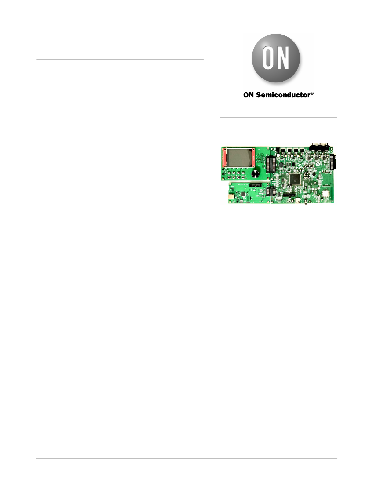
LC786830 Demo Board Kit comprises Main Board, LCD Board and
Downloader Board. The Main Board features miscellaneous
components to show the performance of LC786830. The LCD Board
has buttons as well as a LCD module for user interface.
Hardware
Main Board
• LC786830
• Power Supply
• Memory
• Bluetooth on Board Module
• Audio
• Interfaces
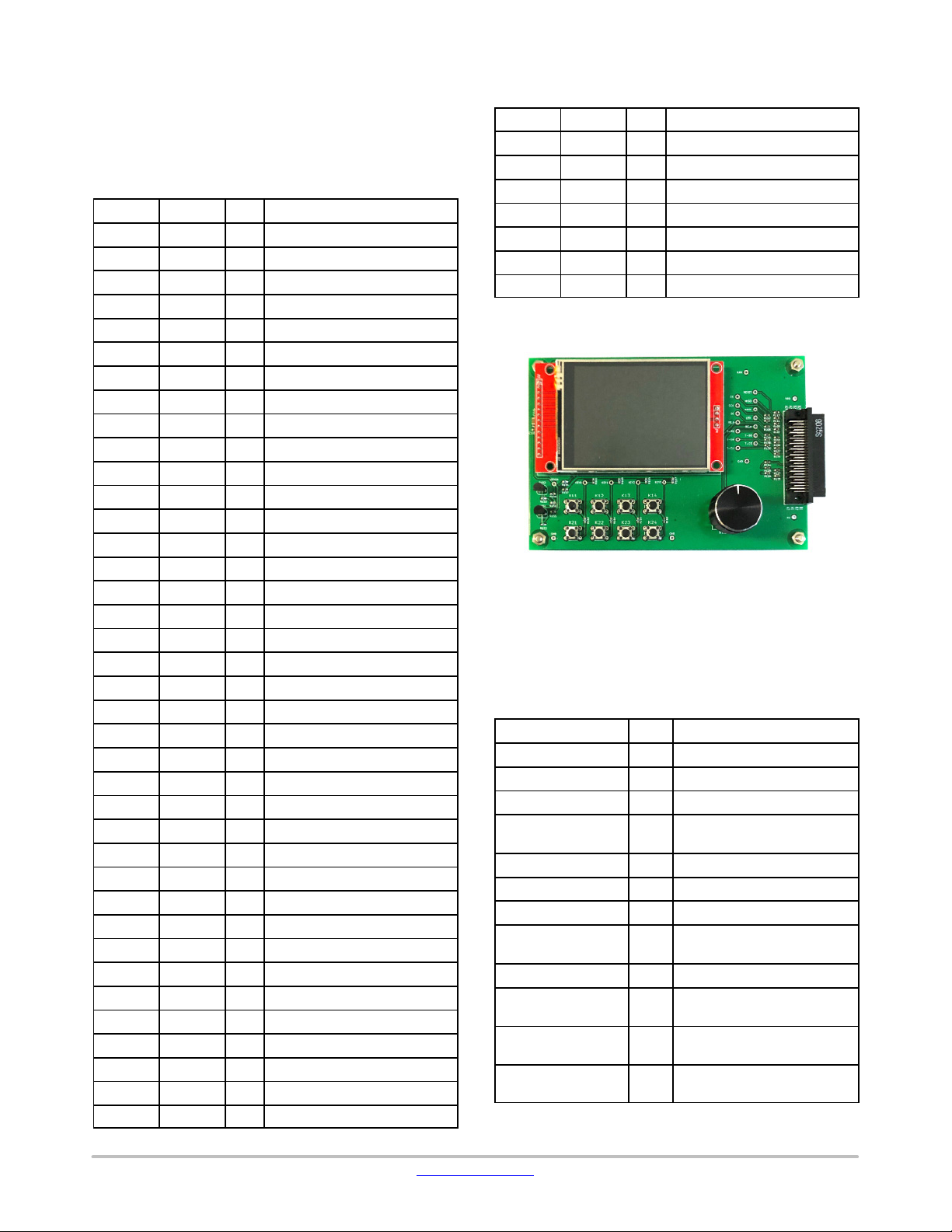
LCD Board
• LCD Module
• Key Button (2 x 4)
Downloader Board
• Microcontroller
• USB Type−B Connector
audio, and hands−free communication.
♦ 12 V/4 A DC Jack (2.1 mm center positive)
♦ LDO 1.2 V/3.3 V/5.0 V/8.0 V
♦ 16 Mbit QSPI Flash
♦ 32 Mbit QSPI Flash
♦ 256 kbit EEPROM
♦ 64 Mbit PSRAM (optional)
♦ ECM with Op Amp
♦ External DAC (Fs: 192 kHz)
♦ Piezo Speaker
♦ RCA Jack
♦ 3.5 mm Phone Jack
♦ USB Type−A Connector
♦ SD Card Socket (on the solder side)
♦ IR Receiver
♦ Debug
♦ JTAG 20−Pin Connector (SWD)
♦ Rotary Encoder
www.onsemi.com
EVAL BOARD USER’S MANUAL
LCD Board Main Board
Downloader Board
Figure 1. LC786830 Demo Board Kit
Semiconductor Components Industries, LLC, 2020
January, 2021 − Rev. 1
1 Publication Order Number:
EVBUM2769/D
Page 2
EVBUM2769/D
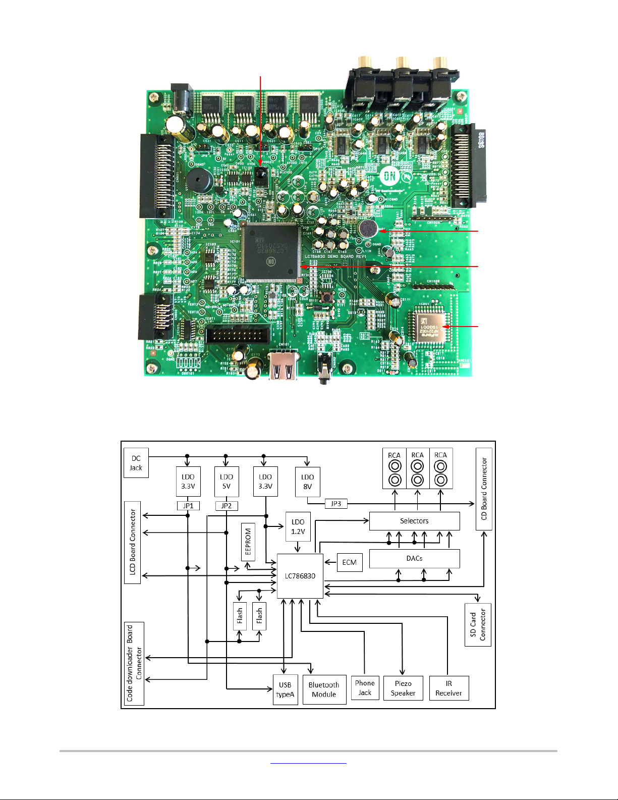
LCD Board
Connector
Downloader
Board
Connector
12 V DC Jack
IR Receiver
CD Board
Connector
ECM
LC786830
Bluetooth
Module
Phone Jack
Figure 2. LC786830 Demo Main Board
Figure 3. Block Diagram of LC786830 Demo Main Board
www.onsemi.com
2
Page 3
EVBUM2769/D
Power Supply
The enable pins of three LDOs on the Main Board are
connected to pins of LC786830 via jumpers. Thus, place
shunt jumpers on pins 2 and 3 of JP1, JP2 and JP3 before
powering the Main Board except when each state can be set
by GPs. Refer to the following table and figure. After that,
connect the plug of a 12 V power supply to the DC jack
(CN501, center positive, up to 4 A).
Table 1. JPS OF POWER SOURCE
Jumper Name Function Jumper Pin # State
JP1 Enable 3.3 V
(DVDD2)
JP2 Enable 5 V
(5V)
JP3 Enable 8 V
(CDV)
Figure 4. The Locations of JPs
Programing the Flash on the Board
1 GP00_1
3 ON
1 GP00_2
3 ON
1 GP00_0
3 ON
JP2
JP1
JP3
The Flash Writer Application can program the flash
memory on the Main Board from your PC over the
Downloader Board. The Flash Write Application is
available from the onsemi.com website.
Applications
Bluetooth module NF2210EZ is embedded on the Main
Board with printed antenna so that it is easy to establish a
Bluetooth connection with a phone or other device. An
electret condenser microphone is also embedded on the
Board for hands−free communication. It has a gain of 40 dB.
If you do not achieve that in your environment, please
replace resistors, R662 and R665 to adjust the gain.
Although the built−in DAC of the LC786830 supports up to
96 kHz sampling rates, external DACs which can accept
192 kHz sampling rates also are featured on the Board so
that 192 kHz sampling rates playback is acceptable. When
the output level of GP04_4 is low, built−in DAC outputs are
connected with RCA jack. When the output level of GP04_4
is high, external DAC outputs are connected with RCA jack.
Refer to the schematic of the Main Board. The 3.5 mm phone
jack is connected to a differential input on the LC786830 to
accept an analog input. The Main Board also has an
EEPROM for backup applications such as storing volume
settings. The SD Card socket is embedded on the solder side
as well. The Main Board can mount PSRAM but the
PSRAM needs to use same ports of LC786830 as the SD
Card control. Therefore, when PSRAM is available, the SD
Card solution is not available. In addition to that, there are
a piezo speaker and an IR receiver on the Main Board for
applications. Furthermore, the Main Board can be connected
with ON Semiconductor’s CD playback Board so that it is
easy to support a CD solution. A dedicated IIC interface is
available for MFi, via a CN102A terminal on the Main
Board.
For details of each component on the Boards, refer to its
datasheet.
Debugging
A Serial Wire Debug interface is available for debugging.
CN103 (JTAG 20−pin connector) on the Main Board is its
adaptor connector.
M0+ Code File
Process Indicator (%)
Figure 5. Flash Writer Application
Figure 6. Connect the Downloader Board to your PC
www.onsemi.com
Table 2. CN103 PIN ASSIGNMENT
CN103 Pin# Name Function
7 SWDIO SWD data I/O
9 SWCLK SWD clock
1, 2 3.3 V Power
4, 6, 8, 10, 12, 14,
16, 18, 20
Figure 7. Debugger Connected with CN103
GND Ground
Also, TP108 (TX0), TP109 (RX0), are prepared for
UART data logger monitor use in debugging.
3
Page 4
EVBUM2769/D
DSP Port Assignment
The General Ports of LC786830 are assigned according to
the table shown below. Refer to the table and schematics,
when developing application software.
Table 3. GP ASSIGNMENT TABLE
Name Function I/O Usage
GP00_0 GPIO O Enable 8 V (CDV)
GP00_1 GPIO O Enable 3.3 V (DVDD2)
GP00_2 GPIO O Enable 5 V (5V)
GP00_3 IRQ I Detect KEY0 input
GP00_4 IRQ I CD (mechanical−sw1)
GP00_5 IRQ I CD (mechanical−sw2)
GP00_6 IRQ I DISPLAY (T−IRQ)
GP00_7 TIMER I IR Receiver
GP01_0 IIC O EEPROM SCL
GP01_1 IIC I/O EEPROM SDA
GP01_2 GPIO O CD (S/L selector)
GP01_3 TIMER O Piezo Speaker
GP01_4 GPIO O CD (Driver Mute/active low)
GP01_5 GPIO O CD (Loader plus)
GP01_6 GPIO O CD (Loader minus)
GP01_7 GPIO I −
GP02_0 GPIO O USB (VBUS Disable/active low)
GP02_1 GPIO I USB (Detect Over Current)
GP02_2 GPIO O DISPLAY (T−CE)
GP02_3 SIO O DISPLAY (T−DIN)
GP02_4 SIO O DISPLAY (T−CLK)
GP02_5 SIO I DISPLAY (T−DO)
GP02_6 UART O Debug (M0+ TX)
GP02_7 UART I Debug (M0+ RX)
GP03_0 GPIO O DISPLAY (Enable LCD−Power)
GP03_1 GPIO O DISPLAY (LCD−CE)
GP03_2 GPIO O DISPLAY (LCD−RESET)
GP03_3 GPIO O DISPLAY (LCD−D/C)
GP03_4 SIO O DISPLAY (LCD−CLK)
GP03_5 SIO I DISPLAY (LCD−DO)
GP03_6 SIO O DISPLAY (LCD−DIN)
GP04_2 GPIO I Rotary−Encoder A
GP04_3 GPIO I Rotary−Encoder B
GP04_4 GPIO O Select Built−in/External DACs
GP04_5 GPIO I −
GP04_6 GPIO I −
GP04_7 GPIO I −
GP05_0 A/D I KEY0 input
Table 3. GP ASSIGNMENT TABLE (continued)
Name
GP05_1 A/D I KEY1 input
GP05_2 A/D I KEY2 input
GP05_3 A/D I KEY3 input
GP05_4 GPIO I −
GP05_5 GPIO I −
GP05_6 GPIO I −
GP05_7 GPIO I −
Function I/O Usage
LCD Board
Figure 8.
LCD module is mounted on the LCD Board.
Refer to the following table for a description of the signal
names. For more information about the components of the
LCD module, refer to their respective datasheets.
Table 4. LCD MODULE SIGNALS
Signal Name I/O Description
LED I Enable backlight
CS I Module CS, active low
RESET I Module Reset, active low
D/C I High: transmit data
MOSI I SPI Master Out Slave In
MISO O SPI Master In Slave Out
SCK I SPI clock
T−IRQ O Touch module,
T−CS I Touch module CS, active low
T−DIN I Touch module
T−DO O Touch module
T−CLK I Touch module
Low: transmit command
Touch detector, active low
SPI Master Out Slave In
SPI Master In Slave Out
SPI clock
www.onsemi.com
4
Page 5
Downloader Board
EVBUM2769/D
The microcontroller on the Board supports programing of
the flash on the Main Board from your PC. Place shunt
jumpers on pins 2 and 3 of JP101 and turn all switches of
DSW1 off. Reset switch, TSW1 controls the reset status of
the Microcontroller. The reset is active low. With the
Downloader Board connected to the Main Board, TSW1
must be turned to L (low) when debugging.
Figure 9.
LAYOUT
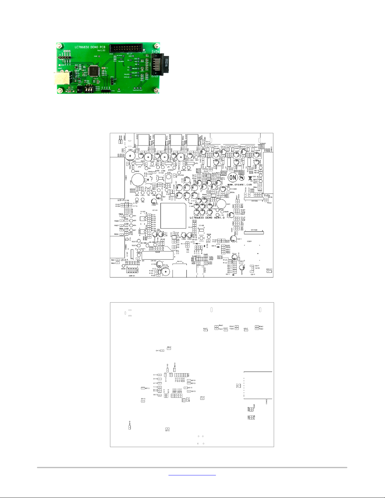
Figure 10. Layout of the Main Board of LC786830 Demo Board Kit (Top View)
Figure 11. Layout of the Main Board of LC786830 Demo Board Kit (Bottom View)
www.onsemi.com
5
Page 6
EVBUM2769/D
SCHEMATICS AND BILL OF MATERIALS
7
VCC
HLDB
CSB
7
VCC
HLDB
CSB1DO2WPB
DGND
RE−B
GP04−2
GP04−3
4 5
3
2
1
DVDD
6DI5
3
6DI5
3
GP05−AD0
KEY0
TEST0
C184 0.1
DGND
20
2
4
6
8
10
12
14
16
18
G
Vsply
Vtref
nTRST
CN103
1
3
OPEN
CLK
WPB
GND
W25Q32JVSSIQ
4
CLK
R194 4.7K
GND
W25Q16JVSSIQ
4
C183 OPEN
OPEN
C182
OPEN
C181
C180 OPEN
1000pF
C179
1000pF
C178
1000pF
C177
C176 1000pF
P104
P103
P102
33K
R109
R107 33K
GP05−AD3
GP04−4
GP05−AD1
GP05−AD2
KEY1
KEY2
KEY3
DACSEL
GP04−4
GP05−AD3
GP05−AD2
GP05−AD1
GP05−AD0
TP117
TP116 TEST0
TEST1
TEST2
TEST3
DGND
G
G
G
G
G
G
G
G
TDI
TMS
TCK
RTCK
TDO
nSRST
RQ
ACK
SWD
5
7
9
11
13
15
17
19
SWCLK
SWDIO
100
100
R168
R167
R166
R165 OPEN
M0−SWDIO
M0−SWCLK
TP120
TP121
DGND
0.1
C195
C194 0.1
C564
100u/10v
C120 0.1
C119 0.1
C563 100u/10v
0.1
C118
C117
0.1
0.1
C116
C115 0.1
C114 0.1
5V
IC107
SL:Low A
R140 10K
R139
10K
R138
10K
10K
R137
GP04−0
M3−SWCLK
C143 0.1
15
16
Vcc
OEB
SL
11A21B31Y42A52B62Y7
DGND
GP05−AD5
GP05−AD6
GP05−AD7
GP05−AD4
GP05−AD7
GP05−AD4
GP05−AD5
GP05−AD6
R142
10K
DVDD
GP04−1
GP07−7
M3−SWDIO
TEST3
TEST2
uC−TEST2
uC−TEST3
uC−MDCTL
uC−TEST1
uC−TEST0
TEST2
TEST3
TP118
TP119
93B103A114Y124B134A14
3Y
GND
74FST3257
8
DGND DGND
R141 10K
DGND
CN102B
WL−8DGND
1234567
8
0
R158
R159 OPEN
CN102A
8
VDD
CEB
IC105
1
CD−DI
CD−DO
CD−CL
CD−CE
SBCKO
PWI
SFSYI
SBSYI
OPCDM
CD−LRCK
CD−BCK
CD−DATA
CD−BUSYB
CD−RESB
P120
CP−SCL
CP−SDA
P122
P123
1234567
R154 10K
R155
R156
7
6
5
SCLK
SIO[3]
SI/SIO[0]
VSS
SO/SIO[1]2SIO[2]
3
4
IC101
LC786830
157
158
159
160
161
162
163
164
165
166
167
168
169
170
171
172
173
174
175
176
177
178
179
180
181
182
183
184
185
186
187
188
189
190
191
192
193
194
195
196
197
198
199
200
201
202
203
204
205
206
207
208
DGND
SDA
SCL
WL−8
8
2.2K
R157
DGND
C196 0.1
DGND
IPS6404L−SQ−SPN
Not mounted
DGND
0.1
0.1
C131
C132
C566 OPEN(100u/10v)
155
154
156
153
DVSS
DVDD
GP10_0
GP10_1
GP10_2
GP10_3
GP10_4
GP10_5
GP10_6
GP10_7
GP11_0
GP11_1
GP11_2
GP11_3
GP11_4
GP11_5
GP11_6
GP11_7
DVDD12
DVSS
DVDD
GP12_0
GP12_1
GP12_2
GP12_3
GP12_4
GP12_5
GP13_0
GP13_1
GP13_2
GP13_3
GP13_4
GP13_5
GP13_6
GP13_7
DVDD12
DVSS
DVDD
GP14_0
GP14_1
GP14_2
GP14_3
RESB
L1IN
R1IN
L2IN
R2IN
L3INP
L3INN
R3INP
R3INN
L4INP
L4INN
R4INP
R4INN
MICINP
AVDD12AVSS11AVDD27AVSS2
3
4
10u/50v
10u/50v
C162
C161
MICINP
0.1
OPEN(100u/25v)
C101
C151
C152 47u/50v
DVDD2
2.2K
2.2K
DVDD2
DVDD2
HCI−RESB
PCM_OUT
PCM_IN
PCM_CLK
PCM_SYNC
SDDET
SDWP
SDDAT2
SDDAT3
SDCMD
SDCLK
SDDAT0
SDDAT1
0
R118
0
R119
0
R120
0
R121
0
R122
R123
HCI_SCL
BUSYB
CD BUS
C561
C562
0
OUTPUT
INPUT
10u/50v
10u/50v
10u/50v
10u/50v
OPEN(10u/50v)
OPEN(10u/50v)
C168
C169
C170
C164
C163
C167
L1IN
R1IN
RESB
L3INP
R3INP
L3INN
R3INN
TP115
TP114
CD−SW1
CD−SW2
S/L
DMUTEB
LM+
LM−
DGND DGND
2.2K
R161
2.2K
HCI_SDA
R162
DVDD2
0.1
C133
C134 0.1
30_RTS
30_CTS
30_RX
30_TX
DVDD2
R163
OPEN
R164 OPEN
C135 0.1
C136 0.1
100u/10v
100u/10v
DVDD
AVDD
DVDD1.2V
220pF
OPEN(100u/10v)
C140
C565
P119
151
152
AFILT1
GP09_7
DVDD12
VREF_ADC
MICINN
5
6
VREF_ADC
MICINN
0.1
C102
5V
150
0.1
C103
GP09_6
149
GP09_5
DACOUT1L
8
DACOUT1L
100u/25v
C153
CN101
4700pF
C139
R117 1.5K
1K
R115
147
148
GP09_3
GP09_4
DACOUT1R9DACOUT2L
DACOUT1R
VBUS
1D−2D+3
UDP1
TEST3
146
145
144
UDP1
TEST3
GP09_2
DACOUT2R13DACOUT_S16VREF_DAC17AVDD311AVSS310AVDD415AVSS4
12
DACOUT2L
DACOUT2R
0.1
C104
C154 OPEN(100u/25v)
4
UDM1
143ID141
14
GND
0.1
C130
142
UDM1
UVDD1
0.1
C105
USB TYPE A
DGND
5V
C129 0.1
2.2K
R116
140
139
VBUS
UVSS1
18
DACOUTS
VREF_DAC
OPEN(100u/25v)
47u/50v
0.1
C155
C156
C106
5V
220u/25v
C173
4
6
5
FLG
OUT
ILIM
IN
GND2EN
IC106
NCV380H(UDFN6)
1
3
0.1
DGND
C171
C172 100u/25v
DVDD2
0.1
0.1
C128
C124
C127 0.1
270
TEST2
R114
6pF
6pF
24MHz
C126
C125
P117
P118
X102
R113 220
129
130
131
138
132
133
134
135
136
137
UDP2
XVSS
UDM2
XVDD
RBIAS
TEST2
UVDD2
X24MIN
UVDD12
X24MOUT
TEST020TEST1
GP00_022GP00_123GP00_224GP00_325GP00_432GP00_533GP00_634GP00_7
AVDD519AVSS5
21
0
INT0
R101
X101
KEY0−ACK
Enable DVDD2
18pF
Enable 5V
TP102
C109
32.768kHz
0.1
C108
GP00−3
GP00−2
GP00−1
GP00−0
TP103
OPEN(100u/25v)
0.1
C157
C107
AGND
10K
0.1
DVDD2
C141
DGND
R131
1
2
3
Vcc
GND
VOUT
IRC
U101
DGND
R153 5.49K(0.1%)
DGND
R151 10K
R152 10K
OVCRB
VBUSCUTB
M3TX
C123 0.1
P115
P109
P110
P111
P112
P113
P114
P116
119
120
121
122
123
124
125
126
128
127
UVSS2
GP08_5
GP08_2
GP08_3
GP08_4
GP08_6
GP08_7
GP09_0
GP09_1
DVDD12
LC786830
DVDD30XVSS1229XVDD1226X32KIN27X32KOUT28MODE
GP01_036GP01_137GP01_238GP01_3
31
35
T−IRQ
18pF
S/L
EPSDA
EPSCL
IRC
CD−SW1
CD−SW2
C110
C111 0.1
GP00−6
IR
R132 20K
DGND
R134 2.2K
R133
2.2K
7
8
6
5
WP
0.1
Vcc
DGND
SCL
SDA
A0
VSS
IC102
C142
1A12A23
4
DGND
CD−RESB
CD−RESB
PUIN
C121 0.1
C122 0.1
P108
117
118
114
116
115
DVSS
DVDD
GP08_0
GP08_1
DVDD12
GP01_440GP01_541GP01_645GP01_7
DVDD12
43
39
42
BEEP
DMUTEB
LM+
PWM
C112 0.1
TP104
1K
R135
5V
CAT24C256
DGND
CD−BUSYB
6800pF
C138
R112 2.2K
113
0.1
C113
CD−BUSYB
AFILT2
DVDD44DVSS
CD−LRCK
CD−LRCK
112
GP07_7
LM−
SBSYI
CD−BCK
CD−DATA
OPCDM
CD−BCK
CD−DATA
OPCDM
SBSYI
220pF
C137
P107
077
22
R111
108
109
110
111
GP07_5
GP07_6
M3 SWDT
M3 SWCK
GP02_047GP02_148GP02_249GP02_350GP02_451GP02_5
46
TM
OVCRB
VBUSCUTB
TP105
T−CS
GP02−2
1
2
U102
SFSYI
PWI
SFSYI
106
107
GP07_4
I2CL
TP106
R102 0
T−CLK
T−DIN
GP02−3
PiezoSpeaker
PWI
GP07_3
GP02−4
D101 GMA01
R136 1K
SBCKO
105
52
I2DA
TP107
0
R103
T−DO
SBCKO
GP07_2
GP02−5
LM−
S/L
DMUTEB
CD−SW1
CD−SW2
PUIN
CD−DO
CD−CE
CD−DI
CD−CL
LM+
CD−DI
CD−DO
CD−CL
CD−CE
DMUTEB
LM−
S/L
CD−SW1
CD−SW2
PUIN
LM+
DVDD
DAC−DATA
DAC−BCK
DAC−LRCK
DAC−DATAR
DAC−DATAS
GP07−4
GP07−0
GP07−1
GP07−2
GP07−3
8
4.7K
P105
P106
R195
IC104
1DO2
8
47
GP07_1
104
R180 47
R18147R182
GP07_0
103
SFLDI2
102
SFLCL2
101
SFLHOLD2
SFLCS2
SFLDO2
SFLWP2
DVDD
DVSS
DVDD12
SFLDI1
SFLCL1
SFLHOLD1
SFLCS1
SFLDO1
SFLWP1
GP04_1
GP04_0
DVSS
DVDD
GP05_7 / AD7
GP05_6 / AD6
GP05_5 / AD5
GP05_4 / AD4
DVDD
DVSS
DVDD12
GP05_3 / AD3
GP05_2 / AD2
GP05_1 / AD1
GP05_0 / AD0
GP04_7
GP04_6
GP04_5
GP04_4
GP04_3
GP04_2
M0 SWCK
M0 SWDT
GP03_6
GP03_5
DVDD
DVSS
DVDD12
GP03_4
GP03_3
GP03_2
GP03_1
GP03_0
GP02_7
GP02_6
OPEN
OPEN
R104
R105
Q101
PN2222
123
IC103
100
99
47
R179
R178
98
47
97
47
R177
96
95
94
R176
93
47
R175
92
47
R174
91
47
R173
90
47
89
47
R172
88
R171 47
87
86
85
84
GP05−AD7
83
GP05−AD6
82
GP05−AD5
81
GP05−AD4
80
79
78
77
GP05−AD3
76
GP05−AD2
75
GP05−AD1
74
GP05−AD0
73
GP04−4
72
71
0.01
C175
70
0.01
C174
69
1K
R110
68
R108
1K
67
66
R106 22
65
64
63
62
61
60
59
58
57
56
55
54
53
TX0
RX0
RE−A
LEDCSRESET
D/C
SCK
MISO
MOSI
TP108
TP109
M0TX
GP03−0
GP03−3
GP03−6
GP03−4
GP03−5
GP03−1
GP03−2
TEST1
TEST1
TEST0
DGND
DSW101
SW−DIP4
Not mounted
6
DVDD2
7
8
Figure 12. LC786830 DEMO (Main Board)
www.onsemi.com
6
Page 7

3.3V IN
DVDD
6EN5
7
8
NC
Vcc
Vo
Vo_s
IC504 BD12IC0MEFJ
1
2
3NC4
R541 0
TP512 D1.2V
DVDD1.2V
EVBUM2769/D
C542 1uF
NC
G
9
DGND
GND
C541 1uF
DGND DGND DGND
TP513 DGND TP514 DGND
DGND
CDV
R557 0 TP515 CDV
4
VOUT
NCP59302
VIN
IC505
2
47K
R5530R555
R554
5
ADJ
GND
3
GND
EN
1
0.1
GP00−0
DVDD
AVDD
JP3
1 3
NCP59302
IC501
243
TP506 DVDD
0
R517
4
VOUT
VIN
2
Power
TP501
0
R501
AVDD
TP507
R518 0
5
1
C513 220u/25v
10K
3.3K
R513
R514
ADJ
GND
3
GND
EN
0.1
GND
1.2K
6.8K
R515
R516
GND
47K
OPEN
R511
R512
C512
C511 10u/50v
GND
AGND
DGND
MICGND
DGNDR504 0
MICGND
TP503
TP505
TP504 AGND
0
0
R505
R506
GND
TP502
C501 1000u/25v
0
R502
0
R500
DVDD
2
1.8K
6.8K
R556
GND
OPEN
10K
R551
R552
C552
C551 10u/50v
GND
AVDD2
DVDD2
MICVDD
DVDD2
MICVDD
TP509 AVDD2
TP508
TP510
0
0
R529
R528 0
R527
3.3K
R523
4
5
ADJ
VOUT
GND
3
NCP59302
EN
VIN
IC502
1
2
0.1
GND
DVDD
C523 220u/25v
10K
1.2K
6.8K
R525
R526
R524
GND
OPEN
10K
R521
R522
C522
C521 10u/50v
GP00−1
5V
JP1
1 3
2
TP511 5V
0
R537
GND
GND
GND
4
VOUT
NCP59302
VIN
IC503
2
2.2K
R533
5
ADJ
GND
3
EN
1
0.1
DVDD
C533 220u/25v
33K
4.7K
6.8K
R535
R536
R534
GND
OPEN
10K
R531
R532
C532
C531 10u/50v
GP00−2
JP2
1 3
2
GND
GND
GND
DVDD
RESB
100 TP101 RESB12
R191
SW101
TACT
RESET
12
34
D192 GMA01
1uF
C191
R192 18K
1uF
C192
1uF
C193
DGND
D191
uC−RESB
CN501
DC JACK
Figure 13. LC786830 DEMO (Main Board) − POWER & RESET
www.onsemi.com
7
Page 8

EVBUM2769/D
DVDD2
GP07−0
GP07−1
GP07−0
GP07−1
GP07−2
DAC−DATA
DAC−BCK
DAC−LRCK
10K
OPEN
R605
R606
16
18
FLT
MODE117MODE2
ATT211ATT112ATT013MAST
DEMP
2200pF
R603
1
B1
IC605
6
C605
0.1
C604
DOUT
10u/50V
470
15
AGNS
14
2B03
GND
DGND
PCM5142
AGND
1uF
A4Vcc5Select
C613
NLASB3157DFT2G
DGND
AGND
DVDD2
10u/50V
C629
AVDD2
AVDD2
DVDD2
DGND
10u/50V
0.1
10u/50V
0.1
C609
C608
C606
C607
0
R608
19
20
21
22
23
24
25
26
28
DIN
SCK
BCK
FMT
LRCK
LDOO
XSMT
DGND27DVDD
CAPM4VNEG5OUTL6OUTR
AGND
CPVDD
CAPP2CPGND
IC601
AVDD2
AVDD2
AVD D
1
3
7
8
9
10
2.2uF
C603
2.2uF
0.1
C602
C601
AGND
AVDD2
2200pF
470
R602
C610
C611
AGND
1
2B03
B1
1uF
GND
A4Vcc5Select
NLASB3157DFT2G
C612
IC604
6
AVDD2
GP07−3
DAC−DATAR
DAC−BCK
DAC−LRCK
10K
OPEN
R625
R626
18
2200pF
IC607
ATT211ATT1
R623
DGND
DGND
C649 10u/50V
DVDD2
15
16
AGNS
DOUT
MODE117MODE2
ATT013MAST
PCM5142
12
14
10u/50V
C625
0.1
C624
AGND
470
1
2B03
B1
GND
A4Vcc5Select
6
1uF
C615
NLASB3157DFT2G
AVDD2
AGND
AVDD2
DVDD2
DGND
0.1
0.1
C628
C626 10u/50V
C627
0
R628
19
20
21
22
23
24
25
26
28
DIN
FLT
SCK
BCK
FMT
LRCK
LDOO
XSMT
DGND27DVDD
AGND
CPVDD1CAPP
CAPM4VNEG5OUTL
DEMP
CPGND
OUTR7AVD D
IC602
2
3
6
8
9
10
2.2uF
C623
2.2uF
0.1
C622
C621
AGND
AVDD2
2200pF
470
R622
C630
C631
AGND
1
2B03
B1
GND
A4Vcc5Select
NLASB3157DFT2G
C614 1uF
IC606
6
AVDD2
GP07−4
GP07−0
GP07−1
DAC−DATAS
DAC−BCK
DAC−LRCK
10K
OPEN
R645
R646
FLT
DEMP
2200pF
DGND
DGND
15
16
18
AGNS
DOUT
MODE117MODE2
ATT2
MAST
ATT112ATT0
PCM5142
11
13
14
10u/50V
C645
0.1
C644
AGND
470
R643
1
2B03
B1
1uF
GND
A4Vcc5Select
C617
NLASB3157DFT2G
IC609
6
DACOUT1L
C673
R673
AGND
10u/50v
680
DACOUT1R
DACOUT2L
C674
10u/50v
C677
AGND
R677
680
680
R674
1000pF
C671
1000pF
C672
R671
100K
R672
100K
10u/50v
DACOUT2R
DACOUTS
C678
10u/50v
AGND
680
R678
1000pF
C675
1000pF
C676
R675
100K
R676
100K
10u/50v
C680
AGND
680
R680
1000pF
C679
100K
R679
GP04−4
10K
R691
DGND
DVDD2
DGND
10u/50V
0.1
C648 0.1
C646
C647
0
R648
19
20
21
22
23
24
25
26
28
DIN
SCK
BCK
FMT
LRCK
LDOO
XSMT
DGND27DVDD
CPVDD
CAPM4VNEG5OUTL6OUTR7AVD D
AGND
CAPP2CPGND
IC603
1
3
8
9
10
2.2uF
C643
2.2uF
0.1
C642
C641
AGND
AVDD2
2200pF
470
R642
C650
C651
AGND
1
2B03
B1
1uF
GND
A4Vcc5Select
NLASB3157DFT2G
C616
IC608
6
AVDD2
CN601
AGND
1
2
Lch(W)
3
GND
Rch(R)
OUT
U601
2
C662 100u/10v
MICGND
C661
0.1
C666 100pF
R665 100K
R661 2.2K
R662 1K C663 10uF
R663 10KR664 10K
4V+5
−IN
+IN
OUT
IC610
1V−2
3
0
R666
MICINP
MICVDD
GND
1
OPA344NA
5
Lch(W)
ECM
AGND
4
6
GND
Rch(R)
C664 1uF
MICGND
C665 0.1
R667 0
MICINN
R681
R684
0
R688
R3INP
0
C681
OPEN
R6850R686
OPEN
R3INN
CN602
C682
AGND
7
8
Lch(W)
AUX JACK
324
R682
OPEN
0
R689
OPEN
L3INN
9
GND
Rch(R)
RCJ−61232323
0R687
R683 OPEN
GND
C683 OPEN
GND
0
L3INP
Figure 14. LC786830 DEMO (Main Board) − AUDIO IN/OUT
www.onsemi.com
8
Page 9

DVDD2
EVBUM2769/D
HCI_SDA
HCI_SCL
PCM_OUT
PCM_IN
PCM_CLK
PCM_SYNC
0.1
GND
GND
GND
GND
C216
C214
SPI_MISO
SPI_MOSI
SPI_CLK
SPI_CS#
DGND
DGND
26
VDD_S_3V3
RF IN/OUT
33
DGND
D212
1KR214 0 21
R225
SCL
10u/50v
24
25
VDD_PADS
VDD_S_3V3
GND34GND35GND
GND
36
OPEN
SDA
PIO_420PIO_5
PIO_221PIO_122PIO_323PIO_0
NF2210EZ
GND
GND2GND3RESETB4GND5UART_CTS
1
DGND
17
18
19
OPEN
10K
R222
GND
6
RTS
PCM_OUT
PCM_IN
16
PCM_SYNC
15
PCM_CLK
14
PCM/SPI_SELECT
13
USB_UARTB_SEL
12
USB_DP
11
USB_DN
10
UART_RTS
CTS
9
UART_TXD
TX
8
UART_RXD
7
RX
DGND
R221
R219
OPEN
10K
R220
DGND DGND
DN
DP
DN
DP
P211
P212
0
220
220
220
R231
R230 0
100u/25v
0
R224
C211
HCI3.3v
R229
DGND
R228
R227
1608 size
R226 220
C218
0 ohm
AMCA31
Chip Antenna (2450MHz)
C217
C219
OPEN
OPEN
10u/50v
C215
DGND
0.1
C213
PCM_OUT
PCM_IN
PCM_CLK
PCM_SYNC
1608 size
1608 size
IC201 NF2210EZDGND
DGND
27
28
29
30
31
32
37
38
39
40
RXTXCTS
R213 0
30_TX
0
R215
30_RX
RTS
0
R216
30_RTS
30_CTS
RTS
R218
21
D211
51K
GMA01
C212
0.1
DGND
1.8K
R217
HCI−RESB
RESB5VGNDRXGNDTXCTS
Figure 15. LC786830 DEMO (Main Board) − NF2210EZ BT RF Module
www.onsemi.com
9
Page 10

DVDD
EVBUM2769/D
10K
DVDD2
0
R463
CN401
DAT3/CS
DAT2/RSV
1
9
100
100
100
R471
R472
R470
GP04−1
GP04−0
GP07−7
M3−SWDIO
GP05−AD5
GP05−AD6
GP05−AD7
GP05−AD4
AD7
AD4
AD5
AD6
TP110
TP111
TP112
A1 B1
M0TX
OPEN
OPEN
OPEN
TP113
R828 OPEN
R827
R826
R825
FX2−20P−1.27DS
DGND
0
0
R8230R8220R821
R824
DGND
M3TX
CN802
A9 B9
A10 B10
A2 B2
A3 B3
A4 B4
A5 B5
A6 B6
A7 B7
A8 B8
DVDD2
47K
R469
47K
R468
47K
R467
47K
R466
47K
R465
10K
R464
0
0
R462
R461
R475
C465
C464 33pF
C463
C462
C461
100
R473
WriteProtect
8
100
R474
DGND
CMD/DI2VSS13VCC4CLK/SCLK5VSS26DAT0/DO7DAT1/RSV
33pF
33pF
33pF
33pF
SD Card
CardDetect
Common
C467 0.1
DGND
C466
100u/10v
CN803
DMUTEB
A1 B1
A2 B2
0
R862
DGND
BUSYB
PUIN
A8 B8
DGND
B9
A9
CD−Power
TP122
0
R870
uC−TEST2
B10
A10
M3−SWCLK
SBCKO
PWI
B12
B11
A11
A12
CD3.3v
TP123
OPEN
R872
uC−TEST3
SFSYI
B13
A13
OPEN
R877
uC−RESB
SBSYI
B14
A14
uC−MDCTL
CD−LRCK
B15
A15
CD5v
TP124
OPEN
R878
SDWP
SDDET
SDCLK
SDCMD
SDDAT1
SDDAT0
SDDAT3
SDDAT2
GP05−AD3
GP05−AD2
GP05−AD1
CD−BCK
CD−DATA
CD−BUSYB
OPCDM
CD−RESB
CD−DO
CD−CE
CD−DI
CD−CL
B16
B17
B18
B19
B20
B21
B22
B23
B24
B25
B26
FX2−52S−1.27DS
A16
A17
A18
A19
A20
A21
A22
A23
A24
A25
A26
5V
CN801
A1 B1
A2 B2
P801 AD5
GP05−AD0
KEY3
KEY0
KEY1
KEY2
DGND
B9
A3 B3
A4 B4
A5 B5
A6 B6
A7 B7
A8 B8
A9
P802 AD6
P803 AD4
P807 AD7
GP02−4
GP02−2
GP02−3
GP02−5
GP00−6
GP04−2
GP04−3
GP00−3
T−CLK
T−CS
T−DIN
T−DO
T−IRQ
RE−A
RE−B
KEY0−ACK
DVDD
10K
R801
DGND
DVDD2
B16
B15
B14
B13
B10
B12
B11
B17
B18
B19
A16
A10
A11
A17
A18
A15
A14
A13
A12
DGND
A19
DVDD2
DGND
B20
B21
B22
B23
B24
B25
B26
A20
A21
FX2−52P−1.27DS
A24
A25
A22
A23
A26
uC−TEST1
uC−TEST0
S/L
LM+
CD−SW1
CD−SW2
LM−
A3 B3
A4 B4
A5 B5
A6 B6
A7 B7
0
R864
GND
CDV
DVDD2
GP05−AD5
GP05−AD6
GP05−AD4
5V
GP05−AD7
LED
MOSI
SCK
D/C
MISOCSRESET
GP03−0
GP03−3
GP03−6
GP03−4
GP03−5
GP03−1
GP03−2
Figure 16. LC786830 DEMO (Main Board) − I/Fs & SD
www.onsemi.com
10
Page 11
EVBUM2769/D
Table 5. BILL OF MATERIALS FOR THE MAIN BOARD OF LC786830 DEMO BOARD KIT
Designator Value MFR MFG P/N Description
IC101 ON Semiconductor LC786830W
IC102 ON Semiconductor CAT24C256WI−GT3
IC103 Winbond W25Q16JVSSIQ For your application
IC104 Winbond W25Q32JVSSIQ Don’t overwrite.
IC105 IPUS IPS6404L−SQ−SPN Not mounted, PSRAM
IC106 ON Semiconductor NCP380HSNAJAAT1G
IC107 ON Semiconductor 74FST3257DR2G
IC201 nFore NF2210EZ (2.4 GHz, Stamp−40) Bluetooth module on
IC501, IC502, IC503, IC505 ON Semiconductor NCP59302DSADJR4G
IC504 Rohm BD12IC0MEFJ−ME2
IC601, IC602, IC603 TI PCM5142PWR
IC604, IC605, IC606, IC607,
IC608, IC609
IC610 TI OPA344NA/250
X101 NDK NX3215SA−32.768 kHz−STD−MUS−2
X102 NDK NX3225GA−24.000 MHz−STD−CRG−2
D191 ON Semiconductor 1N5819 Schottky Diode, 40 V, 1 A
D101, D192, D211 Sanyo GMA01U−BT
D212 − − Not mounted, LED
R101, R102, R103, R118,
R119, R120, R121, R122,
R123, R158, R213, R214,
R215, R216, R224, R230,
R231, R461, R462, R463,
R500, R501, R502, R504,
R505, R506, R517, R518,
R527, R528, R529, R537,
R541, R553, R557, R608,
R628, R648, R666, R667,
R681, R682, R684, R685,
R686, R687, R821, R862,
R864, R870, C218
R106, R111
R171, R172, R173, R174,
R175, R176, R177, R178,
R179, R180, R181, R182
R167, R168, R191, R470,
R471, R472, R473, R474
R113, R226, R227, R228,
R229
R602, R603, R622, R623,
R642, R643
R673, R674, R677, R678,
R680
R108, R110, R115, R135,
R136, R225, R662
R515, R525
R117
R217, R555
R133, R134, R161, R162,
R533, R112, R116, R155,
R156, R157, R661
0 W
22 W
47 W
100 W
220 W
470 W
680 W
1.0 kW
1.2 kW
1.5 kW
1.8 kW
2.2 kW
ON Semiconductor NLASB3157DFT2G
Rohm MCR03EZPJ000
Rohm MCR03EZPJ220
Rohm MCR03EZPJ470
Rohm MCR03EZPJ101
Rohm MCR03EZPJ221
Rohm MCR03EZPJ471
Rohm MCR03EZPJ681
Rohm MCR03EZPJ102
Rohm MCR03EZPJ122
Rohm MCR03EZPJ152
Rohm MCR03EZPJ182
Rohm MCR03EZPJ222
software.
Board
www.onsemi.com
11
Page 12

EVBUM2769/D
Table 5. BILL OF MATERIALS FOR THE MAIN BOARD OF LC786830 DEMO BOARD KIT (continued)
Designator DescriptionMFG P/NMFRValue
R513, R523
R535, R194, R195
R516, R526, R536, R556
R131, R137, R138, R139,
R140, R141, R142, R151,
R152, R154, R220, R222,
R464, R475, R514, R522,
R524, R532, R552, R605,
R625, R645, R663, R664,
R691, R801
R192
R132
R107, R109, R534
R465, R466, R467, R468,
R469, R511, R554
R218
R665, R671, R672, R675,
R676, R679
R114
R153
R104, R105, R159, R163,
R164, R165, R166, R219,
R221, R512, R521, R531,
R551, R606, R626, R646,
R683, R688, R689, R825,
R826, R827, R828, R872,
R877, R878
C125, C126 6 pF muRata GRM1882C1H6R0DZ01
C109, C110 18 pF muRata GRM1882C1H180JA01
C461, C462, C463, C464,
C465
C666 100 pF muRata GRM1882C1H101JA01
C137, C140 220 pF muRata GRM1882C1H221JA01
C176, C177, C178, C179,
C671, C672, C675, C676,
C679
C610, C611, C630, C631,
C650, C651
C139 4700 pF muRata GRM188B11H472KA01
C138 6800 pF muRata GRM188B11H682KA01
C174, C175
C101, C102, C103, C104,
C105, C106, C107, C108,
C111, C112, C113, C114,
C115, C116, C117, C118,
C119, C120, C121, C122,
C123, C124, C127, C128,
C129, C130, C131, C132,
C133, C134, C135, C136,
C141, C142, C143, C171,
C184, C194, C195, C196,
C212, C213, C214, C467,
C512, C522, C532, C552,
C601, C604, C607, C608,
C621, C624, C627, C628,
C641, C644, C647, C648,
C661, C665
3.3 kW
4.7 kW
6.8 kW
10 kW
18 kW
20 kW
33 kW
47 kW
51 kW
100 kW
270 W
5.49 kW
Not mounted − Not mounted, Resistor
33 pF muRata GRM1882C1H330JA01
1000 pF muRata GRM1882C1H102JA01
2200 pF muRata GRM188B11H222KA01
0.01 mF
0.1 mF
Rohm MCR03EZPJ332
Rohm MCR03EZPJ472
Rohm MCR03EZPJ682
Rohm MCR03EZPJ103
Rohm MCR03EZPJ183
Rohm MCR03EZPJ203
Rohm MCR03EZPJ333
Rohm MCR03EZPJ473
Rohm MCR03EZPJ513
Rohm MCR03EZPJ104
Susumu RR0816P−271−D
Susumu RG2012P−5491−B−T5
muRata GRM188R71C103KA01D
muRata GRM188R71C104KA01D
www.onsemi.com
12
Page 13

EVBUM2769/D
Table 5. BILL OF MATERIALS FOR THE MAIN BOARD OF LC786830 DEMO BOARD KIT (continued)
Designator DescriptionMFG P/NMFRValue
C191, C192, C193, C664,
C541, C542, C612, C613,
C614, C615, C616, C617
C602, C603, C622, C623,
C642, C643
C663
C180, C181, C182, C183,
C217, C219, C681, C682,
C683
C605, C606, C609, C625,
C626, C629, C645, C646,
C649, C161, C162, C167,
C168, C169, C170, C215,
C216, C511, C521, C531,
C551, C673, C674, C677,
C678, C680
C152, C156
C153, C172, C211
C466, C561, C562, C563,
C564, C662
C173, C513, C523, C533
C501
C151, C154, C155, C157,
C163, C164, C565, C566
JP1, JP2, JP3 Mac8 WL−8
DSW101 OTAX KSD42 Not mounted, DIP−SW
SW101 Alps Alpine SKHHAJA010
U101 Sanyo SPS−440−1
U102 muRata PKM13EPYH4000−A0
U601 DB Products Limited C9767BB422LFP
AMCA31 ABRACON AMCA31−2R450G−S1F−T3
CN101 Omron XM7A−0442
CN102A, CN102B Mac8 WL−8
CN103 HIROSE HIF3FC−20PA−2.54DSA (71)
CN401 YAMAICHI FPS009−2406−0
CN601 CUI Inc. RCJ−61232323
CN602 SWITRONIC ST−005−G
CN801 HIROSE FX2−52P−1.27DS (71)
CN802 HIROSE FX2−20P−1.27DS (71)
CN803 HIROSE FX2−52S−1.27DS (71)
1 mF
2.2 mF
10 mF
Not mounted − − Not mounted, Ceramic
10 mF/50 V
47 mF/25 V
100 mF/25 V
100 mF/10 V
220 mF/25 V
1000 mF/25 V
Not mounted − − Not mounted,
muRata GRM188R71C105KA12D
TDK C1608X7S0J225K080AB
muRata GRM188D71A106MA73D
Capacitor
Nichicon UKW1H100MDD1TD
Nichicon UKW1E470MDD1TD
Nichicon UKW1E101MED1TD
suncon 10ME100HC
Nichicon UKW1E221MPD1TD
Nichicon UKW1E102MPD1TD
Electrolytic Capacitor
www.onsemi.com
13
Page 14

TP102 DVDDTP101 DGND
DVDDDGND
KEY0
KEY3
KEY2
KEY1
KEY3
KEY2
KEY1
KEY0
5V
TP125
TP126
TP127
TP128
DGND
TP121 5V
R1250R1260R1270R1280R1350R1360R1370R1380R1390R1400R141
B9
B10
CN101
A1 B1
A2 B2
A3 B3
A4 B4
A5 B5
A6 B6
A7 B7
A8 B8
A9
A10
EVBUM2769/D
R_ENC
RE101
B
A
G
DGND
KEY0
T−CLK
T−CS
T−DIN
T−DO
T−IRQ
RE−A
RE−B
T−CS
T−DIN
T−DO
T−IRQ
RE−A
RE−B
TP135 T−CLK
TP137
TP138
TP139
TP140
TP141
TP136
0
B16
B17
B18
B19
A16
A17
A18
A19
R1070R1080R1090R1100R1110R1120R113
MOSI
TP107 LED
TP108 DC
TP109
LEDDCMOSI
0
DGND
R144
B20
B21
B22
B23
B24
B25
B26
FX2−52S−1.27DS
A20
A21
A22
A23
A24
A25
A26
0
RESET
SCK
MISO
CS
TP113
TP110
TP111
TP112
SCK
MISO
CS
RESET
SD_SCK
SD_CS
SD_MOSI
SD_MISO
CN103
WL−8−4
123
4
LED
KEY3
KEY2
KEY1
KEY0
DVDD
10k
10k
R167
R168
34
34
K14
TACT
K24
TACT
12
12
10k
10k
R165
R166
34
34
K13
TACT
K23
TACT
12
12
10k
10k
R163
R164
34
34
K12
TACT
K22
TACT
12
12
10k
10k
R162
R161
34
34
K11
TACT
K21
TACT
12
12
DGND
0V
1.65V
DGND
DVDD
B15
B14
B13
B12
B11
A15
A14
A13
A11
A12
DGND
DVDD
R157 0
DVDD
R156 OPEN
C104 100u/10v
DGND
C103 0.1z
DVDD
T−DIN
T−DO
DC
MOSI
SCK
MISO
CS
RESET
T−CLK
T−CS
T−IRQ
C102 100u/10v
DGND
C101 0.1z
CN102
TP178 LED−ON
1
2CS3
4
5
6
8
9
10
D/C
SCK7LED
VCC
GND
MOSI
MISO
RESET
DGND
11
12
13
14
T−CS
T−DO
T−IRQ
T−DIN
T−CLK
Socket−Pin14
0
R171
Figure 17. LC786830DEMO − LCD Board
www.onsemi.com
14
Q151
2SA733
312
R151 3k3
R153 3k3
R152 10k
DGND
10k
R154
Q152
2SC945
231
0
R155
DGND
Page 15

EVBUM2769/D
Table 6. BILL OF MATERIALS FOR THE LCD BOARD OF LC786830 DEMO BOARD KIT
Designator Value MFR MFG P/N Description
Q151 UNISONIC
Q152 UNISONIC
RE101 Alps EC12E2430803
LCD Module HiLetgo
K11, K12, K13, K14, K21,
K22, K23, K24
R107, R108, R109, R110,
R111, R112, R113, R125,
R126, R127, R128, R135,
R136, R137, R138, R139,
R140, R141, R144, R155,
R157, R171
R151, R153
R152, R154, R161, R162,
R163, R164, R165, R166,
R167, R168
R156 Not mounted − Not mounted, Resistor
CN101 HIROSE FX2−52S−1.27DS (71)
CN103 aitendo PH254S−B6−40P
0 W
3.3 kW
10 kW
TECHNOLOGIES
TECHNOLOGIES
Cosland TS−0606
KOA RK73Z1JTTD
KOA RK73H1JTTD3301F
KOA RK73H1JTTD1002F
2.8TFT LCD DISPLAY Touch Panel
SPI serial 240*320 ILI9341 5 V/3.3 V
2SA733
2SC945
www.onsemi.com
15
Page 16

DVDD
TSW1
RESET
D1
GMA01
R71
X1
PC4
SO0_DSPI
SI0_DSPO
1
456
220k
DVDD
12.0MHz
EVBUM2769/D
DVDD
TP2
DSW1
SW−DIP3
4
DVDD
5
6
GND
VBUS
USB
CN102
1D−2D+3
4
TP1
C6
5P
C5
5P
INT3
100
R66
45
47
48
INT246INT3
RES#
XT1/AN10
XT2/AN11
VSS1
CF1
CF2
VDD1
PC0
PC1
PC2
PC3
PC4
PC5
PC6
PC7
SO0
SCK0
SO12SI13SCK14P165P176PWM17PWM08VDD29VSS2
1
SCK0_CLK
SCK1
VBUS
42
43
AN844AN9
VSS3
P34/UFILT
P17
R67
1.5k
Q101
2SA1179N
312
DVDD
47k
R69
3
3.3k
R68
G−12
DGND
0
R70
1uk
C10
0
R73
100u/10v
220
R72
C8
OPEN
C9
2.2u/50v
C11
IC101
LC87F10C8A
49
50
51
52
53
0.1z
54
C14
55
56
57
58
59
60
61
62
63
SI0
64
33
33
R64
R65
C2 0.1z
D+
D−
39D−40D+41
LC87F10C8A
10
C1
0.1z
VB_ON
47k
R52
3
2
1
MODE2
MODE1
MODE0
38
VDD3
P0011P0112P0213P0314P0415P05
PB0_RES
R60
34
P3035P3136P3237P33
PB0
33k
R63
R62
33k
R61 33k
2.2k
33
PB1
16
DGND
IC102
1
2
34
DGND
DGND
PB2
32
PB3
31
PB4
30
DBGP0
29
DBGP1
28
DBGP2
27
P27/LRCK
26
P26/BCLK
25
P25/SDAT
24
P24/SCK4
23
P23/SI4
22
P22/SO4
21
P21/URX1
20
P20/UTX1
19
P07
18
P06
17
DGND
TC7SH34FU
5
PB3
PB4
100
100
DVDD
DVDD
R57 100k
D+PUB
P21
M0TX
M3TX
DGND
C7
0.1z
DGND
DGND
GND
1
TRESET
2
DBGP0
3
DBGP1
4
DBGP2
5
CN103 WL−8
P17
SO0_DSPI
SI0_DSPO
P17
SI0
DVDD
CN101
R120
A10 B10
uC−TEST1
0
SCK1
TP110
SCK1
0
A9 B9
uC−TEST0
P21
TP109
P21
A8 B8
BUSYB
INT3 TP108 INT3
A7 B7
SO0
TP115
TP116
0
GP04_1
A5 B5
A6 B6
uC−TEST2
PB3
TP106
PB3
TP114
GP07_7
GP04_0
A4 B4
M3SWCLK
DBGP0
DBGP1
DBGP2
100k
100k
R58
R59
R56
R55
R54 100
TP112
TP111
SCK0_CLK
SCK0
TP113
R111 0
R1120R1130R1140R1150R116
M3SWDIO
M3−TX
M0−TX
A1 B1
A2 B2
A3 B3
uC−MDCTL
uC−RESB
uC−TEST3
R101 0
R1020R1030R1040R1060R1080R1090R110
PB0
PB4
TP102
TP103
TP101 PC4
PB0_RES
PC4
PB4
TP121
FX2−20S−1.27DS
DGND
DGND
DGND
JP101
WL−8
1 3
2
DVDD
100
100
R51
R50
DGND
2
3
4
1
3.3V
TXD
RXD
GND
WL−8
CN106
Figure 18. LC786830DEMO − Downloader Board
www.onsemi.com
16
DVDD
DVDD
6
G
nTRST
5
R932
R931 open
8
G
TDI
7
SWDIO
M3−SWDIO
TP157
G
TMS
10
12
G
TCK
9
11
SWCLK
M3−SWCLK
TP159
20
14
16
18
DGND
G
G
G
G
G
RTCK
TDO
nSRST
RQ
ACK
SWD
13
15
17
19
2
4
Vsply
Vtref
CN105
1
3
open
Page 17

EVBUM2769/D
Table 7. BILL OF MATERIALS FOR THE DOWNLOADER BOARD OF LC786830 DEMO BOARD KIT
Designator Value MFR MFG P/N Description
IC101 Sanyo LC87F10C8A
IC102 Toshiba TC7SH34FU
X1 muRata CSTLS16M9X53
Q101 ON Semiconductor 2SA1179N
D1 Sanyo GMA01U−BT
R70, R73, R101, R102,
R103, R104, R106, R108,
R109, R110, R111, R112,
R113, R114, R115, R116,
R120
R64, R65
R50, R51, R54, R55, R56,
R66
R72
R67
R60
R68
R61, R62, R63
R52, R69
R57, R58, R59
R71
R931, R932 Not mounted − Not mounted, Resistor
C5, C6 5 pF muRata GRM1885C1H5R0CZ01D
C1, C2, C7, C14
C10
C9
C11
C8 Not mounted − −
JP101 Mac8 WL−8
TSW1 NIKKAI G−12AP RESET
DSW1 KSD32 OTAX
CN101 HIROSE FX2−20S−1.27DS (71)
CN102 JST UBB−4R−D14T−4D
CN103 Mac8 WL−8
CN105 Not mounted HIROSE HIF3FC−20PA−2.54DSA (71) Not mounted,
CN106 Mac8 WL−8
0 W
33 W
100 W
220 W
1.5 kW
2.2 kW
3.3 kW
33 kW
47 kW
100 kW
220 kW
0.1 mF
1 mF
2.2 mF
100 mF
KOA RK73Z1JTTD
KOA RK73H1JTTD330F
KOA RK73H1JTTD1000F
KOA RK73H1JTTD2200F
KOA RK73H1JTTD1501F
KOA RK73H1JTTD2201F
KOA RK73H1JTTD3301F
KOA RK73H1JTTD3302F
KOA RK73H1JTTD4702F
KOA RK73H1JTTD1003F
KOA RK73H1JTTD2203F
muRata GRM188F11H104ZA01D
muRata GRM188F11C105ZA01D
muRata GRM188F11C225ZA01D
muRata GRM31CR61A107ME05
Not mounted, Capacitor
20 pin−connector
Bluetooth and the Bluetooth logo are registered trademarks of Bluetooth SIG.
All brand names and product names appearing in this document are registered trademarks or trademarks of their respective holders.
www.onsemi.com
17
Page 18

ON Semiconductor and the ON Semiconductor logo are trademarks of Semiconductor Components Industries, LLC dba ON Semiconductor or its subsidiaries in the United States and/or
other countries. ON Semiconductor owns the rights to a number of patents, trademarks, copyrights, trade secrets, and other intellectual property. A listing of ON Semiconductor’s
product/patent coverage may be accessed at www.onsemi.com/site/pdf/Patent−Marking.pdf
subject to all applicable copyright laws and is not for resale in any manner.
The evaluation board/kit (research and development board/kit) (hereinafter the “board”) is not a finished product and is as such not available for sale to consumers. The board is only intended
for research, development, demonstration and evaluation purposes and should as such only be used in laboratory/development areas by persons with an engineering/technical training
and familiar with the risks associated with handling electrical/mechanical components, systems and subsystems. This person assumes full responsibility/liability for proper and safe handling.
Any other use, resale or redistribution for any other purpose is strictly prohibited.
The board is delivered “AS IS” and without warranty of any kind including, but not limited to, that the board is production−worthy, that the functions contained in the board will meet your
requirements, or that the operation of the board will be uninterrupted or error free. ON Semiconductor expressly disclaims all warranties, express, implied or otherwise, including without
limitation, warranties of fitness for a particular purpose and non−infringement of intellectual property rights.
ON Semiconductor reserves the right to make changes without further notice to any board.
You are responsible for determining whether the board will be suitable for your intended use or application or will achieve your intended results. Prior to using or distributing any systems
that have been evaluated, designed or tested using the board, you agree to test and validate your design to confirm the functionality for your application. Any technical, applications or design
information or advice, quality characterization, reliability data or other services provided by ON Semiconductor shall not constitute any representation or warranty by ON Semiconductor,
and no additional obligations or liabilities shall arise from ON Semiconductor having provided such information or services.
The boards are not designed, intended, or authorized for use in life support systems, or any FDA Class 3 medical devices or medical devices with a similar or equivalent classification in
a foreign jurisdiction, or any devices intended for implantation in the human body. Should you purchase or use the board for any such unintended or unauthorized application, you shall
indemnify and hold ON Semiconductor and its officers, employees, subsidiaries, affiliates, and distributors harmless against all claims, costs, damages, and expenses, and reasonable
attorney fees arising out of, directly or indirectly, any claim of personal injury or death associated with such unintended or unauthorized use, even if such claim alleges that ON Semiconductor
was negligent regarding the design or manufacture of the board.
This evaluation board/kit does not fall within the scope of the European Union directives regarding electromagnetic compatibility, restricted substances (RoHS), recycling (WEEE), FCC,
CE or UL, and may not meet the technical requirements of these or other related directives.
FCC WARNING – This evaluation board/kit is intended for use for engineering development, demonstration, or evaluation purposes only and is not considered by ON Semiconductor to
be a finished end product fit for general consumer use. It may generate, use, or radiate radio frequency energy and has not been tested for compliance with the limits of computing devices
pursuant to part 15 of FCC rules, which are designed to provide reasonable protection against radio frequency interference. Operation of this equipment may cause interference with radio
communications, in which case the user shall be responsible, at its expense, to take whatever measures may be required to correct this interference.
ON Semiconductor does not convey any license under its patent rights nor the rights of others.
LIMITATIONS OF LIABILITY: ON Semiconductor shall not be liable for any special, consequential, incidental, indirect or punitive damages, including, but not limited to the costs of
requalification, delay, loss of profits or goodwill, arising out of or in connection with the board, even if ON Semiconductor is advised of the possibility of such damages. In no event shall
ON Semiconductor’s aggregate liability from any obligation arising out of or in connection with the board, under any theory of liability, exceed the purchase price paid for the board, if any.
For more information and documentation, please visit www.onsemi.com
.
. ON Semiconductor is an Equal Opportunity/Affirmative Action Employer. This literature is
PUBLICATION ORDERING INFORMATION
LITERATURE FULFILLMENT:
Email Requests to: orderlit@onsemi.com
ON Semiconductor Website: www.onsemi.com
TECHNICAL SUPPORT
North American Technical Support:
Voice Mail: 1 800−282−9855 Toll Free USA/Canada
Phone: 011 421 33 790 2910
Europe, Middle East and Africa Technical Support:
Phone: 00421 33 790 2910
For additional information, please contact your local Sales Representative
◊
www.onsemi.com
1
 Loading...