


Ordering number : ENA1462
LC75829PE
LC75829PW
CMOS IC
http://onsemi.com
1/4 and 1/3-Duty General-Purpose
LCD Display Driver
Overview
The LC75829PE and LC75829PW are 1/4 duty and 1/3 duty general-purpose microprocessor-controlled LCD drivers
that can be used in applications such as frequency display in products with electronic tuning.
In addition to being able to drive up to 208 segments directly, the LC75829PE and LC75829PW can also control up
to 4 general-purpose output ports. Incorporation of an oscillation circuit helps to reduce the number of external
resistors and capacitors required.
Features
• Support for 1/4-duty 1/3-bias or 1/3-duty 1/3-bias drive techniques under serial data control.
When 1/4-duty: Capable of drivi ng up to 20 8 segments
When 1/3-duty: Capable of drivi ng up to 15 9 segments
• Serial data input supports CCB format communication with the system controller. (Suppo rt 3.3V and 5V operation)
• Serial data control of the power-saving mode based backup function and the all segments forced off function.
• Serial data control of switching between the segment output port and general-purpose output port function.
(Support for up to 4 general-purpose output ports)
• Support for clock output function of 1ch.
• Serial data control of the frame frequency of the common and segment output waveforms.
• Serial data control of switching between the internal oscillator operating mode and external clock operating mode.
• High generality, since display data is displayed directly without the intervention of a decoder circuit.
• The INH
• Incorporation of an oscillator circuit. (Incorporation of resistor and capacitor for an oscillation )
pin allows the display to be forced to the off state.
• CCB is ON Semiconductor® ’s original format. All addresses are managed
by ON Semiconductor® for this format.
• CCB is a registered trademark of Semiconductor Components Industries, LLC.
Semiconductor Components Industries, LLC, 2013
July, 2013
52709HKIM 20090421-S00013,20090421-S00010 No.A1462-1/22
LC75829PE, 75829PW
Specifications
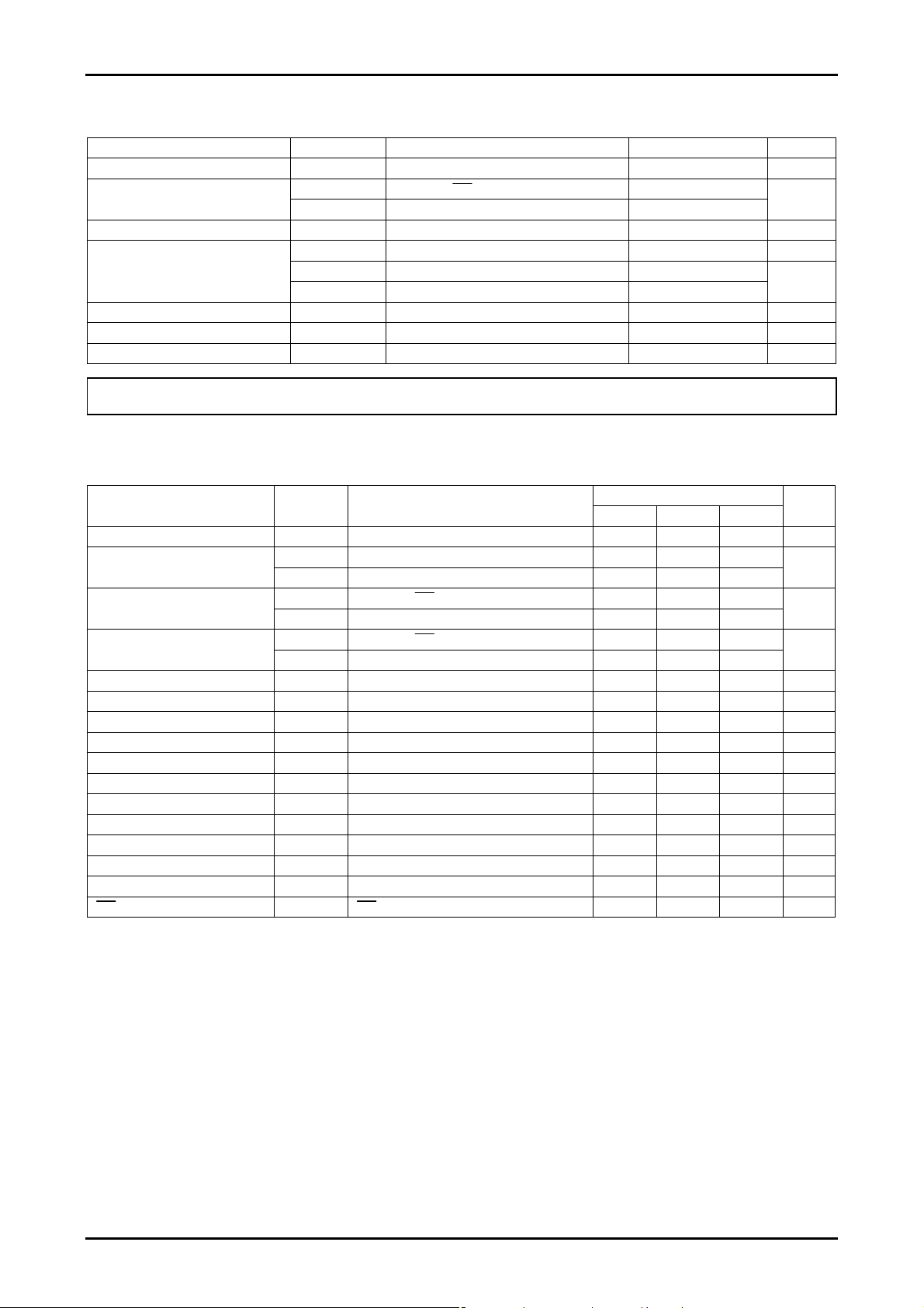
Absolute Maximum Ratings at Ta = 25°C, VSS = 0V
Parameter Symbol Conditions Ratings Unit
Maximum supply voltage VDD max VDD
Input voltage
Output voltage V
Output current
Allowable power dissipation Pd max Ta=85°C
Operating temperature Topr
Storage temperature Tstg
VIN1 CE, CL, DI,
VIN2 OSCI, VDD1, VDD2
S1 to S53, COM1 to COM4, P1 to P4
OUT
I
1 S1 to S52
OUT
I
2 COM1 to COM4, S53
OUT
I
3 P1 to P4
OUT
INH
Stresses exceeding Maximum Ratings may damage the device. Maximum Ratings are stress ratings only. Functional operation above the Recommended Operating
Conditions is not implied. Extended exposure to stresses above the Recommended Operating Conditions may affect device reliability.
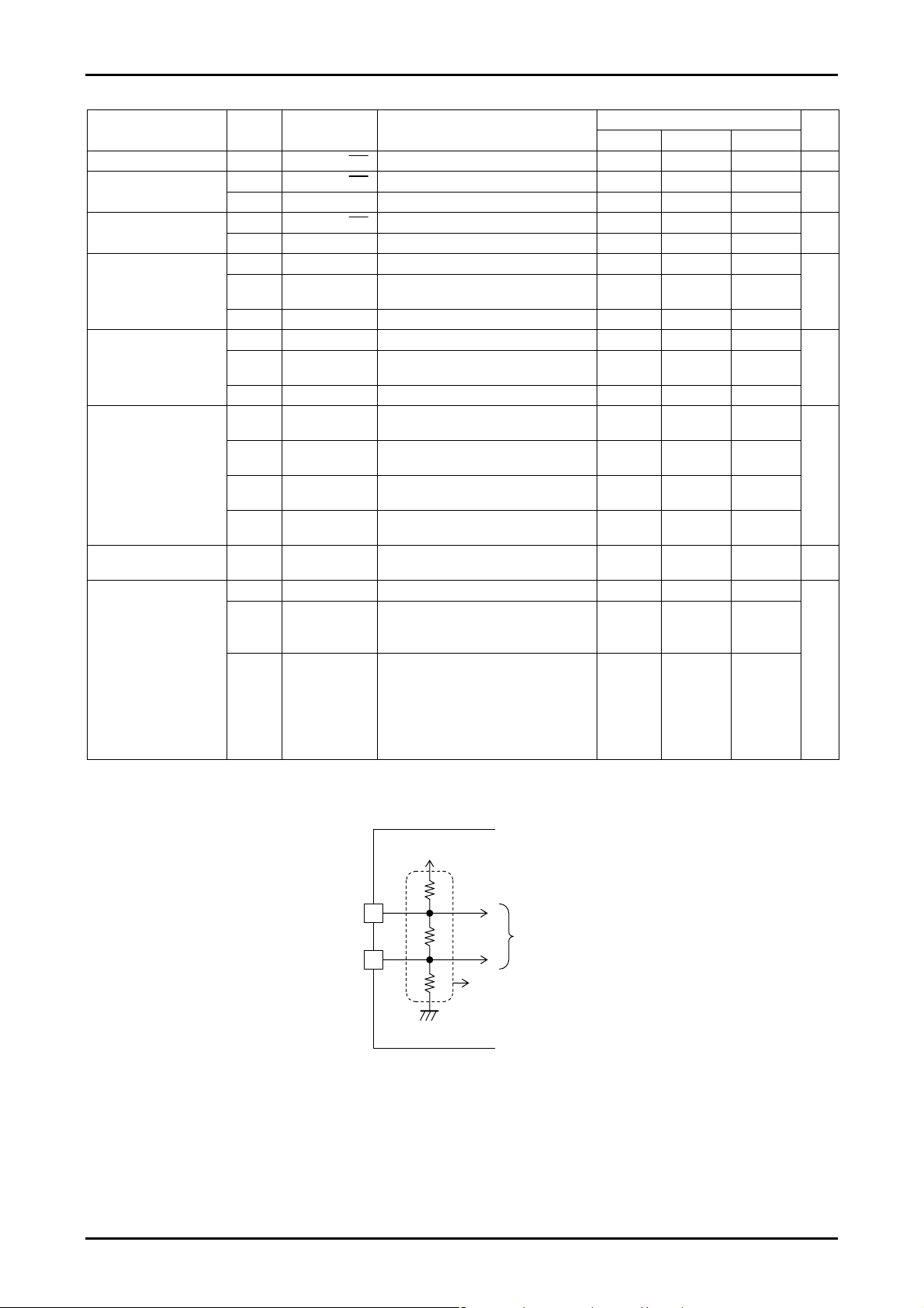
Allowable Operating Ranges at Ta = -40 to +85°C, VSS = 0V
Parameter Symbol Conditions
Supply voltage VDD VDD
Input voltage
Input high-level voltage
Input low-level voltage
External clock operating frequency fCK
External clock duty cycle DCK
Data setup time tds CL, DI [Figure 2][Figure 3]
Data hold time tdh CL, DI [Figure 2][Figure 3]
CE wait time tcp CE, CL [Figure 2][Figure 3]
CE setup time tcs CE, CL [Figure 2][Figure 3]
CE hold time tch CE, CL [Figure 2][Figure 3]
High-level clock pulse width
Low-level clock pulse width
Rise time tr CE, CL, DI [Figure 2][Figure 3]
Fall time tf CE, CL, DI [Figure 2][Figure 3]
switching time tc
INH
VDD1 VDD1
VDD2 VDD2
VIH1 CE, CL, DI,
VIH2 OSCI: External clock operating mode
VIL1 CE, CL, DI,
VIL2
tφH CL [Figure 2][Figure 3]
tφL CL [Figure 2][Figure 3]
OSCI: External clock operating mode
OSCI: External clock operating mode
OSCI: External clock operating mode
, CE [Figure 5][Figure 6]
INH
INH
INH
[Figure 4]
[Figure 4]
min typ max
4.5 6.0 V
0.4V
DD
0.4V
DD
0 0.2V
0 0.2V
10 300 600 kHz
30 50 70 %
160 ns
160 ns
160 ns
160 ns
160 ns
160 ns
160 ns
10 μs
-0.3 to +6.5 V
-0.3 to +6.5
-0.3 to VDD+0.3
-0.3 to VDD+0.3 V
300 μA
200 mW
-40 to +85 °C
-55 to +125 °C
Ratings
2/3VDD V
1/3VDD V
6.0
V
160 ns
160 ns
V
3
mA
5
DD
DD
DD
DD
DD
Unit
V
V
V
No.A1462-2/22
LC75829PE, 75829PW
SS
Electrical Characteristics for the Allowable Operating Ranges
Parameter Symbol Pin Conditions
Hysteresis VH CE, CL, DI,
Input high-level current
Input low-level current
Output high-level voltage
Output low-level voltage
Output middle-level
voltage *1
Oscillator frequency fosc Internal
Current drain
IIH1 CE, CL, DI,
IIH2 OSCI VI = VDD: External clock operating mode
IIL1 CE, CL, DI,
IIL2 OSCI VI = 0V: External clock operating mode
VOH1 S1 to S53 IO = -20μA
VOH2 COM1
to COM4
VOH3 P1 to P4 IO = -1mA
VOL1 S1 to S53 IO = 20μA
VOL2 COM1
to COM4
VOL3 P1 to P4 IO =1mA
V
1 S1 to S53 1/3 bias IO = ±20μA 2/3VDD
MID
V
2 S1 to S53 1/3 bias IO = ±20μA 1/3VDD
MID
V
3 COM1
MID
V
MID
IDD1 VDD Power-saving mode
IDD2 VDD V
IDD3 VDD V
to COM4
4 COM1
to COM4
oscillator circuit
INH
VI = 6.0V
INH
VI = 0V
INH
IO = -100μA
IO = 100μA
1/3 bias IO = ±100μA 2/3VDD
1/3 bias IO = ±100μA 1/3VDD
Internal oscillator operating mode
= 6.0V
DD
Output open
Internal oscillator operating mode
= 6.0V
DD
Output open
External clock operating mode
f
= 300kHz
CK
VIH2 = 0.5V
VIL2 = 0.1VDD
DD
min typ max
VDD-0.9
VDD-0.9
VDD-0.9
Note: *1 Excluding the bias voltage generation divider resistors built in the VDD1 and VDD2. (See Figure 1.)
V
DD
VDD1
To the common and segment drivers
VDD2
Except these resistors.
V
[Figure 1]
Ratings
0.03VDD V
5.0
5.0
-5.0
-5.0
0.9
0.9
0.9
2/3V
-0.9
-0.9
-0.9
-0.9
240 300 360 kHz
100
800 1600
800 1600
1/3V
2/3V
1/3V
DD
+0.9
DD
+0.9
DD
+0.9
DD
+0.9
Unit
μA
μA
V
V
V
μA
No.A1462-3/22
LC75829PE, 75829PW
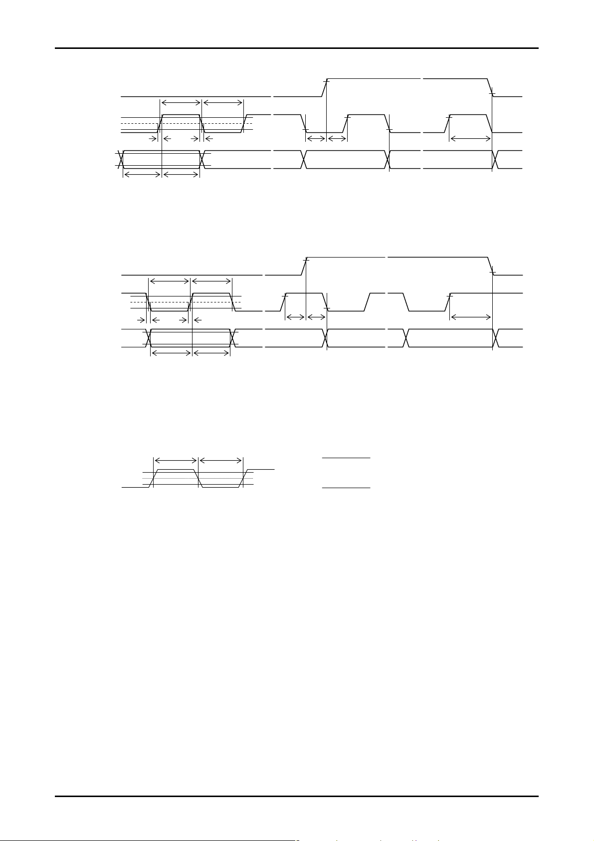
φ
φ
1. When CL is stopped at the low level
CE
L tφH
t
tr tf
tdh
t
≈ ≈ ≈ ≈
[Figure 2]
H tφL
VIH1
50%
VIL1
≈ ≈≈≈
VIH1
VIL1
[Figure 3]
tCKL tCKH
[Figure 4]
CL
DI
VIH1
50%
VIL1
VIH1
VIL1
tr tf
tds
tdh
2. When CL is stopped at the high level
CE
CL
DI
tds
3. OSCI pin clock timing in external clock operating mode
OSCI
VIH2
50%
VIL2
VIH1
VIH1
fCK=
DCK=
1
tCKH+ tCKL
tCKH
tCKH+ tCKL
≈ ≈≈≈
[kHz]
×100[%]
≈
VIL1
≈
≈ ≈
tch tcstcp
VIL1
tch tcstcp
No.A1462-4/22

LC75829PE, 75829PW
Package Dimensions Package Dimensions
unit : mm (typ) unit : mm (typ)
3159A [LC75829PE] 3190A [LC75829PW]
49
64
116
(1.0)
(2.7)
3.0max
0.1
0.8
17.2
14.0
3348
32
14.0
17.2
17
0.35
SANYO : QIP64E(14X14)
0.15
12.0
0.8
49
64
(1.25)
(1.5)
1.7max
0.1
10.0
3348
32
12.0
10.0
17
116
0.5
0.18
0.5
0.15
SANYO : SQFP64(10X10)
Pin Assignment
S51/COM4
S53/OSCI
S49
S50
COM3
COM2
COM1
S52
VDD
VDD1
VDD2
VSS
INH
CE
CL
DI
S48
S47
S46
S44
S45
LC75829PE
LC75829PW
S42
S43
S41
S40
S39
(QIP64E)
(SQFP64)
S38
S37
S36
S35
S34
3348
32 49
S32
S31
S30
S29
S28
S27
S26
S25
S24
S23
S22
S21
S20
S19
S18
S17
17 64
161
P1/S1
P2/S2
P4/S4
P3/S3
S5
S6
S7
S8
S9
S10
S11
S12
S13
S14
S15
S16 S33
Top view
No.A1462-5/22
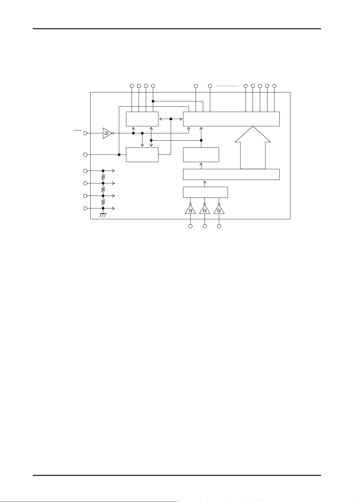
Block Diagram
INH
S53/OSCI
VDD
VDD1
VDD2
VSS
LC75829PE, 75829PW
COM3
COM2
COM1
COMMON
DRIVER
CLOCK
GENERATOR
COM4/S51
CONTROL
REGISTER
CCB INTERFACE
DI
S4/P4
S52
S50
SEGMENT DRIVER & LATCH
SHIFT REGISTER
CL
CE
S5
S2/P2
S3/P3
S1/P1
No.A1462-6/22
LC75829PE, 75829PW
Pin Functions
Symbol Pin No. Function Active I/O
S1/P1 to S4/P4
S5 to S50
S52
1 to 4
5 to 50
55
Segment outputs for displaying the display data transferred by serial data input.
The S1/P1 to S4/P4 pins can be used as general-purpose output ports under serial
data control.
Handling
when
unused
- O OPEN
COM1 to COM3
COM4/S51
S53/OSCI 60
CE 62 H I
CL 63
DI 64
INH
VDD1 57
VDD2 58
VDD 56
VSS 59
54 to 52
51
61
Common driver outputs
The frame frequency is fo[Hz].
The COM4/S51 pin can be used as a segment output in 1/3 duty.
Segment output. This pin can also be used as the external clock input pin when the
external clock operating mode is selected by control data.
Serial data transfer inputs. Must be connected to the controller.
CE: Chip enable
CL: Synchronization clock
DI: Transfer data
Display off control input
•
= low (VSS) ...Display forced off
INH
S1/P1 to S4/P4 = low (VSS)
(These pins are forcibly set to the general-purpose output port
function and held at the VSS level.)
S9 to S50, S52=low (VSS)
COM1 to COM3=low (VSS)
COM4/S51=low (VSS)
S53/OSCI=low (VSS)
(This pin is forcibly set to the segment output port function and
held at the VSS level.)
Stops the internal oscillator.
Inhibits external clock input.
•
= high (VDD)...Display on
INH
Enables the internal oscillator circuit.
(Internal oscillator operating mode)
Enables external clock input.
(External clock operating mode)
However, serial data transfer is possible when the display is forced off.
Used to apply the LCD drive 2/3 bias voltage externally.
Used to apply the LCD drive 1/3 bias voltage externally.
Power supply pin. A power voltage of 4.5 to 6.0V must be applied to this pin.
Ground pin. Must be connected to ground.
- O OPEN
- I/O OPEN
I GND
- I
L I GND
- I OPEN
- I OPEN
- - -
- - -
No.A1462-7/22

Serial Data Input
1. 1/4 duty
(1) When CL is stopped at the low level
CE
CL
0 0 0 01 0 0
D53 00 0 0 01 0 0
D105
D153
D2 D10 1
D54
D106
Display data
D154
B3 B2 A1 A0 A3 A2
B1 B0
CCB address
8 bits
0 1
B3 B2 A1 A0 A3 A2
B1 B0
CCB address
8 bits
0 1
B1 B0
B3 B2 A1 A0 A3 A2
CCB address
8 bits
0 1
B3 B2 A1 A0 A3 A2
B1 B0
CCB address
8 bits
Note: DD is the direction data.
Display data
Display data
48 bits
LC75829PE, 75829PW
D50
52 bits
D99
52 bits
D101 D102
D100
D152 D151
Display data
56 bits
D51
D203
D104 D103
D204
000
D208 D207 D206 D205 D202 D201 D200 D199
PS10
PS11
000001000 0 0 0 0 0 0000
000000010 0 0 0 0 00000000
Fixed data
22 bits
000001010 0 0 0 0
P2
Control data
18 bits
Fixed data
18 bits
Fixed data
P1P0DI
EXF
0 0 0 0 01 0 0
0 0 0 0 01 0 0
14 bits
FC0 FC1 FC2 D52 D47 D48 D49
SCOC DN DT
0
0
BU
00
DD
2 bits
DD
2 bits
DD
2 bits
DD
2 bits
No.A1462-8/22

LC75829PE, 75829PW
(2) When CL is stopped at the high level
CE
CL
DI
B1 B0
CCB address
B3 B2 A1 A0 A3 A2
8 bits
1 0 0
D2D1 0 0 0 0 1 0
D48 D47
Display data
52 bits
D50 D49 D52 D51
000 P1P0
PS10
PS11
EXF
Control data
18 bits
B1 B0
B3 B2 A1 A0 A3 A2
CCB address
8 bits
0 0 0 0 1 0
1 0 0 0000010
D54 D53
D100
D99
Display data
52 bits
D104 D103 D102 D101
Fixed data
18 bits
B1 B0
B3 B2 A1 A0 A3 A2
CCB address
8 bits
0 0 0 0 1 0
1 0 0 000000100 0 0 0 0 0
Display data
48 bits
D152 D106 D105 D151
00000 0 0 0
Fixed data
22 bits
B1 B0
B3 B2 A1 A0 A3 A2
CCB address
8 bits
0 0 0 0 1 0
1 0 0 000001100 0 0 0 0 0
Display data
56 bits
D204 D154 D153 D203
D208 D207 D206 D205 D202 D201 D200 D199
Fixed data
Note: DD is the direction data.
• CCB address .......... “41H”
• D1 to D208 ............ Display data
• PS10, PS11 ............ General-purpose output port (P1) function setting control data
• EXF ....................... External clock operating frequency setting control data
• P0 to P2 ................. Segment output port/general-purpose output port switching control data
• DT ......................... 1/4-duty 1/3-bias drive or 1/3-duty 1/3-bias drive switching control data
• DN ......................... S52 pin and S53/OSCI pin state setting control data
• FC0 to FC2 ............ Common/segment output waveform frame frequency control data
• OC ......................... Internal oscillator operating mode/external clock operating mode switching control data
• SC .......................... Segment on/off control data
• BU ......................... Normal mode/power-saving mode control data
FC0 SC
DTP2DN BU
00 0 0 0 0 00000
14 bits
OC FC1 FC2
0
0
0
00
DD
2 bits
DD
2 bits
DD
2 bits
DD
2 bits
No.A1462-9/22

2. 1/3 duty
(1) When CL is stopped at the low level
CE
CL
0 0 0
B1 B0
CCB address
B3 B2 A1 A0 A3 A2
8 bits
1 0 0
D2 D1 0 1
LC75829PE, 75829PW
D50
Display data
54 bits
D51
D53
D54
0
0
PS10
PS11
EXF
P1P0DI
P2
Control data
16 bits
FC0 FC1 FC2 D52 D47 D48 D49
SCOC DN DT
BU
00
DD
2 bits
0 1
B3 B2 A1 A0 A3 A2
B1 B0
CCB address
8 bits
0 1
B1 B0
B3 B2 A1 A0 A3 A2
CCB address
8 bits
Note: DD is the direction data.
D55 00 0 0 01 0 0
D109
D56
D110
Display data
54 bits
Display data
51 bits
D156 D155
D157 D158 D159
D106 D105
D1070D108 D103 D104 D101 D102
0
000001000 0 0 0 0 0 0
Fixed data
16 bits
000000010 0 0 0 0 0000
Fixed data
19 bits
0 0 0 0 01 0 0
DD
2 bits
0
DD
2 bits
No.A1462-10/22

(2) When CL is stopped at the high level
CE
CL
DI
B1 B0
B3 B2 A1 A0 A3 A2
CCB address
8 bits
1 0 0
D2 D10 0 0 0 1
LC75829PE, 75829PW
D50 D49 D52 D51
Display data
54 bits
D53D48 D47
0
D54
0P1P0
PS10
PS11
EXF
FC0
DT P2DN BU
Control data
16 bits
FC1 FC2
OC
SC
00
DD
2 bits
B1 B0
B3 B2 A1 A0 A3 A2
CCB address
8 bits
0 0 0 0 1
1 0 0 0
D56 D55
D101
Display data
54 bits
D107D102
D108
D106 D105 D104 D103
00010
0 0 0 0 0 0 00000
Fixed data
16 bits
0
0 0 0 0 1 0
B1 B0
B3 B2 A1 A0 A3 A2
CCB address
8 bits
1 0 0 00000010 0 0 0 0 0 0
Display data
D156 D110 D109 D155
D157 D158 D159
51 bits
0
0000
Fixed data
19 bits
0
Note: DD is the direction data.
• CCB address .......... “41H”
• D1 to D159 ............ Display data
• PS10, PS11 ............ General-purpose output port (P1) function setting control data
• EXF ....................... External clock operating frequency setting control data
• P0 to P2 ................. Segment output port/general-purpose output port switching control data
• DT ......................... 1/4-duty 1/3-bias drive or 1/3-duty 1/3-bias drive switching control data
• DN ......................... S52 pin and S53/OSCI pin state setting control data
• FC0 to FC2 ............ Common/segment output waveform frame frequency control data
• OC ......................... Internal oscillator operating mode/external clock operating mode switching control data
• SC .......................... Segment on/off control data
• BU ......................... Normal mode/power-saving mode control data
DD
2 bits
DD
2 bits
No.A1462-11/22

LC75829PE, 75829PW
Serial Data Transfer Example
1. 1/4 duty
• When 153 or more segments are used
All 288 bits of serial data must be sent.
1 0 0 0 0 0 1 0
B0 B1 B2 B3 A0 A1 A2 A3
D2 D1
D47
D48 D49 D50 D51
0000
D52
1 0 0 0 0 0 1 0
B0 B1 B2 B3 A0 A1 A2 A3
1 0 0 0 0 0 1 0
B0 B1 B2 B3 A0 A1 A2 A3
1 0 0 0 0 0 1 0
B0 B1 B2 B3 A0 A1 A2 A3
D53
D54 D99 D100
D105
D106
D153
D154 D199 D204
D101 D102
D151 D152
0000
00000000000 0 0 0 0 0 000
D103 D104
00000000000 0 0 0 0 0 00 01
• When fewer than 153 segments are used
Either 72, 144, or 216 bits of serial data must be sent, depending on the number of segments to be used.
However, the serial data shown below (the D1 to D52 display data and the control data) must always be sent.
1 0 0 0 0 0 1 0
B0 B1 B2 B3 A0 A1 A2 A3
D2 D1
D47
D48 D49 D50 D51
0000
D52
2. 1/3 duty
• When 109 or more segments are used
All 216 bits of serial data must be sent.
1 0 0 0 0 0 1 0
B0 B1 B2 B3 A0 A1 A2 A3
D2 D1
D47
D48 D49 D50 D51 D53 D54
D52
1 0 0 0 0 0 1 0
B0 B1 B2 B3 A0 A1 A2 A3
D55
D56
D101 D102 D103 D104
D105 D106
D107 D108
1 0 0 0 0 0 1 0
B0 B1 B2 B3 A0 A1 A2 A3
D109
D110
D155 D156
D157 D158 D159
00000000000 0 0 0 0 0 00 01
0
• When fewer than 109 segments are used
Either 72, or 144 bits of serial data must be sent, depending on the number of segments to be used.
However, the serial data shown below (the D1 to D54 display data and the control data) must always be sent.
72 bits 8 bits
PS11
PS10
0 0 0 0 0 0 0 0 0 0 0 0 0 0 11
D208D207D206D205D203D202D201D200
72 bits8 bits
PS10
72 bits 8 bits
00
PS10
000000000 0 0 0 0 0 000
P0 P1 P2 DT DN
PS11
EXF
P0 P1 P2 DT DN
PS11
P0 P1 P2 DT DN
FC0 EXF
FC0
FC0 EXF
FC1 FC2
FC1 FC2
FC1 FC2
OC SC BU 0 0
1
OC SC BU 0 0
OC SC BU 0 0
1
1 0 0 0 0 0 1 0
B0 B1 B2 B3 A0 A1 A2 A3
72 bits8 bits
D47
D2 D1
D48 D49 D50 D51 D53 D54
D52
00
PS10
PS11
P0 P1 P2 DT DN
FC0 EXF
FC1 FC2
OC SC BU 0 0
No.A1462-12/22

LC75829PE, 75829PW
Control Data Functions
(1) PS10 and PS11 … General-purpose output port (P1) function setting control data
These control data bits set the clock output or general-purpose output function (High or low level output) of the P1
output pin.
PS10 PS11 General-purpose output port (P1) function
0 0 General-purpose output function (High or low level output)
1 0 Clock output function (Clock frequency : fosc/2, fCK/2)
0 1 Clock output function (Clock frequency : fosc/8, fCK/8)
Note: When is setting (PS10, PS11)=(1,1), the P1 output pin selects the general-purpose output function
(High or low level output).
(2) EXF … External clock operating frequency setting control data
This control data sets the operating frequency of the external clock which input into the OSCI pin, when the external
clock operating mode (OC=”1”) is set. However, this data is effective only when external clock operating mode
(OC= "1") is set.
EXF External clock operating frequency fCK[kHz]
0 fCK1=300[kHz]typ
1 fCK2=38[kHz]typ
(3) P0 to P2 … Segment output port/general-purpose output port switching control data
These control data bits switch the segment output port/general-purpose output port functions of the S1/P1 to S4/P4
output pins.
Control data Output pin state
P0 P1 P2 S1/P1 S2/P2 S3/P3 S4/P4
0 0 0 S1 S2 S3 S4
0 0 1 P1 S2 S3 S4
0 1 0 P1 P2 S3 S4
0 1 1 P1 P2 P3 S4
1 0 0 P1 P2 P3 P4
Note: When are setting (P0,P1,P2)=(1,0,1), (1,1,0), and (1,1,1), the all P1/S1 to P4/S4 output pins selects the
segment output port.
The table below lists the correspondence between the display data and the output pins when these pins are selected
to be general-purpose output ports.
Output pin
S1/P1 D1 D1
S2/P2 D5 D4
S3/P3 D9 D7
S4/P4 D13 D10
Correspondence display data
1/4 duty 1/3 duty
For example, if the circuit is operated in 1/4 duty and the S4/P4 output pin is selected to be a general-purpose output
port, the S4/P4 output pin will output a high level (VDD) when the display data D13 is 1, and will output a low level
(VSS) when D13 is 0.
(4) DT … 1/4-duty 1/3-bias drive or 1/3-duty 1/3-bias drive switching control data
This control data bit selects either 1/4-duty 1/3-bias drive or 1/3-duty 1/3-bias drive.
DT Drive scheme The COM4/S51 pin state
0 1/4-duty 1/3-bias drive COM4
1 1/3-duty 1/3-bias drive S51
Note: Sn (n=1 to 4): Segment output ports
Pn (n=1 to 4): General-purpose output ports
Note: COM4: Common output
S51 : Segment output
No.A1462-13/22
LC75829PE, 75829PW
(5) DN … S52 pin and S53/OSCI pin state setting control dat a
This control data bit sets state of the S52 pin and the S53/O SC I pin.
DN
0 Up to 200 segments Up to 153 segments “L” (VSS) “L” (VSS)/OSCI
1 Up to 208 segments Up to 159 segments S52 S53/OSCI
Note: “L” (VSS) : Low (VSS) level output
S52 : Segment output
“L” (VSS)/OSCI : Low (VSS) level output in internal oscillator operating mode (OC=0)
: External clock input in external clock operating mode (OC=1)
S53/OSCI : Segment output in internal oscillator operating mode (OC=0)
(6) FC0 to FC2 … Common/segment output waveform fram frequency control data
These control data bits set the frame frequency of the common and segment output waveforms.
Control data Frame frequency fo[Hz]
FC0 FC1 FC2
0 0 0 fosc/6144 fCK1/6144 fCK2/768
0 0 1 fosc/4608 fCK1/4608 fCK2/576
0 1 0 fosc/3072 fCK1/3072 fCK2/384
0 1 1 fosc/2304 fCK1/2304 fCK2/288
1 0 0 fosc/1536 fCK1/1536 fCK2/192
1 0 1 fosc/1152 fCK1/1152 fCK2/144
1 1 0 fosc/768 fCK1/768 fCK2/96
Note: When is setting (FC0,FC1,FC2)=(1,1,1), the frame frequency is same as frame frequency at the time of the
(FC0,FC1,FC2)=(0,1,0) setting (fosc/3072, fCK1/3072, fCK2/384).
(7) OC … Internal oscillator operating mode/external clock operating mode switching control data
This control data bit selects either the internal oscillator operating mode or external clock operating mode.
OC Fundamental clock operating mode
0 Internal oscillator operating mode S53
1 External clock operating mode OSCI
Note: S53: Segment output
OSCI: External clock input
(8) SC … Segment on/off control data
This control data bit controls the on/off state of the segments.
SC Display state
0 On
1 Off
Note that when the segments are turned off by setting SC to 1, the segments are turned off by outputting segment off
waveforms from the segment output pins.
(9) BU … Normal mode/power-saving mode control data
This control data bit selects either normal mode or power-saving mode.
BU Mode
0 Normal mode
Power saving mode
In this mode, the internal oscillator circuit stops oscillation (the S53/OSCI pin is configured for segment
output) if the IC is in the internal oscillator operating mode (OC=0) and the IC stops receiving external
1
clock signals (the S53/OSCI pin is configured for external clock input) if the IC is in the external clock
operating mode (OC=1). The common and segment output pins go to the VSS level. Howe ver, the S1/P1
to S4/P4 output pins can be used as general-purpose output ports under the control of the data bits P0 to
P2. (The general-purpose output port P1 can not be used as clock output).
Number of display segments Pin state
1/4 duty 1/3 duty S52 S53/OSCI
External clock input in external clock operating mode (OC=1)
Internal oscillator operating mode
(The control data OC is 0,
fosc=300[kHz]typ)
External clock operating mode
(The control data OC is 1
and EXF is 0, fCK1=300[kHz]typ)
I/O pin (S53/OSCI) state
External clock operating mode
(The control data OC is 1
and EXF is 1, fCK2=38[kHz]typ)
No.A1462-14/22

LC75829PE, 75829PW
Display Data and Output Pin Correspondence (1/4 Duty)
Output pin CO M1 CO M2 COM3 COM4 Output pin COM1 COM2 COM3 COM4
S1/P1 D1 D2 D3 D4 S27 D105 D106 D107 D108
S2/P2 D5 D6 D7 D8 S28 D109 D110 D111 D112
S3/P3 D9 D10 D11 D12 S29 D113 D114 D115 D116
S4/P4 D13 D14 D15 D16 S30 D117 D118 D119 D120
S5 D17 D18 D19 D20 S31 D121 D122 D123 D124
S6 D21 D22 D23 D24 S32 D125 D126 D127 D128
S7 D25 D26 D27 D28 S33 D129 D130 D131 D132
S8 D29 D30 D31 D32 S34 D133 D134 D135 D136
S9 D33 D34 D35 D36 S35 D137 D138 D139 D140
S10 D37 D38 D39 D40 S36 D141 D142 D143 D144
S11 D41 D42 D43 D44 S37 D145 D146 D147 D148
S12 D45 D46 D47 D48 S38 D149 D150 D151 D152
S13 D49 D50 D51 D52 S39 D153 D154 D155 D156
S14 D53 D54 D55 D56 S40 D157 D158 D159 D160
S15 D57 D58 D59 D60 S41 D161 D162 D163 D164
S16 D61 D62 D63 D64 S42 D165 D166 D167 D168
S17 D65 D66 D67 D68 S43 D169 D170 D171 D172
S18 D69 D70 D71 D72 S44 D173 D174 D175 D176
S19 D73 D74 D75 D76 S45 D177 D178 D179 D180
S20 D77 D78 D79 D80 S46 D181 D182 D183 D184
S21 D81 D82 D83 D84 S47 D185 D186 D187 D188
S22 D85 D86 D87 D88 S48 D189 D190 D191 D192
S23 D89 D90 D91 D92 S49 D193 D194 D195 D196
S24 D93 D94 D95 D96 S50 D197 D198 D199 D200
S25 D97 D98 D99 D100 S52 D201 D202 D203 D204
S26 D101 D102 D103 D104 S53/OSCI D205 D206 D207 D208
Note: This table assumes that pins S1/P1 to S4/P4 and S53/OSCI are configured for segment output.
For example, the table below lists the output states for the S21 output pin.
Display data
D81 D82 D83 D84
0 0 0 0 The LCD segments corresponding to COM1, COM2, COM3, and COM4 are off.
0 0 0 1 The LCD segment corresponding to COM4 is on.
0 0 1 0 The LCD segment corresponding to COM3 is on.
0 0 1 1 The LCD segments corresponding to COM3 and COM4 are on.
0 1 0 0 The LCD segment corresponding to COM2 is on.
0 1 0 1 The LCD segments corresponding to COM2 and COM4 are on.
0 1 1 0 The LCD segments corresponding to COM2 and COM3 are on.
0 1 1 1 The LCD segments corresponding to COM2, COM3, and COM4 are on.
1 0 0 0 The LCD segment corresponding to COM1 is on.
1 0 0 1 The LCD segments corresponding to COM1 and COM4 are on.
1 0 1 0 The LCD segments corresponding to COM1 and COM3 are on.
1 0 1 1 The LCD segments corresponding to COM1, COM3, and COM4 are on.
1 1 0 0 The LCD segments corresponding to COM1 and COM2 are on.
1 1 0 1 The LCD segments corresponding to COM1, COM2, and COM4 are on.
1 1 1 0 The LCD segments corresponding to COM1, COM2, and COM3 are on.
1 1 1 1 The LCD segments corresponding to COM1, COM2, COM3, and COM4 are on.
Output pin (S21) state
No.A1462-15/22

LC75829PE, 75829PW
Display Data and Output Pin Correspondence (1/3 Duty)
Output pin COM1 COM2 COM3 Output pin COM1 COM2 COM3
S1/P1 D1 D2 D3 S28 D82 D83 D84
S2/P2 D4 D5 D6 S29 D85 D86 D87
S3/P3 D7 D8 D9 S30 D88 D89 D90
S4/P4 D10 D11 D12 S31 D91 D92 D93
S5 D13 D14 D15 S32 D94 D95 D96
S6 D16 D17 D18 S33 D97 D98 D99
S7 D19 D20 D21 S34 D100 D101 D102
S8 D22 D23 D24 S35 D103 D104 D105
S9 D25 D26 D27 S36 D106 D107 D108
S10 D28 D29 D30 S37 D109 D110 D111
S11 D31 D32 D33 S38 D112 D113 D114
S12 D34 D35 D36 S39 D115 D116 D117
S13 D37 D38 D39 S40 D118 D119 D120
S14 D40 D41 D42 S41 D121 D122 D123
S15 D43 D44 D45 S42 D124 D125 D126
S16 D46 D47 D48 S43 D127 D128 D129
S17 D49 D50 D51 S44 D130 D131 D132
S18 D52 D53 D54 S45 D133 D134 D135
S19 D55 D56 D57 S46 D136 D137 D138
S20 D58 D59 D60 S47 D139 D140 D141
S21 D61 D62 D63 S48 D142 D143 D144
S22 D64 D65 D66 S49 D145 D146 D147
S23 D67 D68 D69 S50 D148 D149 D150
S24 D70 D71 D72 S51/COM4 D151 D152 D153
S25 D73 D74 D75
S26 D76 D77 D78 S53/OSCI D157 D158 D159
S27 D79 D80 D81
Note: This table assumes that pins S1/P1 to S4/P4, S51/COM4, and S53/OSCI are configured for segment output.
For example, the table below lists the output states for the S21 output pin.
Display data
D61 D62 D63
0 0 0 The LCD segments corresponding to COM1, COM2, and COM3 are off.
0 0 1 The LCD segment corresponding to COM3 is on.
0 1 0 The LCD segment corresponding to COM2 is on.
0 1 1 The LCD segments corresponding to COM2 and COM3 are on.
1 0 0 The LCD segment corresponding to COM1 is on.
1 0 1 The LCD segments corresponding to COM1 and COM3 are on.
1 1 0 The LCD segments corresponding to COM1 and COM2 are on.
1 1 1 The LCD segments corresponding to COM1, COM2, and COM3 are on.
S52 D154 D155 D156
Output pin (S21) state
No.A1462-16/22

LC75829PE, 75829PW
Output Waveforms (1/4-Duty 1/3-Bias Drive Scheme)
COM1
COM2
COM3
COM4
LCD driver output when all LCD segments
corresponding to COM1, COM2, COM3, and
COM4 are off.
LCD driver output when only LCD segments
corresponding to COM1 are on.
LCD driver output when only LCD segments
corresponding to COM2 are on.
LCD driver output when LCD segments
corresponding to COM1 and COM2 are on.
LCD driver output when only LCD segments
corresponding to COM3 are on.
LCD driver output when LCD segments
corresponding to COM1 and COM3 are on.
LCD driver output when LCD segments
corresponding to COM2 and COM3 are on.
LCD driver output when LCD segments
corresponding to COM1, COM2, and COM3
are on.
LCD driver output when only LCD segments
corresponding to COM4 are on.
LCD driver output when LCD segments
corresponding to COM2 and COM4 are on.
LCD driver output when all LCD segments
corresponding to COM1, COM2, COM3, and
COM4 are on.
Control data Frame frequency fo[Hz]
Internal oscillator operating mode
FC0 FC1 FC2
0 0 0 fosc/6144 fCK1/6144 fCK2/768
0 0 1 fosc/4608 fCK1/4608 fCK2/576
0 1 0 fosc/3072 fCK1/3072 fCK2/384
0 1 1 fosc/2304 fCK1/2304 fCK2/288
1 0 0 fosc/1536 fCK1/1536 fCK2/192
1 0 1 fosc/1152 fCK1/1152 fCK2/144
1 1 0 fosc/768 fCK1/768 fCK2/96
(The control data OC is 0,
fosc=300[kHz]typ)
Note: When is setting (FC0,FC1,FC2)=(1,1,1), the frame frequency is same as frame frequency at the time of the
(FC0,FC1,FC2)=(0,1,0) setting (fosc/3072, fCK1/3072, fCK2/384).
fo[Hz]
External clock operating mode
(The control data OC is 1
and EXF is 0, fCK1=300[kHz]typ)
VDD
VDD1
VDD2
0V
VDD
VDD1
VDD2
0V
VDD
VDD1
VDD2
0V
VDD
VDD1
VDD2
0V
VDD
VDD1
VDD2
0V
VDD
VDD1
VDD2
0V
VDD
VDD1
VDD2
0V
VDD
VDD1
VDD2
0V
VDD
VDD1
VDD2
0V
VDD
VDD1
VDD2
0V
VDD
VDD1
VDD2
0V
VDD
VDD1
VDD2
0V
VDD
VDD1
VDD2
0V
VDD
VDD1
VDD2
0V
VDD
VDD1
VDD2
0V
External clock operating mode
(The control data OC is 1
and EXF is 1, fCK2=38[kHz]typ)
No.A1462-17/22

LC75829PE, 75829PW
[Hz]
Output waveforms (1/3-Duty 1/3-Bias Drive Scheme)
COM1
COM2
COM3
LCD driver output when all LCD segments
corresponding to COM1, COM2, and COM3
are off.
LCD driver output when only LCD segments
corresponding to COM1 are on.
LCD driver output when only LCD segments
corresponding to COM2 are on.
LCD driver output when LCD segments
corresponding to COM1 and COM2 are on.
LCD driver output when only LCD segments
corresponding to COM3 are on.
LCD driver output when LCD segments
corresponding to COM1 and COM3 are on.
LCD driver output when LCD segments
corresponding to COM2 and COM3 are on.
LCD driver output when all LCD segments
corresponding to COM1, COM2, and COM3
are on.
Control data Frame frequency fo[Hz]
Internal oscillator operating mode
FC0 FC1 FC2
0 0 0 fosc/6144 fCK1/6144 fCK2/768
0 0 1 fosc/4608 fCK1/4608 fCK2/576
0 1 0 fosc/3072 fCK1/3072 fCK2/384
0 1 1 fosc/2304 fCK1/2304 fCK2/288
1 0 0 fosc/1536 fCK1/1536 fCK2/192
1 0 1 fosc/1152 fCK1/1152 fCK2/144
1 1 0 fosc/768 fCK1/768 fCK2/96
Note: When is setting (FC0,FC1,FC2)=(1,1,1), the frame frequency is same as frame frequency at the time of the
(FC0,FC1,FC2)=(0,1,0) setting (fosc/3072, fCK1/3072, fCK2/384).
(The control data OC is 0,
fosc=300[kHz]typ)
fo
External clock operating mode
(The control data OC is 1
and EXF is 0, fCK1=300[kHz]typ)
V
VDD1
VDD2
0V
V
VDD1
VDD2
0V
V
VDD1
VDD2
0V
V
VDD1
VDD2
0V
V
VDD1
VDD2
0V
V
VDD1
VDD2
0V
V
VDD1
VDD2
0V
V
VDD1
VDD2
0V
V
VDD1
VDD2
0V
V
VDD1
VDD2
0V
V
VDD1
VDD2
0V
External clock operating mode
(The control data OC is 1
and EXF is 1, fCK2=38[kHz]typ)
DD
DD
DD
DD
DD
DD
DD
DD
DD
DD
DD
No.A1462-18/22

LC75829PE, 75829PW
Display Control and the
INH
Pin
Since the LSI internal data (1/4 duty : the display data D1 to D208 and the control data, 1/3 duty : the display data D1 to
D159 and the control data) is undefined when power is first applied, applications should set the INH
pin low at the same
time as power is applied to turn off the display (This sets the S1/P1 to S4/P4, S5 to S50, COM1 to COM3, COM4/S51,
S52, and S53/OSCI pins to the VSS level.) and during this period send serial data from the controller. The controller
should then set the INH
pin high after the data transfer has completed. This procedure prevents meaningless display at
power on.
(See Figure 5 and Figure 6.)
• 1/4 duty
t1
VDD
t2
Internal data
Internal data (D53 to D104)
INH
CE
D1 to D52,PS10,PS11,
EXF,P0 to P2,DT,DN,
FC0 to FC2,OC,SC,BU
Undefined
Undefined
Display data and control
data transferred
tc
VIL1
Defined
Defined
VIL1
Undefined
Undefined
Internal data (D105 to D152)
Undefined
Defined
Undefined
Internal data (D153 to D208)
Undefined
[Figure 5]
Defined
Undefined
Notes: t1>1ms
t2>0
tc…10μs min
• 1/3 duty
t1
VDD
t2
Internal data
Internal data (D55 to D108)
INH
CE
D1 to D54,PS10,PS11,
EXF,P0 to P2,DT,DN,
FC0 to FC2,OC,SC,BU
Undefined
Undefined
Display data and control
data transferred
tc
VIL1
Defined
Defined
VIL1
Undefined
Undefined
Internal data (D109 to D159)
Undefined
Defined
Undefined
[Figure 6]
Notes: t1>1ms
t2>0
tc…10μs min
No.A1462-19/22

LC75829PE, 75829PW
Notes on Controller Transfer of Display Data
When using the LC75829 in 1/4 duty, applications transfer the display data (D1 to D208) in four operations, and in 1/3
duty, they transfer the display data (D1 to D159) in three operations. In either case, applications should transfer all of
the display data within 30 ms to maintain the quality of displayed image.
S53/OSCI Pin Peripheral Circuit
(1) Internal oscillator operating mode (control data OC=0)
Connect the S53/OSCI pin to the LCD panel when the internal oscillator operating mode is selected.
(2) External clock operating mode (control data OC=1)
When the external clock operating mode is selected, insert a current protection resistor Rg (2.2 to 22kΩ) between
the S53/OSCI pin and external clock output pin (external oscillator). Determine the value of the resistance according
to the allowable current value at the external clock output pin. Also make sure that the waveform of the external
clock is not heavily distorted.
(3) Unused pin treatment
When the S53/OSCI pin is not to be used, select the internal oscillator operating mode (setting control
data OC to 0) to keep the pin open.
OSCI/S53
External oscillator
OSCI/S53
To LCD panel
OSCI/S53External clock output pin
Rg
Note: Allowable current value at external clock output pin >
OPEN
V
DD
Rg
No.A1462-20/22

LC75829PE, 75829PW
μ
μ
Sample Applications Circuit1
1/4 Duty, 1/3 Bias
(P1)
(P2)
(P3)
(P4)
+5V
C
C
V
DD
VDD1
VDD2
V
SS
C≥0.047
F
COM1
COM2
COM3
S51/COM4
P1/S1
P2/S2
P3/S3
P4/S4
S5
From the
controller
INH
CE
CL
DI
*2
*3
S50
S52
OSCI/S53
*2 The pins to be connected to the controller (CE, CL, DI, INH
) can handle 3.3V or 5V.
*3 Connect the S53/OSCI pin to the LCD panel in the internal oscillator operating mode and insert a current protection
resistor Rg (2.2 to 22kΩ) between the S53/OSCI pin and external clock output pin (external oscillator) in the
external clock operating mode (see “S53/OSCI Pin Peripheral Circuit”).
General-purpose
output ports
Used for functions
such as backlight
control
LCD panel (up to 208 segments)
Sample Application Circuit 2
1/3 Duty, 1/3 Bias
(P1)
(P2)
(P3)
(P4)
+5V
V
DD
VDD1
C
C
VDD2
V
SS
C≥0.047
F
COM1
COM2
COM3
P1/S1
P2/S2
P3/S3
P4/S4
S5
From the
controller
INH
CE
CL
DI
*2
*3
S50
COM4/S51
S52
OSCI/S53
*2 The pins to be connected to the controller (CE, CL, DI, INH
) can handle 3.3V or 5V.
*3 Connect the S53/OSCI pin to the LCD panel in the internal oscillator operating mode and insert a current protection
resistor Rg (2.2 to 22kΩ) between the S53/OSCI pin and external clock output pin (external oscillator) in the
external clock operating mode (see “S53/OSCI Pin Peripheral Circuit”).
General-purpose
output ports
Used for functions
such as backlight
control
LCD panel (up to 159 segments)
No.A1462-21/22

LC75829PE, 75829PW
ON Semiconductorand the ON logo are registered trademarks of Semiconductor Components Industries, LLC (SCILLC) . SCILLC owns the rights to a number
of patents, trademarks, copyrights, trade secrets, and other intellectual property. A listing of SCILLC’s product/patent coverage may be accessed at
www.onsemi.com/site/pdf/Patent-Marking.pdf. SCILLC reserves the right to make changes without further notice to any products herein. SCILLC makes no
warranty, representation or guaranteeregarding the suitabilityof its products for any particular purpose, nor does SCILLC assume any liability arising out of the
application or use of any product or circuit, and specifically disclaims any and all liability, including without limitation special, consequential or incidental
damages. “Typical” parameters which may be provided in SCILLC data sheets and/or specifications can and do vary in different applications and actual
performance may vary over time. All operating parameters, including “Typicals” must be validated for each customer application by customer’s technical
experts. SCILLC does not convey any license under its patent rights nor the rights of others. SCILLC products are not designed, intended, or authorizedfor use
as components in systems intended for surgical implant into the body, or other applications intended to support or sustain life, or for any other application in
which the failure of the SCILLC product could create a situation where personal injury or death may occur. Should Buyer purchase or use SCILLC products for
any such unintended or unauthorized application, Buyer shall indemnify and hold SCILLC and its officers, employees, subsidiaries, affiliates, and distributors
harmless against all claims, costs, damages, and expenses, and reasonable attorney fees arising out of, directly or indirectly, any claim of personal injury or
death associated with such unintended or unauthorized use, even if such claim alleges that SCILLC was negligent regarding the design or manufacture ofthe
part. SCILLC is an Equal Opportunity/Affirmative Action Employer. This literature is subject to all applicable copyright laws and is not for resale in any manner.
No.A1462-22/22
PS
 Loading...