

Page 1
查询NCV4949供应商
L4949, NCV4949
100 mA, 5.0 V, Low Dropout
Voltage Regulator with
Power-On Reset
The L4949 is a monolithic integrated 5.0 V voltage regulator with a
very low dropout and additional functions such as power–on reset and
input voltage sense.
It is designed for supplying the micro–computer controlled systems
especially in automotive applications.
• Operating DC Supply Voltage Range 5.0 V to 28 V
• Transient Supply Voltage Up to 40 V
• Extremely Low Quiescent Current in Standby Mode
• High Precision Standby Output Voltage 5.0 V ±1%
• Output Current Capability Up to 100 mA
• Very Low Dropout Voltage Less Than 0.4 V
• Reset Circuit Sensing The Output Voltage
• Programmable Reset Pulse Delay With External Capacitor
• Voltage Sense Comparator
• Thermal Shutdown and Short Circuit Protections
http://onsemi.com
MARKING
DIAGRAMS
PDIP–8
8
1
8
1
N SUFFIX
CASE 626
SO–8
D SUFFIX
CASE 751
8
L4949N
AWL
YYWW
1
8
L4949
ALYWD
1
Supply
Voltage (V
Sense
CC
Input
(S
A = Assembly Location
WL, L = Wafer Lot
YY, Y = Year
WW, W = Work Week
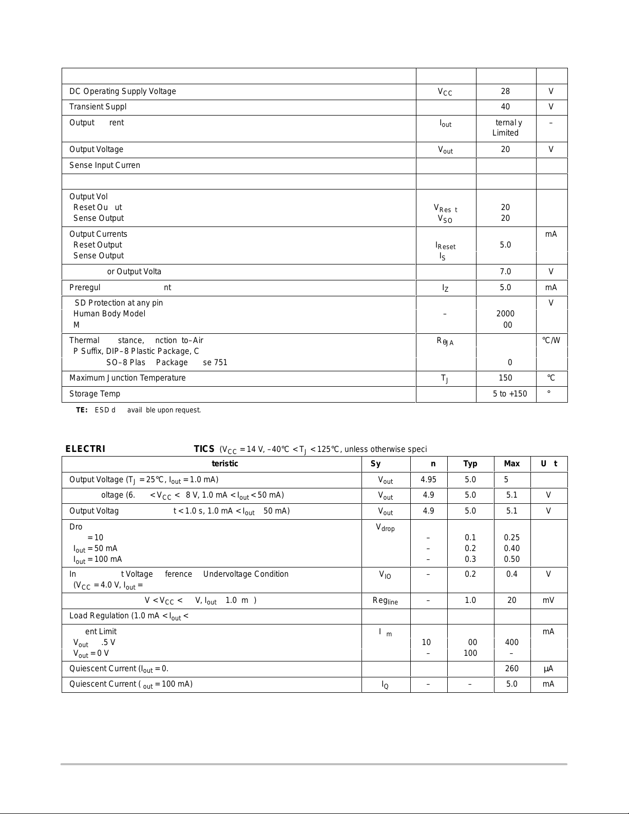
PIN CONNECTIONS
Representative Block Diagram
Output
2.0 µA
Reset
)
out
C
T
Reset
6
+
2.0 V
Sense
-
+
1.23 V
-
Sense
Output
)
(S
o
7
Voltage (V
V
38 4
Z
)
1
)
i
2
V
s
Preregulator
6.0 V
Regulator
1.23 V
ref
V
1
CC
S
2
i
V
3
Z
C
4
T
(Top View)
V
8
out
S
7
o
Reset
6
Gnd
5
ORDERING INFORMATION
See detailed ordering and shipping information in the package
dimensions section on page 8 of this data sheet.
Semiconductor Components Industries, LLC, 2002
April, 2002 – Rev. 4
5
Gnd
1 Publication Order Number:
L4949/D
Page 2
L4949, NCV4949
Á
Á
Á
Á
ÁÁÁ
ÁÁÁ
ÁÁÁ
ÁÁÁ
ÁÁÁ
ÁÁÁ
ÁÁÁ
ÁÁÁ
ÁÁÁ
ÁÁÁ
ÁÁÁ
ÁÁÁ
ÁÁÁ
ABSOLUTE MAXIMUM RATINGS (Absolute Maximum Ratings indicate limits beyond which damage to the device may occur.)
Rating Symbol Value Unit
DC Operating Supply Voltage
Transient Supply Voltage (t < 1.0 s)
Output Current
ББББББББББББББББББББББ
Output Voltage
Sense Input Current
Sense Input Voltage
Output Voltages
Reset Output
Sense Output
Output Currents
Reset Output
Sense Output
Preregulator Output Voltage
Preregulator Output Current
ESD Protection at any pin
Human Body Model
Machine Model
Thermal Resistance, Junction–to–Air
P Suffix, DIP–8 Plastic Package, Case 626
D Suffix, SO–8 Plastic Package, Case 751
Maximum Junction Temperature
Storage Temperature Range
NOTE: ESD data available upon request.
V
CC
V
CC TR
I
out
ÁÁÁ
V
out
I
SI
V
SI
V
Reset
V
SO
I
Reset
I
SO
V
Z
I
Z
–
–
R
θ
JA
T
J
T
stg
28
40
Internally
Limited
ÁÁ
20
±1.0
V
CC
20
20
5.0
5.0
7.0
5.0
2000
400
100
200
150
–65 to +150
V
V
–
Á
V
mA
–
V
mA
V
mA
V
°C/W
°C
°C
ELECTRICAL CHARACTERISTICS (V
= 14 V, –40°C < TJ < 125°C, unless otherwise specified.)
CC
Characteristic
Output Voltage (TJ = 25°C, I
Output Voltage (6.0 V < VCC < 28 V, 1.0 mA < I
Output Voltage (VCC = 35 V, t < 1.0 s, 1.0 mA < I
= 1.0 mA)
out
< 50 mA)
out
out
< 50 mA)
Dropout Voltage
I
= 10 mA
out
I
= 50 mA
out
I
= 100 mA
out
Input to Output Voltage Difference in Undervoltage Condition
(VCC = 4.0 V, I
Line Regulation (6.0 V < VCC < 28 V, I
Load Regulation (1.0 mA < I
= 35 mA)
out
< 100 mA)
out
= 1.0 mA)
out
Current Limit
V
= 4.5 V
out
V
= 0 V
out
Quiescent Current (I
Quiescent Current (I
= 0.3 mA, TJ < 100°C)
out
= 100 mA)
out
Symbol Min Typ Max Unit
V
V
V
V
Reg
Reg
I
out
out
out
drop
V
IO
I
Lim
QSE
I
Q
line
load
4.95
4.9
4.9
–
–
–
–
–
–
105
–
–
–
5.0
5.0
5.0
0.1
0.2
0.3
0.2
1.0
8.0
200
100
150
–
5.05
5.1
5.1
0.25
0.40
0.50
0.4
20
30
400
–
260
5.0
V
V
V
V
V
mV
mV
mA
µA
mA
http://onsemi.com
2
Page 3
L4949, NCV4949
ÁÁÁ
ÁÁÁ
ÁÁÁ
ÁÁÁ
ÁÁÁ
ÁÁÁ
ÁÁÁ
ÁÁÁ
ÁÁÁ
ÁÁÁ
ÁÁÁ
ÁÁÁ
ÁÁÁ
ÁÁÁ
ÁÁÁ
ELECTRICAL CHARACTERISTICS (continued) (V
= 14 V, –40°C < TJ < 125°C, unless otherwise specified.)
CC
Characteristic UnitMaxTypMinSymbol
RESET
Reset Threshold Voltage
Reset Threshold Hysteresis
@ TJ = 25°C
@ TJ = –40 to +125°C
Reset Pulse Delay (CT = 100 nF, tR ≥ 100 µs)
Reset Reaction Time (CT = 100 nF)
Reset Output Low Voltage (R
Reset Output High Leakage Current (V
= 10 kΩ to V
Reset
Reset
, VCC ≥ 3.0 V)
out
= 5.0 V)
Delay Comparator Threshold
Delay Comparator Threshold Hysteresis
SENSE
Sense Low Threshold (VSI Decreasing = 1.5 V to 1.0 V)
Sense Threshold Hysteresis
Sense Output Low Voltage (VSI ≤ 1.16 V, VCC ≥ 3.0 V, RSO = 10 kΩ to V
Sense Output Leakage (VSO = 5.0 V, VSI ≥ 1.5 V)
Sense Input Current
PREREGULATOR
Preregulator Output Voltage (IZ = 10 µA)
out
V
Resth
V
Resth,hys
t
ResD
t
ResR
V
ResL
I
ResH
V
CTth
V
CTth, hys
V
SOth
V
SOth,hys
)
V
I
SOL
SOH
I
SI
V
Z
–
50
50
55
–
–
–
–
–
1.16
20
–
–
–1.0
–
V
out
– 0.5
–
V
mV
100
–
100
5.0
–
–
2.0
100
1.23
100
–
–
0.1
6.3
200
300
180
30
0.4
1.0
–
–
1.35
200
0.4
1.0
1.0
–
ms
µs
V
µA
V
mV
V
mV
V
µA
µA
V
Pin
1
2
3
4
5
6
7
8
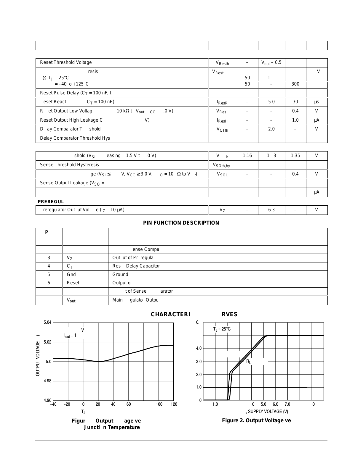
5.04
5.02
5.0
, OUTPUT VOLTAGE (V)
4.98
out
V
Symbol
V
CC
S
i
V
Z
C
T
Gnd
Reset
S
O
V
out
VCC = 14 V
I
= 1.0 mA
out
PIN FUNCTION DESCRIPTION
Description
Supply Voltage
Input of Sense Comparator
Output of Preregulator
Reset Delay Capacitor
Ground
Output of Reset Comparator
Output of Sense Comparator
Main Regulator Output
TYPICAL CHARACTERIZATION CURVES
6.0
5.0
4.0
3.0
2.0
, OUTPUT VOLTAGE (V)
out
V
1.0
T
J
= 25°C
RL = 5.0 k
R
L
= 100 Ω
4.96
-40 -20 0 40 6020 100 120
T
, JUNCTION TEMPERATURE (°C)
J
80
Figure 1. Output Voltage versus
Junction Temperature
http://onsemi.com
0
010
2.0 3.0 4.0 5.0 6.0 7.0 8.0 9.0
1.0
V
, SUPPLY VOLTAGE (V)
CC
Figure 2. Output Voltage versus
Supply Voltage
3
Page 4
L4949, NCV4949
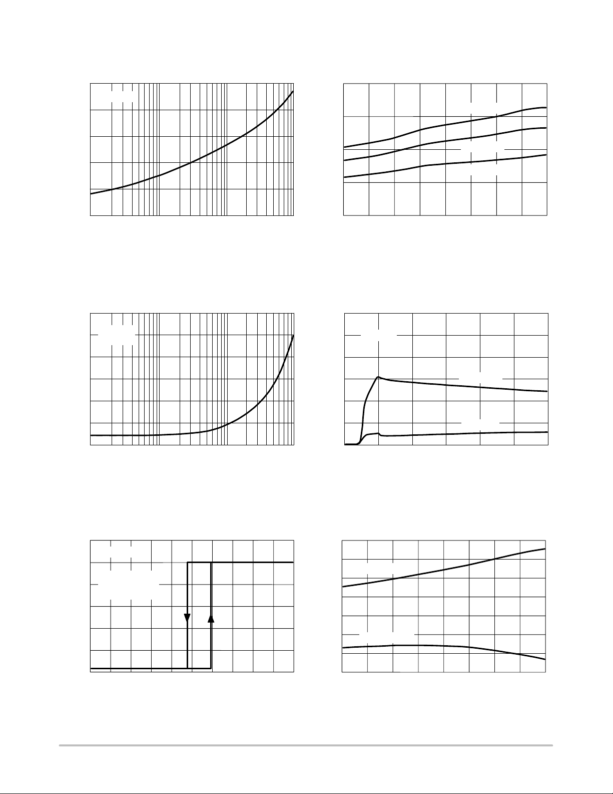
TYPICAL CHARACTERIZATION CURVES (continued)
250
T
= 25°C
J
200
150
100
, DROPOUT VOLTAGE (mV)
50
drop
V
0
0.1 100
I
, OUTPUT CURRENT (mA)
out
101.0
Figure 3. Dropout Voltage versus
Output Current
3.0
VCC = 14 V
2.5
T
= 25°C
J
2.0
0.40
I
= 100 mA
0.30
0.20
, DROPOUT VOLTAGE (mV)
0.10
drop
V
0
-40 -20 0 40 6020 100 120
T
, JUNCTION TEMPERATURE (°C)
J
out
I
out
I
out
= 50 mA
= 10 mA
80
Figure 4. Dropout Voltage versus
Junction Temperature
3.0
T
2.5
2.0
= 25°C
J
1.5
1.0
, QUIESCENT CURRENT (mA)
Q
0.5
I
0
0.1 1.0 10 100
, OUTPUT CURRENT (mA)
I
out
Figure 5. Quiescent Current versus
Output Current
6.0
T
= 25°C
J
5.0
Resistor 10 k
from Reset Output
4.0
to 5.0 V
3.0
, RESET OUTPUT (V)
2.0
Reset
V
1.0
0
4.0 4.1
4.2 4.3 4.4 4.5 4.6 4.7 4.8 4.9 5.0
, OUTPUT VOLTAGE (V)
V
out
Figure 7. Reset Output versus
Regulator Output Voltage
R
1.5
= 100 Ω
L
1.0
, QUIESCENT CURRENT (mA)
Q
0.5
I
0
0 5.0 10 15 20 25 30
, SUPPLY VOLTAGE (V)
V
CC
RL = 5.0 k
Figure 6. Quiescent Current versus
Supply Voltage
4.7
4.66
Upper Threshold
4.62
4.58
4.54
4.5
, RESET THRESHOLD VOLTAGE (V)
Lower Threshold
4.46
Reset
V
4.42
-40 -20
0 20 40 60 80 100 120
T
, JUNCTION TEMPERATURE (°C)
J
Figure 8. Reset Thresholds versus
Junction Temperature
http://onsemi.com
4
Page 5

L4949, NCV4949
TYPICAL CHARACTERIZATION CURVES (continued)
6.0
T
= 25°C
5.0
J
4.0
Resistor 10 k
from Sense Output
to 5.0 V
3.0
2.0
, SENSE OUTPUT VOLTAGE (V)
1.0
SO
V
0
1.0 1.15
1.11.05
1.2 1.25 1.3 1.35 1.4 1.45 1.5
, SENSE INPUT VOLTAGE (V)
V
SI
Figure 9. Sense Output versus
Sense Input Voltage
APPLICATION INFORMATION
Supply Voltage Transient
High supply voltage transients can cause a reset output
signal perturbation. For supply voltages greater than 8.0 V
the circuit shows a high immunity of the reset output against
supply transients of more than 100 V/µs. For supply voltages
1.4
1.38
1.36
1.34
1.32
1.3
1.28
, SENSE INPUT VOLTAGE (V)
1.24
SI
V
1.22
1.2
Upper Threshold
Lower Threshold1.26
-40 -20
0 20 40 60 80 100 120
T
, JUNCTION TEMPERATURE (°C)
J
Figure 10. Sense Thresholds versus
Junction Temperature
less than 8.0 V supply transients of more than 0.4 V/µs can
cause a reset signal perturbation. To improve the transient
behavior for supply voltages less than 8.0 V a capacitor at
Pin 3 can be used. A capacitor at Pin 3 (C3 ≤ 1.0 µF) reduces
also the output noise.
V
out
Reset
C
O
2.0 µA
Sense
C
T
Reset
6
10 kΩ
+
2.0 V
-
R
SO
7
+
1.23 V
-
10 kΩ
V
out
S
o
C3
V
Z
(optional)
V
bat
V
CC
1
C
s
V
S
i
2
CC
Preregulator
Regulator
1.23 V
6.0 V
ref
38 4
NOTES: 1. For stability: Cs ≥ 1.0 µF, CO ≥ 4.7 µF, ESR < 10 Ω at 10 kHz
2. Recommended for application: C
= CO = 10 µF
s
Figure 11. Application Schematic
http://onsemi.com
Gnd
5
5
Page 6

L4949, NCV4949
OPERATING DESCRIPTION
The L4949 is a monolithic integrated low dropout voltage
regulator. Several outstanding features and auxiliary
functions are implemented to meet the requirements of
supplying microprocessor systems in automotive
applications. Nevertheless, it is suitable also in other
applications where the present functions are required. The
modular approach of this device allows the use of other
features and functions independently when required.
Voltage Regulator
The voltage regulator uses an isolated Collector Vertical
PNP transistor as a regulating element. With this structure,
very low dropout voltage at currents up to 100 mA is
obtained. The dropout operation of the standby regulator is
maintained down to 3.0 V input supply voltage. The output
voltage is regulated up to the transient input supply voltage
of 35 V. With this feature no functional interruption due to
overvoltage pulses is generated.
The typical curve showing the standby output voltage as
a function of the input supply voltage is shown in Figure 13.
The current consumption of the device (quiescent current)
is less than 200 µA.
To reduce the quiescent current peak in the undervoltage
region and to improve the transient response in this region,
the dropout voltage is controlled. The quiescent current as
a function of the supply input voltage is shown in Figure 14.
Short Circuit Protection:
The maximum output current is internally limited. In case
of short circuit, the output current is foldback current limited
as described in Figure 12.
10
V
out
V
5.0 V
out
V
CC
Figure 13. Output Voltage versus Supply Voltage
3.0
T
2.5
2.0
1.5
1.0
, QUIESCENT CURRENT (mA)
Q
0.5
I
0
0 5.0 10 15 20 25 30
= 25°C
J
V
, SUPPLY VOLTAGE (V)
CC
R
= 100 Ω
L
RL = 5.0 k
Figure 14. Quiescent Current versus Supply Voltage
35 V5.0 V2.0 V0 V
(V)
5.0
out
V
0
20 100 200
(mA)
I
out
Figure 12. Foldback Characteristic of V
out
Preregulator
To improve the transient immunity a preregulator
stabilizes the internal supply voltage to 6.0 V. This internal
voltage is present at Pin 3 (V
). This voltage should not be
Z
used as an output because the output capability is very small
(≤ 100 µA).
This output may be used as an option when better transient
behavior for supply voltages less than 8.0 V is required. In
this case a capacitor (100 nF – 1.0 µF) must be connected
between Pin 3 and Gnd. If this feature is not used Pin 3 must
be left open.
http://onsemi.com
6
Page 7

L4949, NCV4949
Reset Circuit
The block circuit diagram of the reset circuit is shown in
Figure 15.
The reset circuit supervises the output voltage. The reset
threshold of 4.5 V is defined with the internal reference
voltage and standby output divider.
The reset pulse delay time t
time of an external capacitor C
t
RD
, is defined with the charge
RD
:
T
CTx2.0V
2.0 A
The reaction time of the reset circuit originates from the
discharge time limitation of the reset capacitor CT and is
proportional to the value of CT. The reaction time of the reset
circuit increases the noise immunity.
1.23 V V
ref
Out
Reg
22 k
2.0 µA
C
T
+
-
Figure 15. Reset Circuit
2.0 V
Reset
Standby output voltage drops below the reset threshold
only a bit longer than the reaction time results in a shorter
reset delay time.
The nominal reset delay time will be generated for
standby output voltage drops longer than approximately
50 µs. The typical reset output waveforms are shown in
Figure 16.
V
5.0 V
VRT + 0.1 V
UKT
3.0 V
Reset
out
Switch On Input Drop Dump
V
in
V
out1
t
RD
t
RR
Figure 16. Typical Reset Output Waveforms
Sense Comparator
40 V
t
R
t
RD
Output
Overload
Switch Off
The sense comparator compares an input signal with an
internal voltage reference of typical 1.23 V. The use of an
external voltage divider makes this comparator very flexible
in the application.
It can be used to supervise the input voltage either before
or after the protection diode and to give additional
information to the m icroprocessor like l ow v oltage warnings.
t
http://onsemi.com
7
Page 8

L4949, NCV4949
ORDERING INFORMATION
Device Operating Temperature Range Package Shipping
L4949N DIP–8 50 Units / Rail
L4949D
L4949DR2
NCV4949DR2* SO–8 2500 Units / Tape & Reel
*NCV4949: T
site and change control.
= –40°C, T
low
= +125°C. Guaranteed by design. NCV prefix is for automotive and other applications requiring
high
TJ = –40°C to +125°C
SO–8 98 Units / Rail
SO–8 2500 Units / Tape & Reel
http://onsemi.com
8
Page 9

NOTE 2
–T–
SEATING
PLANE
H
58
–B–
14
F
–A–
C
N
D
G
0.13 (0.005) B
L4949, NCV4949
PACKAGE DIMENSIONS
N SUFFIX
PLASTIC PACKAGE
CASE 626–05
ISSUE L
NOTES:
1. DIMENSION L TO CENTER OF LEAD WHEN
FORMED PARALLEL.
2. PACKAGE CONTOUR OPTIONAL (ROUND OR
SQUARE CORNERS).
3. DIMENSIONING AND TOLERANCING PER ANSI
Y14.5M, 1982.
DIM MIN MAX MIN MAX
A 9.40 10.16 0.370 0.400
B 6.10 6.60 0.240 0.260
C 3.94 4.45 0.155 0.175
D 0.38 0.51 0.015 0.020
L
J
K
M
M
A
T
M
M
F 1.02 1.78 0.040 0.070
G 2.54 BSC 0.100 BSC
H 0.76 1.27 0.030 0.050
J 0.20 0.30 0.008 0.012
K 2.92 3.43 0.115 0.135
L 7.62 BSC 0.300 BSC
M --- 10 --- 10
N 0.76 1.01 0.030 0.040
INCHESMILLIMETERS
http://onsemi.com
9
Page 10

L4949, NCV4949
PACKAGE DIMENSIONS
D SUFFIX
PLASTIC PACKAGE
CASE 751–07
ISSUE W
–Y–
–Z–
–X–
A
58
B
1
S
0.25 (0.010)
4
M
M
Y
K
G
C
SEATING
PLANE
0.10 (0.004)
H
D
0.25 (0.010) Z
M
Y
SXS
N
X 45
M
NOTES:
1. DIMENSIONING AND TOLERANCING PER ANSI
Y14.5M, 1982.
2. CONTROLLING DIMENSION: MILLIMETER.
3. DIMENSION A AND B DO NOT INCLUDE MOLD
PROTRUSION.
4. MAXIMUM MOLD PROTRUSION 0.15 (0.006) PER
SIDE.
5. DIMENSION D DOES NOT INCLUDE DAMBAR
PROTRUSION. ALLOWABLE DAMBAR
PROTRUSION SHALL BE 0.127 (0.005) TOTAL IN
EXCESS OF THE D DIMENSION AT MAXIMUM
MATERIAL CONDITION.
MILLIMETERS
DIMAMIN MAX MIN MAX
4.80 5.00 0.189 0.197
B 3.80 4.00 0.150 0.157
C 1.35 1.75 0.053 0.069
D 0.33 0.51 0.013 0.020
G 1.27 BSC 0.050 BSC
H 0.10 0.25 0.004 0.010
J
J 0.19 0.25 0.007 0.010
K 0.40 1.27 0.016 0.050
M 0 8 0 8
N 0.25 0.50 0.010 0.020
S 5.80 6.20 0.228 0.244
INCHES
http://onsemi.com
10
Page 11

Notes
L4949, NCV4949
http://onsemi.com
11
Page 12

L4949, NCV4949
ON Semiconductor is a trademark and is a registered trademark of Semiconductor Components Industries, LLC (SCILLC). SCILLC reserves the right
to make changes without further notice to any products herein. SCILLC makes no warranty, representation or guarantee regarding the suitability of its products
for any particular purpose, nor does SCILLC assume any liability arising out of the application or use of any product or circuit, and specifically disclaims any
and all liability, including without limitation special, consequential or incidental damages. “Typical” parameters which may be provided in SCILLC data sheets
and/or specifications can and do vary in different applications and actual performance may vary over time. All operating parameters, including “Typicals” must
be validated for each customer application by customer’s technical experts. SCILLC does not convey any license under its patent rights nor the rights of others.
SCILLC products are not designed, intended, or authorized for use as components in systems intended for surgical implant into the body, or other applications
intended to support or sustain life, or for any other application in which the failure of the SCILLC product could create a situation where personal injury or death
may occur. Should Buyer purchase or use SCILLC products for any such unintended or unauthorized application, Buyer shall indemnify and hold SCILLC
and its officers, employees, subsidiaries, affiliates, and distributors harmless against all claims, costs, damages, and expenses, and reasonable attorney fees
arising out of, directly or indirectly, any claim of personal injury or death associated with such unintended or unauthorized use, even if such claim alleges that
SCILLC was negligent regarding the design or manufacture of the part. SCILLC is an Equal Opportunity/Affirmative Action Employer.
PUBLICATION ORDERING INFORMATION
Literature Fulfillment:
Literature Distribution Center for ON Semiconductor
P.O. Box 5163, Denver, Colorado 80217 USA
Phone: 303–675–2175 or 800–344–3860 Toll Free USA/Canada
Fax: 303–675–2176 or 800–344–3867 Toll Free USA/Canada
Email: ONlit@hibbertco.com
N. American Technical Support: 800–282–9855 Toll Free USA/Canada
http://onsemi.com
JAPAN: ON Semiconductor, Japan Customer Focus Center
4–32–1 Nishi–Gotanda, Shinagawa–ku, Tokyo, Japan 141–0031
Phone: 81–3–5740–2700
Email: r14525@onsemi.com
ON Semiconductor Website: http://onsemi.com
For additional information, please contact your local
Sales Representative.
L4949/D
12
 Loading...