

Page 1
KAC-12040
f
4000 (H) x 3000 (V)
CMOS Image Sensor
Description
The KAC−12040 Image Sensor is a high-speed 12 megapixel
CMOS image sensor in a 4/3″ optical format based on a 4.7 mm 5T
CMOS platform. The image sensor features very fast frame rate,
excellent NIR sensitivity, and flexible readout modes with multiple
regions of interest (ROI). The readout architecture enables use of 8, 4,
or 2 LVDS output banks for full resolution readout of 70 frames per
second.
Each LVDS output bank consists of up to 8 differential pairs
operating at 160 MHz DDR for a 320 Mbps data rate per pair.
The pixel architecture allows rolling shutter operation for motion
capture with optimized dynamic range or global shutter for precise
still image capture.
Table 1. GENERAL SPECIFICATIONS
Parameter Typical Value
Architecture 5T Global Shutter CMOS
Resolution 12 Megapixels
Aspect Ratio 4:3
Pixel Size
Total Number of Pixels 4224 (H) × 3192 (V)
Number of Effective Pixels 4016 (H) × 3016 (V)
Number of Active Pixels 4000 (H) × 3000 (V)
Active Image Size 18.8 mm (H) × 14.1 mm (V)
Master Clock Input Speed 5 MHz to 50 MHZ
Maximum Pixel Clock Speed 160 MHz DDR LVDS, 320 Mbps
Number of LVDS Outputs 64 Differential Pairs
Number of Output Banks 8, 4, or 2
Frame Rate, 12 Mp 1−70 fps 10 bits
Charge Capacity 16,000 electrons
Quantum Efficiency
KAC−12040−CBA
KAC−12040−ABA
Read Noise
(at Maximum LVDS Clock)
Dynamic Range 73 dB, Rolling Shutter
Blooming Suppression > 10,000x
Image Lag 1.3 electron
Digital Core Supply 2.0 V
Analog Core Supply 1.8 V
Pixel Supply 2.8 V & 3.5 V
Power Consumption 1.5 W for 12 Mp @ 70 fps 10 bits
Package 267 Pin Ceramic Micro-PGA
Cover Glass AR Coated, 2-sides
NOTE: All Parameters are specified at T = 40°C unless otherwise noted.
4.7 mm (H) × 4.7 mm (V)
23.5 mm (Diagonal), 4/3″ Optical Format
1−75 fps 8 bits
40%, 47%, 45% (470, 540, 620 nm)
53%, 15%, 10% (500, 850, 900 nm)
3.7 e− rms, Rolling Shutter
−
25.5 e
rms, Global Shutter
56 dB, Global Shutter
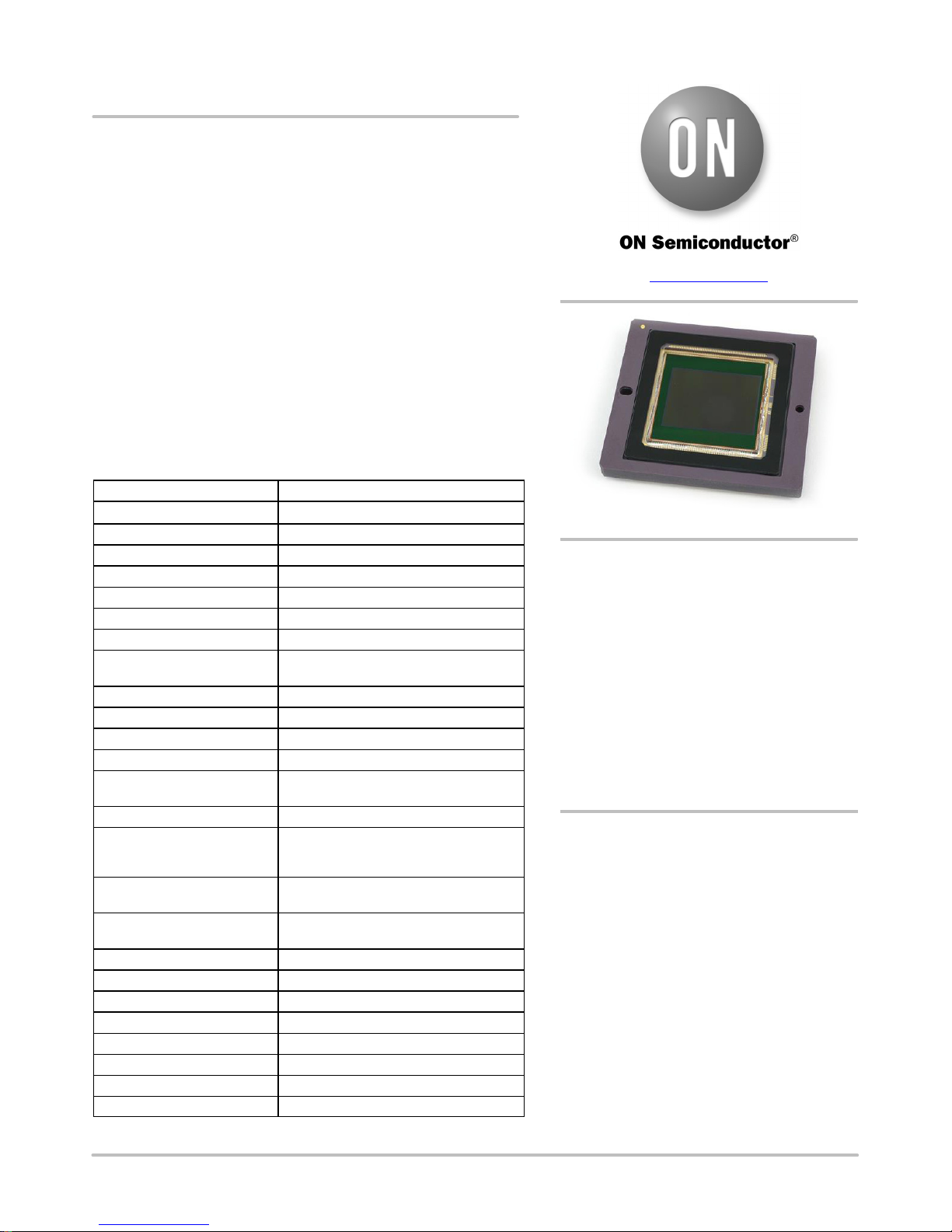
www.onsemi.com
Figure 1. KAC−12040 CMOS Image Sensor
Features
• Global Shutter and Rolling Shutter
• Very Fast Frame Rate
• High NIR Sensitivity
• Multiple Regions of Interest
• Interspersed Video Streams
Applications
• Machine Vision
• Intelligent Transportation Systems
• Surveillance
ORDERING INFORMATION
See detailed ordering and shipping information on page 2 o
this data sheet.
© Semiconductor Components Industries, LLC, 2016
March, 2016 − Rev. 5
1 Publication Order Number:
KAC−12040/D
Page 2

KAC−12040
The image sensor has a pre-configured QFHD (4 × 1080p,
16:9) video mode, fully programmable, multiple ROI for
windowing, programmable sub-sampling, and reverse
readout (flip and mirror). The two ADCs can be configured
clamping, overflow pixel for blooming reduction, black-sun
correction (anti-eclipse), column and row noise correction,
and integrated timing generation with SPI control, 4:1 and
9:1 averaging decimation modes.
for 8-bit, 10-bit, 12-bit or 14-bit conversion and output.
Additional features include interspersed video streams
(dual-video), on-chip responsivity calibration, black
ORDERING INFORMATION
T able 2. ORDERING INFORMATION − KAC−12040 IMAGE SENSOR
Part Number Description Marking Code
KAC−12040−ABA−JD−BA Monochrome, Micro-PGA Package, Sealed Clear Cover Glass with AR
KAC−12040−ABA−JD−AE Monochrome, Micro-PGA Package, Sealed Clear Cover Glass with AR
KAC−12040−CBA−JD−BA Bayer (RGB) Color Filter Pattern, Micro-PGA Package, Sealed Clear Cover
KAC−12040−CBA−JD−AE Bayer (RGB) Color Filter Pattern, Micro-PGA Package, Sealed Clear Cover
1. Engineering Grade samples might not meet final production testing limits, especially for cosmetic defects such as clusters, but also possibly
column and row artifacts. Overall performance is representative of final production parts.
Coating (Both Sides), Standard Grade.
Coating (Both Sides), Engineering Grade.
Glass with AR Coating (Both Sides), Standard Grade.
Glass with AR Coating (Both Sides), Engineering Grade.
KAC−12040−ABA
Serial Number
KAC−12040−CBA
Serial Number
Table 3. ORDERING INFORMATION − EVALUATION SUPPORT
Part Number Description
KAC−12040−CB−A−GEVK Evaluation Hardware for KAC−12040 Image Sensor (Color). Includes Image Sensor.
KAC−12040−AB−A−GEVK Evaluation Hardware for KAC−12040 Image Sensor (Monochrome). Includes Image Sensor.
LENS−MOUNT−KIT−C−GEVK Lens Mount Kit that Supports C, CS, and F Mount Lenses. Includes IR Cut-filter for Color Imaging.
See the ON Semiconductor Device Nomenclature document (TND310/D) for a full description of the naming convention
used for image sensors. For reference documentation, including information on evaluation kits, please visit our web site at
www.onsemi.com
.
www.onsemi.com
2
Page 3
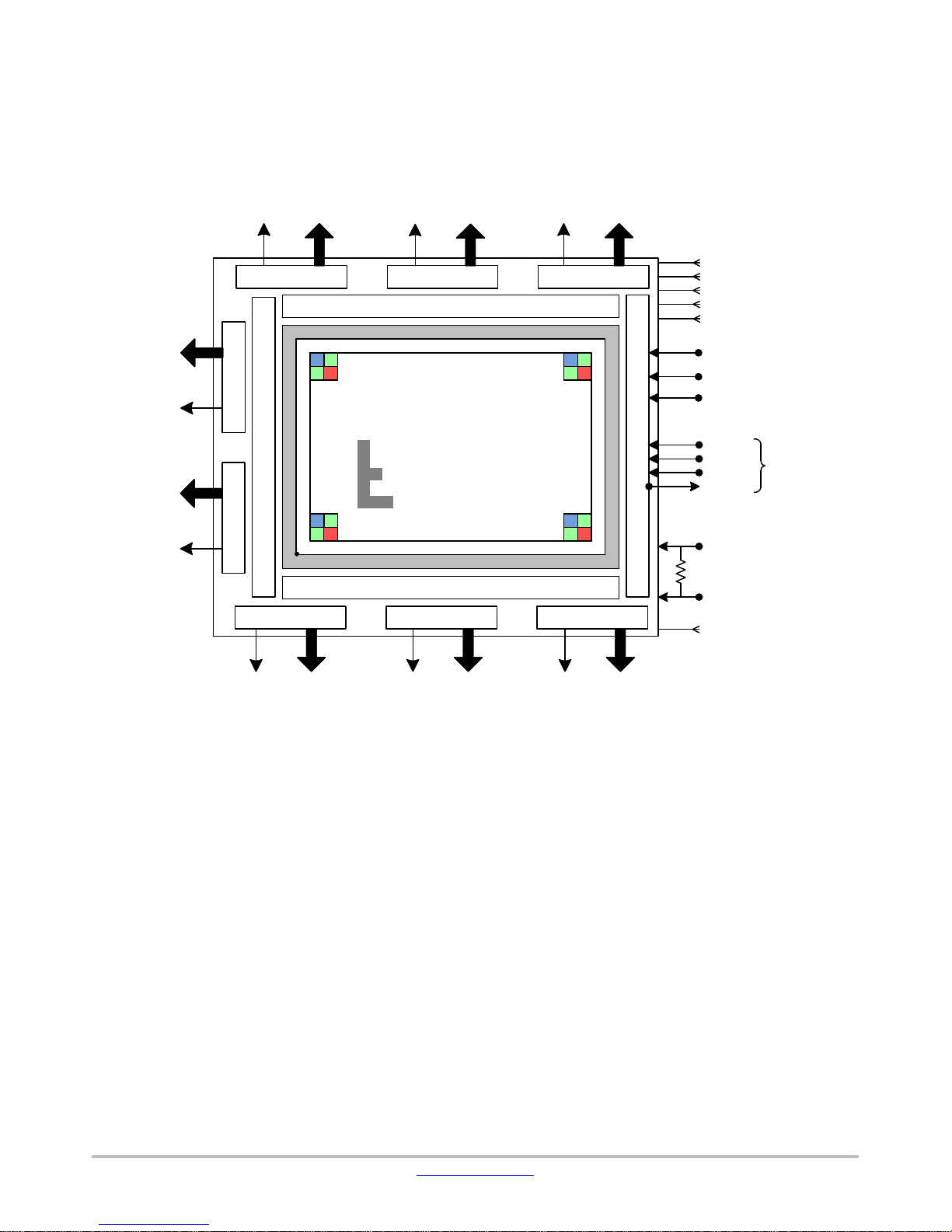
DEVICE DESCRIPTION
Architecture
KAC−12040
1D
0D
− 1D
0
− 0D
0
Clk1
Clk0
6
− 5D
0
5D
Clk7
Clk3
6
− 3D
0
3D
Clk5
LVDS Bank 3 LVDS Bank 5 LVDS Bank 7
Odd Row ADC, Analog Gain, Black-Sun Correction
88
6
B
G
R
G
8
B
G
4000 (H) y 3000 (V)
6
− 7D
0
7D
3.5 V
A
3.3 V
D
2.8 V
A
2.0 V
D
1.8 V
A
G
R
Chip Clock (2 Pins)
TRIGGER
RESETN
4.7 mm Pixel
104
8
8
104
CSN
SCLK
MOSI
6
Digital Gain/Offset, Noise Correction
LVDS Bank 0 LVDS Bank 1
(0, 0)
B
G
R
G
8
88
B
G
R
G
Timing Control, Sub-Sampling/Averaging
Even Row ADC, Analog Gain, Black-Sun Correction
MISO
ADC_Ref1
4.02 kW ±1%
ADC_Ref2
Serial
Peripheral
Interface
(SPI)
LVDS Bank 2 LVDS Bank 4 LVDS Bank 6
VSS 0 V
Clk2
6
− 2D
0
2D
6
Clk4
− 4D
0
4D
Figure 2. Block Diagram
Clk6
6
− 6D
0
6D
www.onsemi.com
3
Page 4
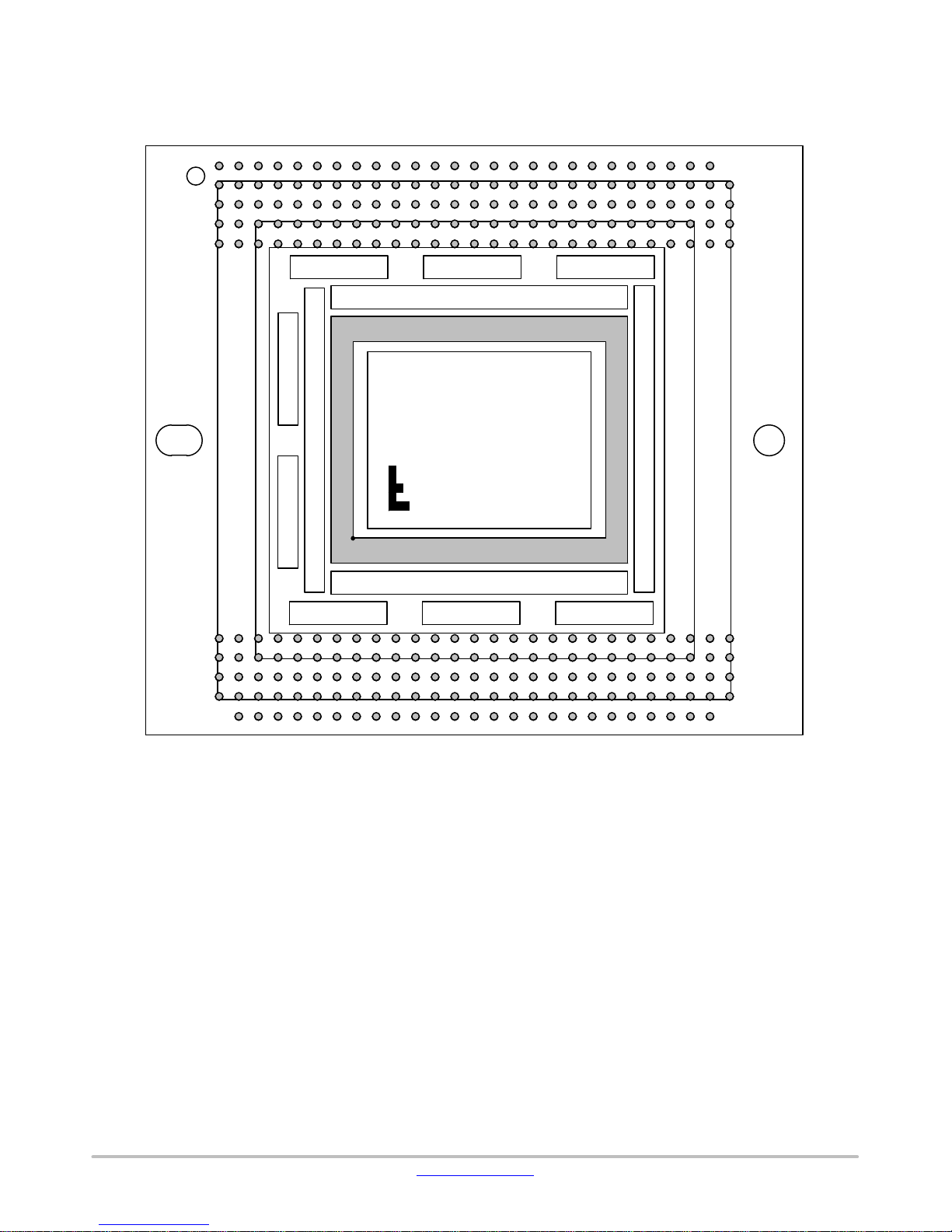
Physical Orientation
272625242322212019181716151413121110987654321
KAC−12040
A
B
C
D
E
LVDS Bank 3 LVDS Bank 5 LVDS Bank 7
LVDS Bank 0 LVDS Bank 1
LVDS Bank 2 LVDS Bank 4 LVDS Bank 6
Notes:
1. The center of the pixel array is aligned to the physical package center.
2. The region under the sensor die is clear of pins enabling the use of a heat sink.
3. Non-symmetric mounting holes provide orientation and mounting precision.
4. Non-symmetric pins prevent incorrect placement in PCB.
5. Letter “F” indicator shows default readout direction relative to package pin 1.
Figure 3. Package Pin Orientation − Top X-Ray View
AA
AB
AC
AD
AE
272625242322212019181716151413121110987654321
www.onsemi.com
4
Page 5
KAC−12040
Table 4. PRIMARY PIN DESCRIPTION
Pin Name Type Description
AB09 RESETN DI Sensor Reset (0 V = Reset State)
E07 CLK_In1 DI Sensor Input Clk_In1 (45−50 MHz)
D08 CLK_In2 DI Sensor Input Clk_In2 (Connect to Clk1)
AB08 TRIGGER DI Trigger Input (Optional)
AA05 SCLK DI SPI Master Clock
AA08 MOSI DI SPI Master Output, Slave Input
AA07 MISO DO SPI Master Input, Slave Output
AA06 CSN DI SPI Chip Select (0 V = Selected)
AA14 ADC_Ref1 AO
AA15 ADC_Ref2 AO
AB07 MSO DO Mechanical Shutter Output Sync (Optional)
AB06 FLO DO Flash Output Sync (Optional)
E05 FEN DO Frame Enable Reference Output (Optional)
E06 LEN DO Line Enable Reference Output (Optional)
1. DI = Digital Input, DO = Digital Output, AO = Analog Output.
2. Tie unused DI pins to Ground, NC unused DO pins.
3. By default Clk_In2 should equal Clk_In1 and should be the same source clock.
4. The RESETN pin has a 62 kW internal pull-up resistor, so if left floating the chip will not be in reset mode.
5. The TRIGGER pin has an internal 100 kW pull down resistor. If left floating (and at default polarity) then the sensor state will not be affected
by this pin (i.e. defaults to ‘not triggered’ mode if floated).
6. All of the DI and DO pins nominally operate at 0 V → 2.0 V and are associated with the VDD_DIG power supply.
4.02 kW ±1% Resistor between Ref1 & Ref2
4.02 kW ±1% Resistor between Ref1 & Ref2
Table 5. POWER PIN DESCRIPTION
Name Voltage Pins Description
VDD_LVDS 3.3 V D C04, C05, C23, C24, D04, D24, E04, E24, AA04, AA24,
AB04, AB24, AC04, AC05 AC23, AC24
VDD_DIG 2.0 V D C18, C19, D18, D19, E18, AA18, AB18, AB19, AC18, AC19,
C20, C21, C22, D20, D21, D22, D23, E20, E21, E22, AA20,
AA21, AA22, AB20, AB21, AB22, AB23, AC20, AC21,
AC22, AB15, E08
AVDD_HV 3.5 V A C11, D11, E11, AA11, AB11, AC11, C10, D10, E10, AA10,
AB10, AC10
Vref_P 2.8 V A C13, D13, E13, AA13, AB13, AC13 Pixel Supply 2
AVDD_LV 1.8 V A C17, D16, D17, E17, AA17, AB16, AB17, AC17 Analog Low Voltage Supply
Vpixel_low 0 V E09 Pixel Supply 3. Combine with VSS for
VSS 0 V C12, C14, D12, D14, E12, AA12, AB12, AB14, AC12, AC14,
E15, D15, AA09, A02, A14, A26, B14, C03, C06, C25, D03,
D25, E03, E19, E23, E25, AA03, AA19, AA23, AA25, AB25,
AC03, AC06, AC25, AD14, AE02, AE14, AE26
No Connect NA A01, AC09, E14, E16, C09, D09, D05, D06, D07, AA16,
AB05
LVDS Output Supply
Digital Core Supply
Pixel Supply 1
normal operation. Can be pulsed for
Extended Dynamic Range Operation.
Sensor Ground Reference
Unused and test-only pins. These
pins must be floated.
www.onsemi.com
5
Page 6
Table 6. L VDS PIN DESCRIPTION
KAC−12040
Pin Name Description
E01
1DCLK+
E02 1DCLK−
D01 1DATA0+
D02 1DATA0−
C01 1DATA1+
C02 1DATA1−
B01 1DATA2+
B02 1DATA2−
A03 1DATA3+
B03 1DATA3−
A04 1DATA4+
B04 1DATA4−
A05 1DATA5+
B05 1DATA5−
A06 1DATA6+
B06 1DATA6−
Pin Name Description
0DCLK+
AA01
AA02 0DCLK−
AB01 0DATA0+
AB02 0DATA0−
AC01 0DATA1+
AC02 0DATA1−
AD01 0DATA2+
AD02 0DATA2−
AE03 0DATA3+
AD03 0DATA3−
AE04 0DATA4+
AD04 0DATA4−
AE05 0DATA5+
AD05 0DATA5−
AE06 0DATA6+
AD06 0DATA6−
Bank 1
LVDS Clock
Bank 1
LVDS Data
Bank 0
LVDS Clock
Bank 0
LVDS Data
Pin Name Description
C07
3DCLK+
C08 3DCLK−
A07 3DATA0+
B07 3DATA0−
A08 3DATA1+
B08 3DATA1−
A09 3DATA2+
B09 3DATA2−
A10 3DATA3+
B10 3DATA3−
A11 3DATA4+
B11 3DATA4−
A12 3DATA5+
B12 3DATA5−
A13 3DATA6+
B13 3DATA6−
Pin Name Description
2DCLK+
AC07
AC08 2DCLK−
AE07 2DATA0+
AD07 2DATA0−
AE08 2DATA1+
AD08 2DATA1−
AE09 2DATA2+
AD09 2DATA2−
AE10 2DATA3+
AD10 2DATA3−
AE11 2DATA4+
AD11 2DATA4−
AE12 2DATA5+
AD12 2DATA5−
AE13 2DATA6+
AD13 2DATA6−
Bank 3
LVDS Clock
Bank 3
LVDS Data
Bank 2
LVDS Clock
Bank 2
LVDS Data
Pin Name Description
C15
5DCLK+
C16 5DCLK−
A15 5DATA0+
B15 5DATA0−
A16 5DATA1+
B16 5DATA1−
A17 5DATA2+
B17 5DATA2−
A18 5DATA3+
B18 5DATA3−
A19 5DATA4+
B19 5DATA4−
A20 5DATA5+
B20 5DATA5−
A21 5DATA6+
B21 5DATA6−
Pin Name Description
4DCLK+
AC15
AC16 4DCLK−
AE15 4DATA0+
AD15 4DATA0−
AE16 4DATA1+
AD16 4DATA1−
AE17 4DATA2+
AD17 4DATA2−
AE18 4DATA3+
AD18 4DATA3−
AE19 4DATA4+
AD19 4DATA4−
AE20 4DATA5+
AD20 4DATA5−
AE21 4DATA6+
AD21 4DATA6−
Bank 5
LVDS Clock
Bank 5
LVDS Data
Bank 4
LVDS Clock
Bank 4
LVDS Data
Pin Name Description
A22
7DCLK+
B22 7DCLK−
A23 7DATA0+
B23 7DATA0−
A24 7DATA1+
B24 7DATA1−
A25 7DATA2+
B25 7DATA2−
B27 7DATA3+
B26 7DATA3−
C27 7DATA4+
C26 7DATA4−
D27 7DATA5+
D26 7DATA5−
E27 7DATA6+
E26 7DATA6−
Pin Name Description
6DCLK+
AE22
AD22 6DCLK−
AE23 6DATA0+
AD23 6DATA0−
AE24 6DATA1+
AD24 6DATA1−
AE25 6DATA2+
AD25 6DATA2−
AD26 6DATA3+
AD27 6DATA3−
AC26 6DATA4+
AC27 6DATA4−
AB26 6DATA5+
AB27 6DATA5−
AA26 6DATA6+
AA27 6DATA6−
Bank 7
LVDS Clock
Bank 7
LVDS Data
Bank 6
LVDS Clock
Bank 6
LVDS Data
1. All LVDS Data and Clock lines must be routed with 100 W differential transmission line traces.
2. All the traces for a single LVDS Bank should be the same physical length to minimize skew between the clock and data lines.
3. In 2 Bank mode, only LVDS banks 0 and 1 are active.
4. In 4 Bank mode, only LVDS bank 0, 1, 2, and 3 are active.
5. Float the pins of unused LVDS Banks to conserve power.
6. Unused pins in active banks (due to ADC bit depth < 14) are automatically tri-stated to save power, but these can also be floated.
www.onsemi.com
6
Page 7
KAC−12040
IMAGING PERFORMANCE
Table 7. TYPICAL OPERATIONAL CONDITIONS
(Unless otherwise noted, the Imaging Performance Specifications are measured using the following conditions.)
Description
Light Source Continuous Red, Green and Blue LED Illumination 1
Temperature Measured Die Temperature: 40°C and 27°C
Integration Time 16.6 ms (1400d LL, Register 0201h)
Readout Mode Dual-Scan, Global Shutter, 320 MHz, PLL2
Clamps Column/Row Noise Corrections Active, Frame Black Level Clamp Active
ADC Bit Depth 10 bit
Analog Gain Unity Gain or Referred Back to Unit Gain
1. For monochrome sensor, only green LED used.
T able 8. KAC−12040−ABA CONFIGURATION (MONOCHROME)
Wavelength
Description Symbol
Peak Quantum Efficiency
Green
NIR1
NIR2
Responsivity − 84 −
Responsivity − 7.0 −
QE
MAX
(nm)
550
850
900
Condition Notes
Temperature
Min. Nom. Max. Unit
−
−
−
53
15
10
−
−
−
% Design 27
ke
Lux @ s
V
Lux @ s
*
Sampling
Plan
Design 27 20
Design 27 21
Tested at
(5C)
Test
T able 9. KAC−12040−CBA CONFIGURATION (BAYER RGB)
Wavelength
Description Symbol
Peak Quantum Efficiency
Green
NIR1
NIR2
Responsivity Blue
Responsivity Blue
QE
MAX
(nm)
470
540
620
850
900
Green
Red
Green
Red
Min. Nom. Max. Unit
−
−
−
−
−
−
−
−
−
−
−
40
47
45
15
10
17
35
38
1.4
2.9
3.2
Sampling
Plan
−
−
−
−
−
−
−
−
−
−
−
% Design 27
*
ke
Lux @ s
V
Lux @ s
Design 27 20
Design 27 21
Temperature
Tested at
(5C)
Test
www.onsemi.com
7
Page 8

KAC−12040
Table 10. PERFORMANCE SPECIFICATIONS ALL CONFIGURATIONS
Description Symbol Min. Nom. Max. Unit
Photodiode Charge
Capacity
PNe − 16 − ke
−
Sampling
Plan
Tested at
(5C)
Die 27, 40 16
Temperature
Test Notes
Read Noise ne−T −
Total Pixelized Noise −
Dynamic Range DR −
Column Noise C
Row Noise R
Dark Field Local
N
N
DSNU_flr −
Non-Uniformity Floor
Bright Field Global
PRNU_1 − 1.5 − % rms Die 27, 40 2 2
3.7 RS
−
25.5 GS
4.5 RS
−
28.3 GS
73 RS
−
56 GS
−
0.6 RS
−
3.0 GS
−
1.0 RS
−
5.0 GS
3.0 RS
−
21 GS
−
e− rms Die 27 8 1
−
−
e− rms Die 27 19 1
−
−
dB Die 27 1, 4
−
−
e− rms Die 27 9 1, 6
−
−
e− rms Die 27 10 1, 7
−
−
e− rms Die 27, 40 1 1, 5
−
Photoresponse
Non-Uniformity
Bright Field Global Peak to
PRNU_2 − 6.5 − % pp Die 27, 40 3 2
Peak Photoresponse
Non-Uniformity
Maximum Photoresponse
NL − 6.3 − % Die 27, 40 11 3
Non-Linearity
Maximum Gain Difference
DG
− 0.3 − % Die 27, 40 12 8
between Outputs
Photodiode Dark Current I
Storage Node Dark Current I
PD
VD
Image Lag Lag − 1.3 10
Black-Sun Anti-Blooming X
AB
− 4.6 70 e/p/s Die 40 13 9
− 1,200 5,000 e/p/s Die 40 14 5
−
−
−
12
> 10,000
−
W/cm
−
xllumSat
Design 27, 40 15
2
Design 27 7 14
Parasitic Light Sensitivity PLS − 730 − − Design 27 6 10
Dual-Video WDR −
Pulsed Pixel WDR
140 RS
−
120 GS
−
dB Design 27 1, 11,
−
− 100 − dB Design 27 12, 13
(GS Only)
1. RS = Rolling Shutter Operation Mode, GS = Global Shutter Operation Mode.
2. Measured per color, worst of all colors reported.
3. Value is over the range of 10% to 90% of photodiode saturation, Green response used.
4. Uses 20LOG (PNe / ne
−
T).
5. Photodiode dark current made negligible.
6. Column Noise Correction active.
7. Row Noise Correction active.
8. Measured at ~70% illumination.
9. Storage node dark current made negligible.
10.GSE (Global Shutter Efficiency) = 1 −1 / PLS.
11.Min vs Max integration time at 30 fps.
12.WDR measures expanded exposure latitude from linear mode DR.
13.Min/Max responsivity in a 30 fps image.
14.Saturation Illumination referenced to a 3 line time integration.
12
www.onsemi.com
8
Page 9
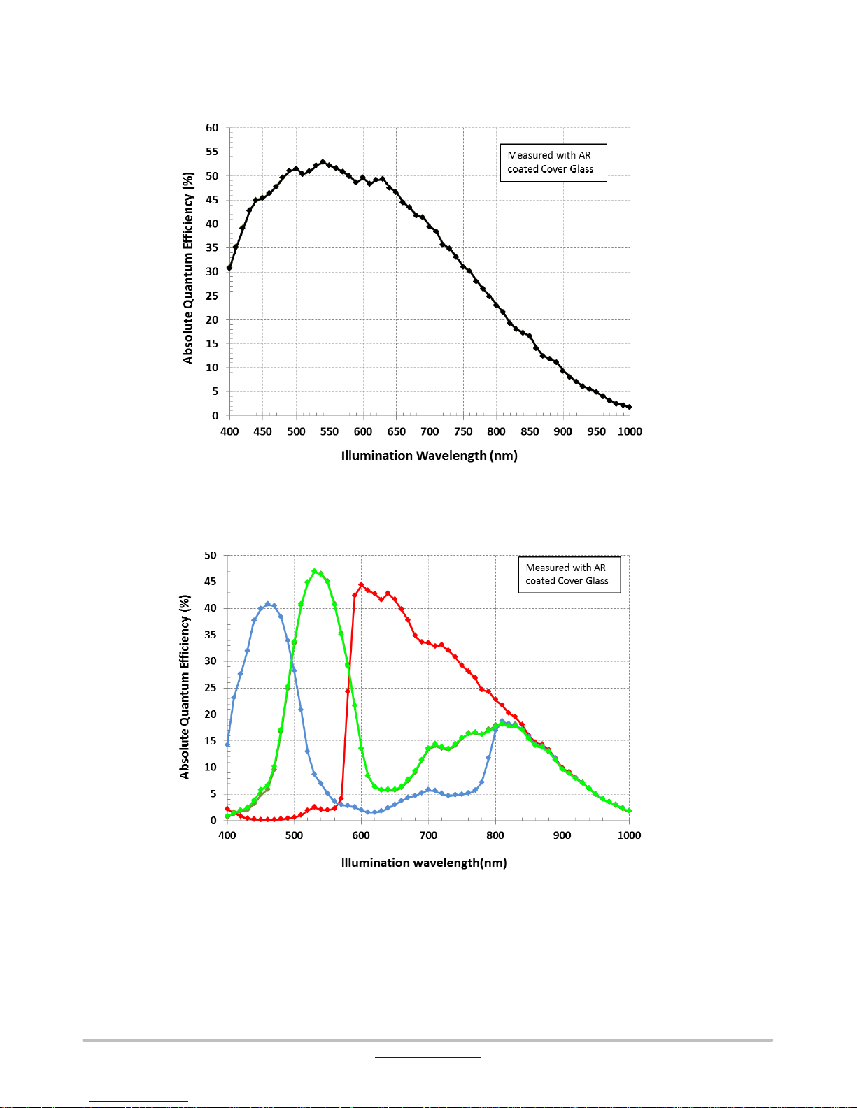
TYPICAL PERFORMANCE CURVES
KAC−12040
Figure 4. Monochrome QE (with Microlens)
Figure 5. Bayer QE (with Microlens)
www.onsemi.com
9
Page 10
KAC−12040
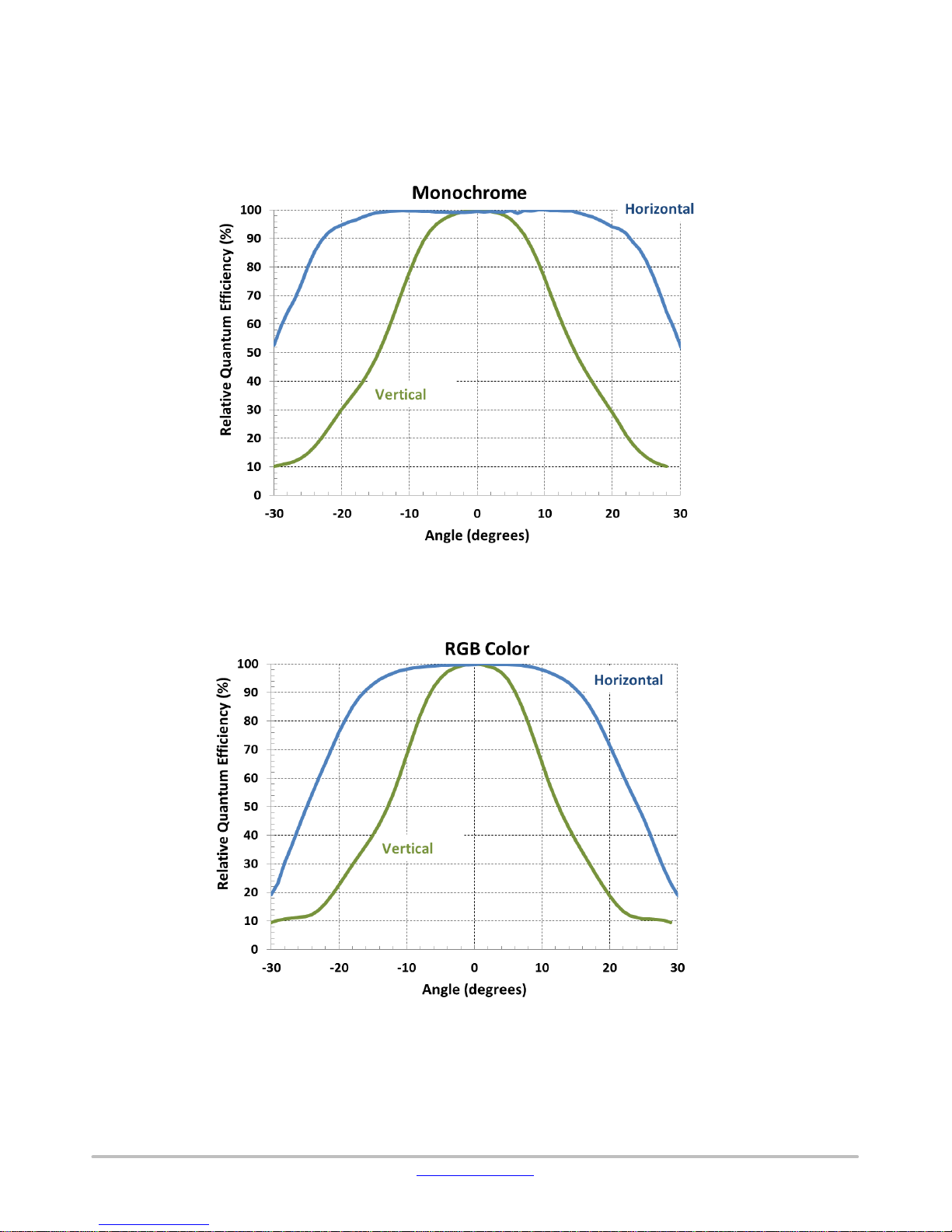
Angular Quantum Efficiency
For the curves marked “Horizontal”, the incident light angle is varied along the wider array dimension.
For the curves marked “Vertical”, the incident light angle is varied along the shorter array dimension.
Figure 6. Monochrome Relative Angular QE (with Microlens)
Figure 7. Bayer Relative Angular QE (with Microlens)
www.onsemi.com
10
Page 11
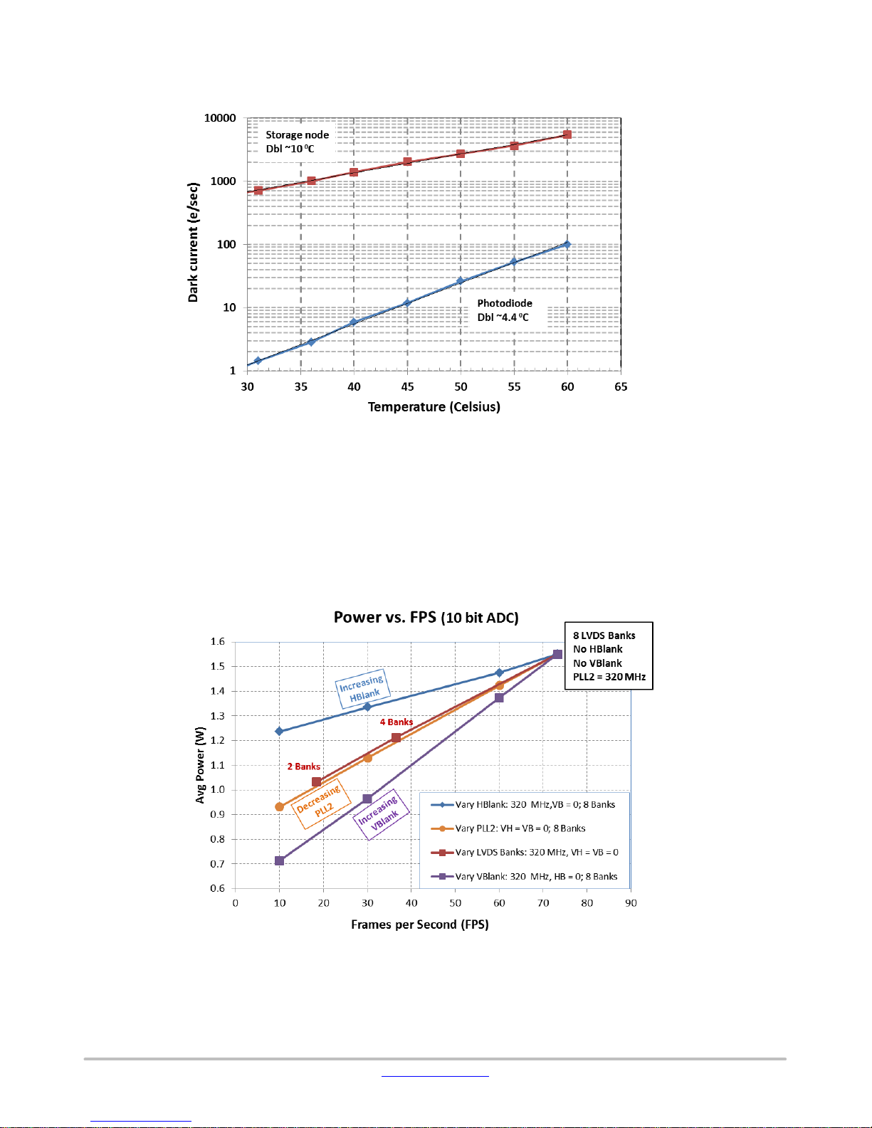
Dark Current vs. Temperature
NOTE: “Dbl” denotes an approximate doubling temperature for the dark current for the displayed temperature range.
KAC−12040
Figure 8. Dark Current vs. Temperature
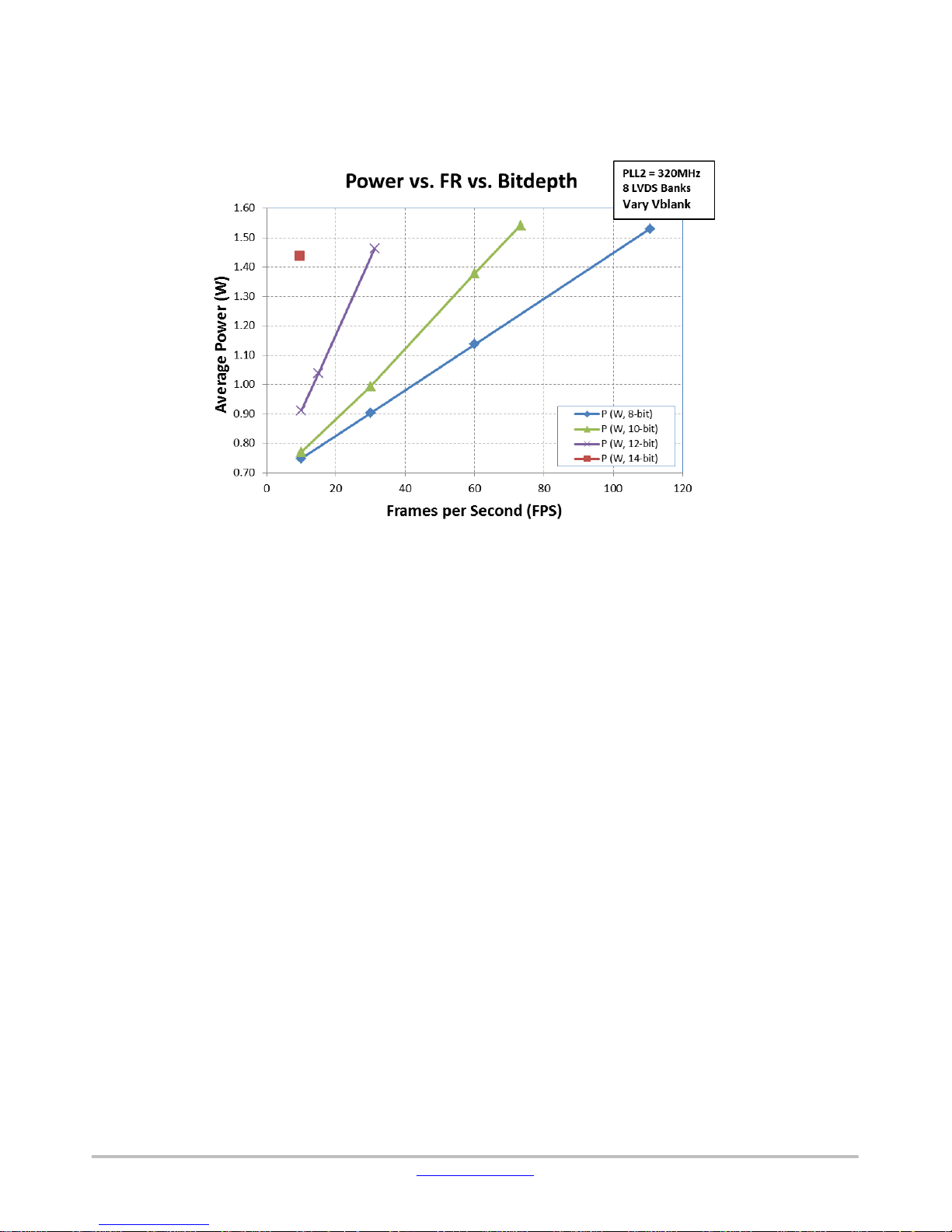
Power vs. Frame Rate
The most effective method to use the maximum PLL2
speed (313 → 320 MHz) and control frame rate with
minimum Power and maximum image quality is to adjust
Vertical Blanking. (register 01F1h). Unnecessary chip
operations are suspended during Vertical Blanking
conserving significant power consumption and also
minimizing the image storage time on the storage node when
in Global Shutter Operation.
NOTE: The LVDS clock is ½ the PLL2 clock speed.
Figure 9. Power vs. Frame Rate, 10 bit Mode
www.onsemi.com
11
Page 12
KAC−12040
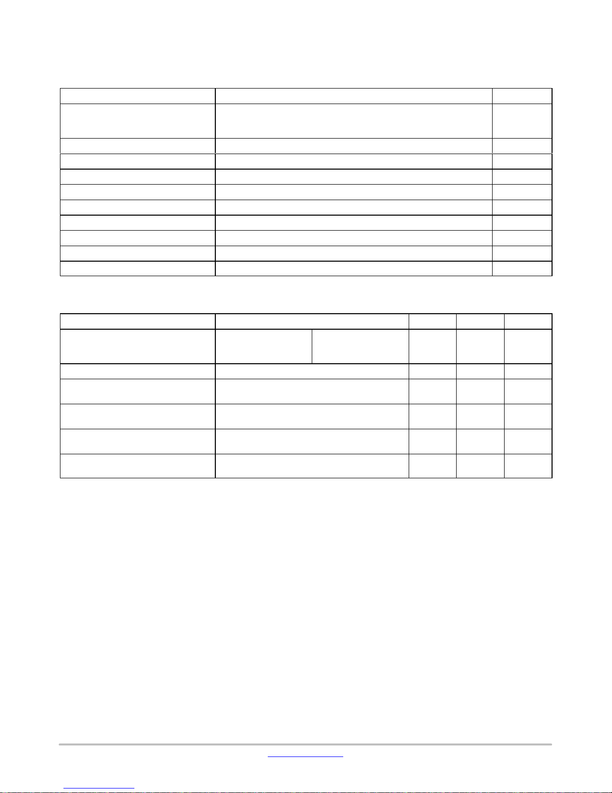
Power and Frame Rate vs. ADC Bit Depth
Increasing the ADC bit depth impacts the frame rate by
changing the ADC conversion time. The following figure
shows the power and Frame rate range for several typical
cases.
Figure 10. ADC Bit Depth Impact on Frame Rate and Power
www.onsemi.com
12
Page 13
KAC−12040
DEFECT DEFINITIONS
Table 11. OPERATION CONDITIONS FOR DEFECT TESTING
Description Condition Notes
Operational Mode 10 bit ADC, 8 LVDS Outputs, Global Shutter and Rolling Shutter Modes,
Pixels per Line 4,000
Lines per Frame 3,000
Line Time
Frame Time 13.9 ms
Photodiode Integration Time 33 ms
Storage Readout Time 13.9 ms
Temperature 40°C and 29°C
Light Source Continuous Red, Green and Blue LED Illumination 1
Operation Nominal Operating Voltages and Timing, PLL1 = 320 MHz, Wafer Test
1. For monochrome sensor, only the green LED is used.
Table 12. DEFECT DEFINITIONS FOR TESTING
Description Definition Limit Test Notes
Dark Field Defective Pixel 30°C
Bright Field Defective Pixel Defect ≥ ±12% from Local Mean 120 5 2, 5
Cluster Defect A group of 2 to 10 contiguous defective pixels, but
Column/Row Major Defect A group of more than 10 contiguous defective pixels
Dark Field Faint Column/Row Defect RS: 3 dn Threshold
Bright Field Faint Column/Row Defect RS: 12 dn Threshold
1. RS = Rolling Shutter, GS = Global Shutter.
2. For the color devices, all bright defects are defined within a single color plane, each color plane is tested.
3. Cluster defects are separated by no less than two good pixels in any direction.
4. Rolling Shutter Dark Field points are dominated by photodiode integration time, Global Shutter Dark Field defects are dominated by the
readout time.
5. The net sum of all bright and dark field pixel defects in rolling and global shutter are combined and then compared to the test limit.
Dual-Scan, Black Level Clamp ON, Column/Row Noise Corrections ON,
1× Analog Gain, 1× Digital Gain
8.7 ms
RS: Defect ≥ 20 dn
GS: Defect ≥ 180 dn
no more than 3 adjacent defects horizontally.
along a single column or row.
GS: 10 dn Threshold
GS: 18 dn Threshold
40°C
RS: Defect ≥ 30 dn
GS: Defect ≥ 240 dn
120 4 1, 4, 5
22 3
0
0 17 1
0 18 1
Defect Map
The defect map supplied with each sensor is based upon
testing at an ambient (29°C) temperature. All defective
pixels are reference to pixel (0, 0) in the defect maps. See
Figure 11 for the location of pixel (0, 0).
www.onsemi.com
13
Page 14

KAC−12040
TEST DEFINITIONS
Test Regions of Interest
Image Area ROI: Pixel (0, 0) to Pixel (4015, 3015)
Active Area ROI: Pixel (8, 8) to Pixel (3999, 2999)
Center ROI: Pixel (1958, 1458) to Pixel (2057, 1557)
Only the Active Area ROI pixels are used for performance and defect tests.
B
G
R
G
4000 (H) y 3000 (V)
4.7 mm Pixel
0,0
8,8
104
8
88
8
8
88
B
G
R
G
8
104
B
G
R
G
Figure 11. Regions of Interest
Test Descriptions
1) Dark Field Local Non-Uniformity Floor (DSNU_flr)
This test is performed under dark field conditions.
A 4 frame average image is collected. This image is
partitioned into 300 sub-regions of interest, each of which is
200 by 200 pixels in size. For each sub-region the standard
deviation of all its pixels is calculated. The dark field local
non-uniformity is the largest standard deviation found from
all the sub regions of interest. Units: e
−
rms (electrons rms).
2) Bright Field Global Photoresponse Non-Uniformity
(PRNU_1)
The sensor illuminated to 70% of saturation (~700 dn). In
this condition a 4 frame average image is collected. From
this 4 frame average image a 4 frame average dark image is
subtracted. The Active Area Standard Deviation is the
standard deviation of the resultant image and the Active
Area Signal is the average of the resultant image.
PRNU_1 + 100 @
Units : % rms
ǒ
Active Area Signal
Ǔ
Active Area Standard Deviation
3) Bright Field Global Peak to Peak Non-Uniformity
(PRNU_2)
This test is performed with the sensor uniformly
illuminated to 70% of saturation (~700 dn), a 4 frame
average image is collected and a 4 frame averaged dark
image is subtracted. The resultant image is partitioned into
300 sub regions of interest, each of which is 200 by
200 pixels in size. The average signal level of each sub
regions of interest (sub-ROI) is calculated.
The highest sub-ROI average (Maximum Signal) and the
lowest sub-ROI average (Minimum Signal) are then used in
the following formula to calculate PRNU_2.
PRNU_2 + 100 @
Units : % pp
ǒ
Active Area Signal
Ǔ
Max. Signal * Min. Signal
4) Dark Field Defect Test
This test is performed under dark field conditions.
The sensor is partitioned into 300 sub regions of interest,
each of which is 128 by 128 pixels in size. In each region of
interest, the median value of all pixels is found. For each
region of interest, a pixel is marked defective if it is greater
than or equal to the median value of that region of interest
plus the defect threshold specified in the Defect Definition
Table section.
5) Bright Field Defect Test
This test is performed with the imager illuminated to
a level such that the output is at approximately 700 dn.
The average signal level of all active pixels is found.
The bright and dark thresholds are set as:
Dark Defect Threshold = Active Area Signal ⋅ Threshold
Bright Defect Threshold = Active Area Signal ⋅ Threshold
The sensor is then partitioned into 300 sub regions of
interest, each of which is 128 by 128 pixels in size. In each
region of interest, the average value of all pixels is found.
For each region of interest, a pixel is marked defective if it
is greater than or equal to the median value of that region of
interest plus the bright threshold specified or if it is less than
www.onsemi.com
14
Page 15

KAC−12040
or equal to the median value of that region of interest minus
the dark threshold specified.
Example for bright field defective pixels:
• Average value of all active pixels is found to be 700 dn
• Lower defect threshold: 700 dn ⋅ 12% = 84 dn
• A specific 128 × 128 ROI is selected:
♦ Median of this region of interest is found to be
690 dn.
♦ Any pixel in this region of interest that is
≤ (690 − 84 dn) in intensity will be marked
defective.
♦ Any pixel in this region of interest that is
≥ (690 − 84 dn) in intensity will be marked
defective.
• All remaining 299 sub regions of interest are analyzed
for defective pixels in the same manner.
6) Parasitic Light Sensitivity (PLS)
Parasitic Light Sensitivity is the ratio of the light
sensitivity of the photodiode to the light sensitivity of the
storage node in Global Shutter. There is no equivalent
distortion in Rolling Shutter. A low PLS value can provide
distortion of the image on the storage node by the scene
during readout.
PLS +
GSE (Global Shutter Efficiency) is a related unit.
Detailed Method: Photodiode Responsivity:
The sensor is set in global shutter serial mode (integration
time not overlapping readout) and the FLO signal is used to
control a 550 nm normal incident (or large f# focused)
illumination source so that the sensor is illuminated only
during photodiode integration time (not illuminated during
readout time). The integration time is not critical but should
be large enough to create a measurable mean during this
time. A 16 frame-average illuminated photodiode image is
recorded. A 16 frame-average dark frame using the same
sensor settings is captured and is subtracted from the
illuminated image.
Detailed Method: Storage Node Responsivity:
The sensor is set to a special characterization mode where
the PD signal is discarded and does not impact the storage
node. A long total frame time (storage node exposure time)
is used to increase the storage node signal. A 16
frame-average dark frame is captured. The sensor is
illuminated by the same 550 nm incident light source used
for the photodiode responsivity. A 16 frame-average
illuminated photodiode image is recorded; the dark frame
image is subtracted from this. The integration time is not
critical but should be set such that a significant response is
detected, typically several orders of magnitude greater than
the photodiode integration time.
Photodiode Responsivity
Storage Node Responsivity
GSE +ǒ1 *
1
PLS
(UnitlessRatio)
Ǔ
%
7) Black-Sun Anti-Blooming
A typical CMOS image sensor has a light response profile
that goes from 0 dn to saturation (1023 dn for KAC−12040
in 10 bit ADC mode) and, with enough light, back to 0 dn.
The sensor reaching 0 dn at very bright illumination is often
called the “Black-sun” artifact and is undesirable. Black-sun
artifact is typically the dominant form of anti-blooming
image distortion. For the KAC−12040 the Black-sun artifact
threshold is measured at the onset of saturation distortion,
not at the point where the output goes to 0 dn. To first order
the onset of black-sun artifact for the KAC−12040 is not
proportional to the integration time or readout time.
The sensor is placed in the dark at unity gain and
illuminated with a 532 nm laser with the intensity of about
26 W/cm
2
at the center of the sensor. The laser is strong
enough to make the center of the laser spot below 1020 dn
without any ND filters. ND filters are added to adjust the
laser intensity until the signal in the region at the center of
the spot increases to > 1020 dn.
This illumination intensity at this ND filter is recorded
2
(W/cm
) as the Black-Sun Anti-blooming.
The ‘xIlumSat’ unit is calculated using and integration
time of 100 msec.
Exposing the sensor to very strong illumination for
extended periods of time will permanently alter the sensor
performance in that localized region.
8) Read Noise
This test is performed with no illumination and one line of
integration time. The read noise is defined as one standard
deviation of the frequency histogram containing the values
of all pixels after the excessively deviant pixels (± three
standard deviations) are removed.
9) Column Noise
After all rows are averaged together. Shading (low
frequency change wrt column address) is removed.
A frequency histogram is constructed of the resulting
column values. The column noise is the standard deviation
of the frequency histogram of the column values.
10) Row Noise
All columns are averaged together. Shading (low
frequency change wrt row address) is removed. A frequency
histogram is constructed of the resulting row values.
The row noise is the standard deviation of the frequency
histogram of the row values.
11) Maximum Photoresponse Non-Linearity
The photoresponse non-linearity is defined as the
deviation from the best fit of the sensor response using 70%
of saturation and zero signal as the reference points.
The different signal levels are determined by varying the
integration time. The sensor saturation level is (1023-dark
offset). The dark offset is subtracted from the image for the
following M
AVG
and L
AVG
.
www.onsemi.com
15
Page 16

KAC−12040
• The integration time is varied until the integration time
required to reach the 70% saturation is determined.
M
= the active array mean at the 70% saturation
AVG
integration time.
• The integration is set to 1/14 (5% exposure point).
= meant at the 5% exposure point.
L
AVG
• PRNL (@ 5% saturation) = ((L
AVG/MAVG
⋅ 100
12) Maximum Gain Difference between Outputs
The sensor contains two ADC and four channels of analog
data in its highest frame rate configuration. The sensor is
factory calibrated to reduce the gain differences between the
channels. The gain variations are manifest as a row oriented
pattern where every other row uses a different ADC. Using
triple scan read out mode, an additional two analog channels
are introduced resulting in a four row pattern. With one
channel (‘Top Ping’) used as the reference, the residual gain
difference is defined as:
Bottom Ping Row Average
ǒ
Top Ping Row Average
Top Pong Row Average
ǒ
Top Ping Row Average
Bottom Pong Row Average
ǒ
Top Ping Row Average
* 1Ǔ@ 100
* 1Ǔ@ 100
* 1Ǔ@ 100
13) Photodiode Dark Current
The photodiode dark current is measured in rolling shutter
read out mode using 105 ms integration time and an analog
gain = 8. The value is converted to electrons/pix/sec using
the formula:
Photodiode Dark Current + Aver. Signal (DN) @
where ‘average signal (DN)’ is the average of all pixels in
the sensor array, and ‘el-per-DN (gain=8)’ is measured on
each sensor using the photon transfer method.
14) Storage Node Dark Current
The storage node dark current is measured in global
shutter read out mode using a special timing mode to prevent
the photodiode dark current from being transferred to the
storage node. In global shutter mode, the integration time of
the storage node is the time it takes to read out a frame. The
sensor analog gain is set to 2:
Storage Node Dark Current + Aver. Signal (DN) @
where ‘average signal (DN)’ is the average of all pixels in
the sensor array and ‘el-per-DN (gain=2)’ is measured on
each sensor using the photon transfer method.
15) Lag
Lag is measured as the number of electrons left in the
photodiode after readout when the sensor is illuminated at
70% of Photodiode Charge Capacity.
) ⋅ (14/1) −1)
el−per−DN (gain=8)
0.105 seconds
el−per−DN
0.138 seconds
(gain=2)
Analog gain is set to 8. With no illumination a 64 average
dark image is recorded (Dark_ref). The ‘el-per-DN’ is
measured using the photon transfer method.
Illumination is adjusted blink every other frame such that
the mean image output is 70% of the Photodiode Charge
Capacity for even frames, and with no illumination for odd
frames. A 64 frame average of Odd Dark Frames is recorded
as Dark_Lag.
Lag +(Dark_Lag * Dark_Ref)@ el−per−DN
Units : Electrons rms
16) Photodiode Charge Capacity
The sensor analog gain is reduced to < 1 to prevent ADC
clipping at 1023 dn. The ‘el-per-DN’ is measured using the
photon transfer method. The sensor is illuminated at a light
level ~1.5x the illumination at which the pixel output no
longer linearly changes with illumination level.
The Photodiode Charge Capacity is equal to the average
signal (DN) ⋅ el-per-DN. Units: electrons rms.
17) Dark Field Faint Column/Row Defect
A 4 frame average, no illumination image is acquired at
one line time of integration. Major defective pixels are
removed (> 5 Sigma). All columns or rows are averaged
together. The average of the local ROI of 128 columns or
rows about the column/row being tested is determined. Any
columns/rows greater than the local average by more than
the threshold are identified.
18) Bright Field Faint Column/Row Defect
A 4 frame average, 70% illumination image is acquired at
one line time of integration. Major defective pixels are
removed (> 5 Sigma). All columns or rows are averaged
together. The average of the local ROI of 128 columns or
rows about the column/row being tested is determined. Any
columns/rows greater than the local average by more than
the threshold are identified.
19) Total Pixelized Noise
This test is performed with no illumination and one line of
integration time. A single image is captured including both
T emporal a n d F i x e d P attern Noise (FPN). A spatial low pass
filter is applied to remove shading and deviant pixels
(± three standard deviations) are removed. The Total
Pixelized Noise is defined as one standard deviation of the
frequency histogram.
20) Responsivity ke
−
/lux-sec
This number is calculated by integrating the
multiplication of the sensor QE by the human photopic
response assuming a 3200K light source with a QT100 IR
filter. This is a sharp 650 nm cutoff filter. If the IR filter is
removed a higher response value will result.
21) Responsivity V/lux-sec
Voltage levels are not output from the sensor. This metric
uses the pixel output in volts at the ADC input for 1x Analog
Gain.
www.onsemi.com
16
Page 17

OPERATION
KAC−12040
This section is a brief discussion of the most common
features and functions assuming default conditions. See the
KAC−12040 User Guide for a full explanation of the sensor
operation modes, options, and registers.
Register Address
The last bit of any register address is a Read/Write bit.
Most references in this document refer to the Write address.
<2µ s
Slave Integration Mode
TRIG_WAIT
TRIGGER Active Edge
End of
acquisition
EXT_INT
TRIGGER Inactive Edge
<50µ s
<2µ s
<2µ s
End of acquisition AND
IDLE mode AND
No TRIGGER
All SPI reads are to an even address, all SPI writes are to an
odd address.
Sensor States
Figure 12 shows the sensor states, see the KAC−12040
User Guide for detailed explanation of the States.
RESET
<35µ s
STANDBY
CONFIG
IDLE
RUNNING
150µ s
WAKE−UP
(50 ms)
RUNNING mode OR
TRIGGER pin
<50µ s
RESETN low or
reset Reg 4060h
READOUT
Figure 12. Sensor State Diagram
www.onsemi.com
17
Page 18

KAC−12040
Encoded Syncs
To facilitate system acquisition synchronization the
KAC−12040 places synchronization words (SW) at the
beginning and at the end of each output row as indicated in
V Blanking Period
SOF
DataSOL
V Blanking Period
Line Length (LL)
Figure 13. Encoded Frame Syncs
Line Time
This Datasheet presumes the recommended startup script
that is defined in the KAC−12040 User Guide has been
applied. The KAC−12040 defaults to Dual-Scan mode. In
this mode the LVDS data readout overlaps the pixel readout
and ADC conversion time. The Pixel and ADC conversion
time are fixed (for 10 bit operation) and total ~8.66 ms.
The LVDS time will be dependent on the PLL2 frequency
selected. If the PLL2 < 313 MHz, then the LVDS data
readout will dominate the row time. For PLL2 > 313 MHz,
the Pixel + ADC will set the minimum Line Time. The Line
Time is not impacted by the selection of Rolling Shutter or
Global Shutter mode.
the following Figure 13. This is performed for each of the
8 LVDS output banks providing frame, line, and output
synchronization. See the KAC−12040 User Guide for
additional detail on LVDS and Encoded Sync output.
EOL
H Blanking Period
EOF
The KAC−12040 architecture always outputs two rows at
once, one row from the top ADC, and one from the bottom
ADC. Each ADC then divides up the pixel into 1 → 4
parallel pixel output LVDS Banks. The default is 4 output
banks per ADC for a total of 8 parallel pixel outputs to
minimize the LVDS data output time. Since the sensor
always outputs 2 rows at a time the timing and registers are
based on a Line Time (LT) or Line Length (LL) where one
LT = the time to readout 2 rows in parallel (one even row and
one odd row).
Figure 14. Default Line Time (Dual-Scan) with PLL2 = 320 MHz
Pixel n+1 10 bit ADC n+1
4.30 ms 4.36 ms
8 Bank LVDS Output n
LVDS Clock = 160 MHz
8.44 ms
Line n Time = Line Length Register (0201h) = 1400
8.75 ms
www.onsemi.com
18
Line
Wait
Page 19

KAC−12040
8.34 ms by Default (952 Line Times)
Frame Time
The frame time is defined in units of Line Time. 1 Line
Time unit = 2 output rows. To first-order the frame rate is not
directly impacted by selection of Global Shutter, Rolling
Shutter, Dual-Scan, or Tri-Scan.
The Frame Time is made up of three phases:
1. Integration Phase
2. Readout Phase
3. Frame Wait Phase (Vertical Blanking, V
Integration Phase Frame m Integration Phase Frame m+1 Integration Phase Frame m+2
Readout Phase Frame m Readout Phase Frame m+1
Single Frame of Video Overhead
Figure 15. Default Frame Time Configuration (Frame A)
13.80 ms by Default
Video Frame Time = Readout + Wait
BLANK
)
By default the Integration Phase overlaps the Readout and
Frame Wait Phases. If the Integration Phase is larger than the
Readout + Fram e Wait time, then the Integration Phase will
determine the video frame rate. Otherwise the frame rate
will be set by the Readout + Frame Wait time. In other words,
if the programmed integration time is larger than the
minimum readout time (and vertical blanking) then extra
vertical blanking will be added and the frame rate will slow
to accommodate the requested integration time.
Frame
Wait
13.79 ms by Default
(1576 Line Times)
If the Integration Phase is less than the Readout Phase then
the start of integration is automatically delayed to minimize
the storage time and dark current.
Frame
Wait
~0.01 ms
(1 Line Time)
Integration Phase Frame m
If the Readout Phase (+ V
Figure 16. Frame Time with Extended Integration Time
BLANKING
Integration Phase Frame m+1
Readout Phase Frame m
Video Frame Time = Integration Time
) is less than the
Integration Phase, then the readout occurs as soon the
integration is complete to minimize the storage time and
dark current.
Integration Phase Frame m+2
Frame
Wait
Readout Phase Frame m+1
Frame
Wait
See the KAC−12040 User Guide for detailed calculation
of the Integration Phase, Readout Phase, and Frame Wait.
To first-order the Readout Phase is equal to the number o f
rows ⋅ row_time.
www.onsemi.com
19
Page 20

KAC−12040
Integration of Next Frame Overlaps
Global Shutter Readout
Global Shutter readout provides the maximum precision
for freezing scene motion. Any motion artifacts will be
100% defined by an ideal integration time edge. Every pixel
in the array starts and stops integration at the same time.
Figure 17 illustrates a Global Shutter Frame readout
assuming the recommended Start-up Script defined in the
KAC−12040 User Guide (8 LVDS banks, Dual-Scan,
8.75 ms line time). The Frame W ait Phase is not shown due
to its small default size (1 LL) and for clarity.
Global Shutter readout mode is selected using Bits [1:0]
of Register 01D1h.
Images can be initiated by setting and holding the
TRIGGER input pin or by placing the sensor into
RUNNING mode by writing 03d to register 4019h. If the
TRIGGER input pin is true when at the start of the
integration time for the next frame then the sensor will
complete an additional frame integration and readout. In the
case shown in Figure 17 two frames will be output.
Integration Time = 8.33 ms
Row Address Axis
Time/Col Address Axis
Trigger Pin: True = 2.0 V
Figure 17. Illustration of Frame Time for Global Shutter Readout
Readout of Previous Frame
Frame Readout = 13.80 ms
Effective Frame Time (Video) = Readout Time
www.onsemi.com
20
Page 21

KAC−12040
Integration of Next Frame Overlaps
Rolling Shutter Readout
The KAC−12040 high speed Rolling Shutter readout
provides the maximum dynamic range while still providing
excellent motion capture. In Rolling Shutter the readout
more closely matches a film camera shutter. Each row of the
image receives the same integration time, but each row starts
and ends at a di fferent time as the shutter travels from the top
of the array to the bottom. In the Figure 18 frame time
illustration this ‘moving shutter’ displays as a sloped edge
for the blue pixel array region, just as the readout edge is
sloped.
The Figure 18 illustration shows a 2 frame output
sequence using the external TRIGGER pin.
Integration Time = 8.33 ms
Row Address Axis
Time/Col Address Axis
Trigger Pin: True = 2.0 V
Figure 18. Illustration of Frame Time for Rolling Shutter Readout
Readout of Previous Frame
Frame Readout = 13.80 ms
Effective Frame Time (Video) = Readout Time
Rolling Readout mode can be selected using Bits [1:0] of
Register 01D1h.
Images can be initiated by setting and holding the
TRIGGER input pin or by placing the sensor into
www.onsemi.com
RUNNING mode by writing 03d to register 4019h. If the
TRIGGER input pin is True when at the start of the
integration time for the next frame then the sensor will
complete an additional frame integration and readout.
21
Page 22

8 BANK LVDS DATA READOUT
KAC−12040
LVDS Banks
The KAC−12040 provides 8 parallel pixel banks, each
consisting of 8 LVDS differential pairs (7 data pairs + 1clock
pair). This allows the output of 8 pixels per LVDS clock
Bank 3 Bank 5 Bank 7
Pixel Array
2 Bank Mode
Bank 0 Bank 1
Bank 2 Bank 4 Bank 6
Bank 3 Bank 5 Bank 7
Bank 0 Bank 1
Bank 2 Bank 4 Bank 6
Figure 19. LVDS Bank Labeling
The number of output banks used is independent of the
ADC bit depth chosen. By default the KAC−12040 uses all
8 output banks for maximum frame rate. If technical
restrictions prevent the use of 8 LVDS banks, the sensor can
be programmed to use 4 or 2 banks, however this can result
in reduced frame rate and reduction of image quality. It is
recommended that 8 banks be used when possible. Only the
8 bank option is discussed in detail in this specification, see
the KAC−12040 User Guide for additional detail on 4 and 2
bank mode.
period. All 7 data pairs, of each bank, are used only in 14 bit
operation mode. By default only 5 data pairs are used for
10 bit mode (D4 → D0). The unused pairs are held in
low-power high impedance mode.
Bank 3 Bank 5 Bank 7
Pixel Array
4 Bank Mode
Bank 0 Bank 1
Bank 2 Bank 4 Bank 6
Pixel Array
8 Bank Mode
In order to minimize the L VDS clock rate (and power) for
a given data rate the pixels are output in DDR (Double Data
Rate) where the MSB is always sent first (on rising edge) and
the LSB second (falling edge) This is not programmable.
Ports per LVDS Bank
The MSB comes out first on the falling edge, followed by
the LSB on the net rising edge.
Table 13. NUMBER OF LVDS PAIRS (PORTS) USED VS. BIT DEPTH
Bit Depth Edge of DATA CLK Data0 Data1 Data2 Data3 Data4 Data5 Data6
14 bits
12 bits
10 bits
8 bits
Falling (MSB Nibble) D7 D8 D9 D10 D11 D12 D13
Rising (LSB Nibble) D0 D1 D2 D3 D4 D5 D6
Falling (MSB Nibble) D6 D7 D8 D9 D10 D11 HiZ
Rising (LSB Nibble) D0 D1 D2 D3 D4 D5 HiZ
Falling (MSB Nibble) D5 D6 D7 D8 D9 HiZ HiZ
Rising (LSB Nibble) D0 D1 D2 D3 D4 HiZ HiZ
Falling (MSB Nibble) D4 D5 D6 D7 HiZ HiZ HiZ
Rising (LSB Nibble) D0 D1 D2 D3 HiZ HiZ HiZ
www.onsemi.com
22
Page 23

KAC−12040
8 Bank Pixel Order
The KAC−12040 always processes two rows at a time.
Even row decodes are sent to the bottom ADC and LVDS
output banks (0, 2, 4, 6). Odd rows are sent to the top ADC
and LVDS banks (1, 3, 5, 7). The ROI must be (and is
internally forced to) an even size and always starting on an
even row decode.
The rows are read out progressively left to right (small
column address to large). Eight pixels are sent out of the chip
at once, one pixel per LVDS bank per LVDS clock cycle.
Pixel Readout order:
1. Two rows are selected, the even row is sent to
the bottom ADC and the odd row to the top ADC.
2. Each ADC converts its row of pixel data at once
and stores the result in a line buffer.
3. At default settings there are 4 output LVDS banks
for each ADC.
Bank 3 Bank 5 Bank 7
4. Each LVDS Bank outputs one pixel per clock
cycle, so 4 pixels of each row are output each full
LVDS clock cycle, two rows in parallel for
8 pixels per clock cycle total.
5. The pixels are sent out from left to right
(low column number to high column number).
So the first 4 pixels are sent out on clock cycle 1,
and the next 4 pixels to the right are sent out on
clock cycle 2.
6. To conserve the number of wires per port,
the 10 bits per pixel are sent out DDR (Dual Data
Rate) over 5 ports. On the falling edge the upper
5 MSB bits are sent out, and on the rising edge the
lower 5 bits LSB are sent out. Completing one full
LVDS clock cycle and one set of eight pixels.
7
Row 2n +1
Row 2n
001122334455667
Bank 0 Bank 1
Bank 2 Bank 4 Bank 6
First CLK−DATA
Pulse
Figure 20. Pixel Readout Order Diagram
Table 14. PIXEL READOUT ORDER TABLE
LVDS Bank Row Pixel Number
Bank 0 2n (Even) 0 4 8 12 16
Bank 2 2n (Even) 1 5 9 13 17
Bank 4 2n (Even) 2 6 10 14 18
Bank 6 2n (Even) 3 7 11 15 19
Bank 1 2n+1 (Odd) 0 4 8 12 16
Bank 3 2n+1 (Odd) 1 5 9 13 17
Bank 5 2n+1 (Odd) 2 6 10 14 18
Bank 7 2n+1 (Odd) 3 7 11 15 19
LVDS Clock Cycle 1 2 3 4 5
Second CLK−DATA
Pulse
www.onsemi.com
23
Page 24

KAC−12040
De-Serializer Settings
Figure 21 shows the data stream of one LVDS bank for
10 bit resolution.
Data serialization is fixed at 2 cycle DDR for all bit depths.
Data output order is MSB first on the falling edge, and LSB
following on the rising edge.
Four pixel values per synchronization word are embedded
into the video stream per LVDS bank.
Dclk0
D0
Data0
Data1
Data2
Data3
Data4
D5
D0
SW1
D5
D0
D5
D1
D6
D1
D6
D2
D7
D2
D7
D3
D8
D3
D8
D4
D9
D4
D9
SW2 SW3 SW4 P0 P1 P2 P3 SW1 SW2 SW3 SW4PN−1 PN
D5
D6
D6
D7
D7
D8
D8
D9
D9
MSB LSB MSB
MSB LSB MSB
D0
D5
D0
D5
D1
D6
D1
D6
D2
D7
D2
D7
D3
D8
D3
D8
D4
D9
D4
D9
LSB MSB
LSB MSB
D0
D5
D0
D5
D1
D6
D1
D6
D2
D7
D2
D7
D3
D8
D3
D8
D4
D9
D4
D9
LSB MSB
LSB MSB
D0
D5
D0
D5
D1
D6
D1
D6
D2
D7
D2
D7
D3
D8
D3
D8
D4
D9
D4
D9
LSB MSB
LSB MSB
D0
D5
D0
D5
D1
D6
D1
D6
D2
D7
D2
D7
D3
D8
D3
D8
D4
D9
D4
D9
LSB MSB
LSB MSB
D5
D0
D5
D1
D6
D1
D6
D2
D7
D2
D7
D8
D3
D8
D3
D4
D9
D4
D9
LSB MSB
LSB MSB
D0
D5
D0
D5
D1
D6
D1
D6
D2
D7
D2
D7
D3
D8
D3
D8
D4
D9
D4
D9
LSB MSB
LSB MSB
The SOL/SOF synchronization words are sent out of each
LVDS bank before the first valid pixel data from that bank.
Each bank outputs all 4 syncs of the SOF or SOL.
And each of the active LVDS banks each output all 4 sync
codes for the EOL/EOF.
D0
D5
D0
D0
D1
D1
D2
D2
D3
D3
D4
D4
LSB
LSB
D5
D0
D5
D0
D6
D1
D6
D1
D7
D2
D7
D2
D8
D3
D8
D3
D9
D4
D9
D4
MSB LSB
MSB LSB
D5
D0
D5
D0
D6
D1
D6
D1
D7
D2
D7
D2
D8
D3
D8
D3
D9
D4
D9
D4
MSB LSB
MSB LSB
D0
D5
D6
D1
D6
D1
D7
D2
D7
D2
D3
D8
D3
D8
D9
D4
D9
D4
MSB LSB
MSB LSB
D5
D0
D5
D0
D6
D1
D6
D1
D7
D2
D7
D2
D8
D3
D8
D3
D9
D4
D9
D4
MSB LSB
MSB LSB
D5
D0
D5
D0
D6
D1
D6
D1
D7
D2
D7
D2
D8
D3
D8
D3
D9
D4
D9
D4
MSB LSB
MSB LSB
D5
D0
D5
D0
D6
D1
D6
D1
D7
D2
D7
D2
D8
D3
D8
D3
D9
D4
D9
D4
MSB LSB
MSB LSB
t
Synchronized Word on 10 bits Data on 10 bits
Figure 21. Data Stream of One LVDS Bank for 10 bits ADC Resolution
Synchronized Word on 10 bits
www.onsemi.com
24
Page 25

REGISTER DEFINITION
Table 15. REGISTER DEFINITION
16 bit
Write Address (Hex)
0001 420d Any Frame A Definition Frame A ROI y1
0009 2176d Any Frame A Definition Frame A ROI h1
0011 80d Any Frame A Definition Frame A ROI x1
0019 3856d Any Frame A Definition Frame A ROI w1
0021 0d Any Frame A Definition Frame A sub-ROI y2
0029 0d Any Frame A Definition Frame A sub-ROI h2
0031 0d Any Frame A Definition Frame A sub-ROI x2
0039 0d Any Frame A Definition Frame A sub-ROI w2
0041 0d Any Frame A Definition Frame A sub-ROI y3
0049 0d Any Frame A Definition Frame A sub-ROI h3
0051 0d Any Frame A Definition Frame A sub-ROI x3
0059 0d Any Frame A Definition Frame A sub-ROI w3
0061 0d Any Frame A Definition Frame A sub-ROI y4
0069 0d Any Frame A Definition Frame A sub-ROI h4
0071 0d Any Frame A Definition Frame A sub-ROI x4
0079 0d Any Frame A Definition Frame A sub-ROI w4
0081 0033d Any Frame A Definition Frame A Decimation
0089 0d Any Frame A Definition Frame A Video Blanking
0091 800d Any Frame A Definition Frame A Integration Lines
0099 0d Any Frame A Definition Frame A Integration Clocks
00A1 10d Any Frame A Definition Frame A Black Level
00A9 001Fh Any Frame A Definition Frame A Gain
00E9 0d Any Frame B Definition Frame B ROI y1
00F1 3016d Any Frame B Definition Frame B ROI h1
00F9 0d Any Frame B Definition Frame B ROI x1
0101 4016d Any Frame B Definition Frame B ROI w1
0109 0d Any Frame B Definition Frame B sub-ROI y2
0111 0d Any Frame B Definition Frame B sub-ROI h2
0119 0d Any Frame B Definition Frame B sub-ROI x2
0121 0d Any Frame B Definition Frame B sub-ROI w2
0129 0d Any Frame B Definition Frame B sub-ROI y3
0131 0d Any Frame B Definition Frame B sub-ROI h3
0139 0d Any Frame B Definition Frame B sub-ROI x3
0141 0d Any Frame B Definition Frame B sub-ROI w3
0149 0d Any Frame B Definition Frame B sub-ROI y4
0151 0d Any Frame B Definition Frame B sub-ROI h4
0159 0d Any Frame B Definition Frame B sub-ROI x4
0161 0d Any Frame B Definition Frame B sub-ROI w4
0169 033h Any Frame B Definition Frame B Decimation
0171 0d Any Frame B Definition Frame B Video Blanking
0179 800d Any Frame B Definition Frame B Integration Lines
0181 0d Any Frame B Definition Frame B Integration Clocks
0189 10d Any Frame B Definition Frame B Black Level
0191 001Fh Any Frame B Definition Frame B Gain
Default Value
Hex/Dec
KAC−12040
SPI State Group Register Name
www.onsemi.com
25
Page 26

Table 15. REGISTER DEFINITION (continued)
16 bit
Write Address (Hex)
01D1 CC11h CONFIG Only Config1
01D9 0000h CONFIG or IDLE Config2
01E1 000Ah CONFIG or IDLE Analog/Digital Power Mode
01E9 0000h CONFIG or IDLE Dual-Video Repetition
01F1 0d CONFIG or IDLE Vertical Blanking
01F9 1938d CONFIG or IDLE Fixed Frame Period
0201 1376d CONFIG or IDLE Line Length (LL)
0209 0028h CONFIG or IDLE ADC Bit Depth
0211 0000h CONFIG or IDLE FLO Edge
0219 0000h CONFIG or IDLE MSO Edge
0709 0000h Any CFA Feedback
0711 0000h Any Temperature Sensor FB
0719 0000h Any General Feedback
2059 0300h CONFIG Only Output Bank Select 1
2099 2877h CONFIG Only PLL1 Setting
20A1 0861h CONFIG Only PLL2 Setting
2449 0432h CONFIG Only Sub-LVDS Enable
2479 10ABh Any Column Clamp Threshold A
2481 20C7h Any Column Clamp Threshold B
2499 0011h CONFIG or IDLE Test Pattern Control 1
24A1 0220h CONFIG or IDLE Test Pattern Control 2
24B9 202d CONFIG Only Slope 1 Length
24C1 101d CONFIG Only Slope 2 Length
24C9 101d CONFIG Only Slope 3 Length
24D1 101d CONFIG Only Slope 4 Length
24D9 101d CONFIG Only Slope 5 Length
24E1 420d CONFIG Only Slope 6 Length
24E9 0083g CONFIG Only Slope 1/2 Gain
24F1 038Fh CONFIG Only Slope 3/4 Gain
24F9 0FBFh CONFIG Only Slope 5/6 Gain
2501 1F9Fh CONFIG Only Slope 7 Gain
2559 4804h Any Defect Avoidance Threshold
2561 0006h Any Defect Avoidance Enable
25C1 0003h CONFIG or IDLE Encoded Sync Config
25C9 000Ah CONFIG Only LVDS Power-Down
2619 000Bh CONFIG Only Output Bank Select 2
2D89 0000h CONFIG Only FLO/MSO Polarity
4001 4100h Any Chip Revision Code
4009 0011h Any Chip ID Code MSB
4011 0080h Any Chip ID Code LSB
4019 0000h Any Set Sensor State
4021 0000h CONFIG or IDLE OTP Address
Default Value
Hex/Dec
KAC−12040
SPI State Description
www.onsemi.com
26
Page 27

KAC−12040
Table 15. REGISTER DEFINITION (continued)
16 bit
Write Address (Hex)
4029 0000h CONFIG or IDLE OTP Write Data
4031 0000h CONFIG or IDLE Command_Done_FB
4041 0000h CONFIG or IDLE OTP Read Data
4061 0000h CONFIG or IDLE Soft Reset
NOTES: SPI State (the Sensor State from which the register can be set):
1. “Any”: Can be written from any state (including RUNNING).
2. “CONFIG or IDLE”: These registers can be changed in IDLE or CONFIG states.
3. “CONFIG Only”: Sensor must be in CONFIG state to set these registers.
4. Only Register 4018h and 4060h may be set when the sensor is in STANDBY state.
NOTES: Decimal, hexadecimal, binary values:
1. “b” denotes a binary number, a series of bits: MSB is on the left, LSB is on the right.
2. “h” or “hex” denotes a hexadecimal number (Base 16, 1−9, A−F). The letters in a hex number are always capitalized.
3. “d” denotes a decimal number.
4. Note that “0” and “1” are the same value in all number base systems and sometimes the base notation is omitted.
The KAC−12040 features an embedded microprocessor by Cortus.
Default Value
Hex/Dec
DescriptionSPI State
www.onsemi.com
27
Page 28

ABSOLUTE MAXIMUM RATINGS
KAC−12040
For Supplies and Inputs the maximum rating is defined as
a level or condition that should not be exceeded at any time.
degraded and may be damaged. Operation at these values
will reduce Mean Time to Failure (MTTF).
If the level or the condition is exceeded, the device will be
Table 16. SUPPLIES
Description Value
AVDD_LV, VDD_DIG −0.25 V; 2.3 V
AVDD_HV, Vref_P, VDD_LVDS −0.25 V; 4 V
DC Input Voltage at Any Input Pin −0.25 V; VDD_DIG + 0.25 V
Table 17. CMOS INPUTS
Parameter Symbol Minimum Typical Maximum Unit
Input Voltage Low Level V
Input Voltage High Level V
IL
IH
−0.3 − 0.35 VDD_DIG V
0.65 VDD_DIG − VDD_DIG + 0.3 V
www.onsemi.com
28
Page 29

KAC−12040
OPERATING RATINGS
Table 18. INPUT CLOCK CONDITIONS
Parameter Minimum Typical Maximum Unit
Frequency for Clk_In1 and Clk_In2 45 48 50 MHz
Duty Cycle for Clk_In1 and Clk_In2 40 50 60 %
RESETN 10 − − ns
TRIGGER Pin Minimum Pulse Width 20 − − ns
TRIGGER must be active at least 4 periods of PLL1 (~12.5 ns at 320 MHz) to start a capture cycle. The polarity of the active
level is configurable by SPI (Register 01D8h Bit 0), the default is active high (i.e. pin = VDD_DIG = trigger request).
Table 19. OPERATING TEMPERATURE
Description Symbol Minimum Maximum Unit
Operating Temperature (Note 1) T
1. Under conditions of no condensation on the sensor.
Table 20. CMOS IN/OUT CHARACTERISTICS
Parameter Symbol Minimum Typical Maximum Unit
Output Voltage Low Level V
Output Voltage High Level V
Input Hysteresis Voltage V
Pull-up Resistor Value for RESETN Pin R
Pull-down Resistor Value for TRIGGER Pin R
Current on ADC_REF Pin I
OL
OH
TH
PU
PD
ADC_REF
OP
− − 0.45 V
VDD_DIG − 0.45 − − V
− 0.25 −
62 − −
100 − −
− 100 −
−40 80 °C
kW
kW
mA
www.onsemi.com
29
Page 30

KAC−12040
Table 21. SUPPLIES
Parameter
LVDS IO Supply VDD_LVDS 3.15 3.30 3.63 V
Pixel High Voltage Supply AVDD_HV 3.40 3.50 3.60 V
Pixel Low Voltage Supply Vref_P 2.71 2.80 2.88 V
Analog Power Supply AVDD_LV 1.71 1.80 1.89 V
Digital Power Supply VDD_DIG 1.90 2.00 2.10 V
AVDD_HV − Vref_P − 0.5 − V
Power in STANDBY State − 10 − mW
Current in STANDBY State
VDD_LVDS
AVDD_HV
AVDD_LV
Vref_P
VDD_DIG
Power in CONFIG State − 330 − mW
Current in CONFIG State
VDD_LVDS
AVDD_HV
AVDD_LV
Vref_P
VDD_DIG
Power in IDLE State − 410 − mW
Current in IDLE State
VDD_LVDS
AVDD_HV
AVDD_LV
Vref_P
VDD_DIG
Power in RUNNING State − 1.5 − W
Current in RUNNING State
VDD_LVDS in Standard LVDS Mode
VDD_LVDS in Sub-LVDS Mode
AVDD_HV
AVDD_LV
Vref_P
VDD_DIG
1. Voltages relative to VSS. Current measurements made in darkness.
2. PLL2 = 320MHz, Max frame rate (i.e., no row or frame wait time). These average power values will decrease at lower frame rate either from
reduced PLL2 or low power state during Line and Frame blanking.
3. Sub-LVDS active.
Symbol Minimum Typical Maximum Unit
−
−
−
−
−
−
−
−
−
−
−
−
−
−
−
−
−
−
−
−
< 0.5
< 0.5
< 0.5
< 0.5
4
< 0.5
< 0.5
< 0.5
< 0.5
145
< 0.5
20
< 0.5
< 0.5
145
164
104
74
12
26
396
−
−
−
−
−
−
−
−
−
−
−
−
−
−
−
−
−
−
−
−
mA
mA
mA
mA
www.onsemi.com
30
Page 31

SPI (SERIAL PERIPHERAL INTERFACE)
KAC−12040
The SPI communication interface lets the application
system to control and configure the sensor. The sensor has
an embedded slave SPI interface. The application system is
the master of the SPI bus.
T able 22.
Sensor I/O
Name
CSN I SPI Chip Select − Active low, this input activates the slave interface in the sensor.
SCK I SPI Clock − Toggled by the master.
MISO O SPI Master Serial Data Input − Slave (sensor) serial data output.
MOSI I SPI Master Serial Data Output − Slave (sensor) serial data input.
Direction
Description
T able 23.
Parameter
SPI SCK 5 25 50 MHz
Duty Cycle on SPI SCK 40 50 60 %
Minimum Typical Maximum Unit
Clock Polarity and Phase
CPOL (Clock POLarity) and CPHA (Clock PHAse) are
commonly defined in SPI protocol such as to define SCK
clock phase and polarity. The KAC−12040 defaults to
expecting the master to be configured with CPOL = 1
(the base value of the clock is VDD_DIG) and CPHA = 1
(data is valid on the clock rising edge).
CSN
SCK
MOSI
MISO
…
…
X
X
…
…
X
X
Figure 22. CPOL = 1 and CPHA = 1 Configuration
www.onsemi.com
31
Page 32

SPI Protocol
KAC−12040
Byte 0 Byte 1 Byte 2 Byte 3
CSN
CSN
Sclk
MOSI
Sclk
MOSI
Byte 0 Byte 1 Byte 2 Byte 3
8 Cycles 8 Cycles 8 Cycles 8 Cycles
16 Bit
Address Word
MSB
8 Cycles 8 Cycles 8 Cycles 8 Cycles
16 Bit
LSB
Address Word
MSB
Figure 23. SPI Write Byte Order
LSB MSB LSB
Data to Write
16 Bit
MISO
Figure 24. SPI Read Byte Order
Wait Time
1.5 ms
There is a delay during readback between presenting the
address to be read on the MOSI and being able to read the
register contents on the MISO. This delay is not the same for
all registers. Some are available immediately, some require
a longer fetch time. The 1.5 ms shown in Figure 15 is the
maximum time to fetch a register’s value when in CONFIG
state (the recommended state for changing registers). Some
registers can be adjusted during RUNNING state (see the
Register Summary on page 25). If performing a readback
during RUNNING state, the delay could be as long as 4.5 ms
depending on when in the row the request was sent and the
sensor’s microcontroller activity at that moment.
Note that readback does not provide the actual register
value being used, but reflects the next value to be used. All
www.onsemi.com
16 Bit
Data to Write
MSB LSB
new register writes are placed in a shadow memory until
they can be updated into the active memory. This active
memory update occurs at the start of the next frame or upon
entering the state listed in the Register Summary table on
page 25. Register reads access this shadow memory not the
active memory. For instance if the sensor is in RUNNING
mode and you adjust the LL in register 200h. You can read
back and confirm that your register change was received by
the sensor; however, the LL will not change since register
200h can only be changed in CONFIG state. If you change
the sensor state to CONFIG and then back to RUNNING,
then the new LL will take effect.
32
Page 33

SPI Interface
KAC−12040
CS
T
CS_SETUP
SCK
T
SETUP
MOSI
X
T
OUT_DELAY_CSN
MISO
Table 24. SPI TIMING SPECIFICATION
Symbol
T
CYCLE
T
SETUP
T
HOLD
T
CS_SETUP
T
CS_HOLD
T
OUT_DELAY_CSN
T
OUT_DELAY
…
T
T
CYCLE
CS_HOLD
…
T
HOLD
MSB
T
OUT_DELAY
MSB
MSB−1
Figure 25. SPI Timing Chronogram
Minimum Value Maximum Value Unit
20 200 ns
− 2.9 ns
0.8 − ns
− 2.5 ns
0.1 − ns
3.1 4.7 ns
4.9 8.7 ns
www.onsemi.com
33
Page 34

LVDS INTERFACE
KAC−12040
The data output can be configured to follow standard
TIA/EIA−644−A LVDS specification or a low power mode
compatible with common Sub-LVDS definition used in
FPGA industry. (Please refer to the KAC−12040 User Guide
for more information).
Unless otherwise noted, min/max characteristics are for
T = −40°C to +85°C, output termination resistance
RL = 100 W ±1%, Typical values are at VDD_LVDS =
3.3 V.
Use register 2449h to select standard or Sub-LVDS. This
document assumes that Sub-LVDS is active for all power
measurements. Standard LVDS can increase the average
power consumption as much as 200 mW in the case of
minimum horizontal and vertical blanking.
Table 25. ST ANDARD LVDS CHARACTERISTICS
Parameter
Differential Output Voltage VOD 250 355 450 mV
VOD Variation between Complementary Output States
Common Mode Output Voltage VOCM 1.235 1.259 1.275 V
VOCM Variation between Complementary Output States
High Impedance Leakage Current IOZD −1 − 1
Output Short Circuit Current:
When D+ or D− Connected to Ground
When D+ or D− Connected to 3.3 V
Output Capacitance CDO − 1.3 − pF
Maximum Transmission Capacitance Load Expected
(for 260 MHz LVDS Clock)
Symbol Minimum Typical Maximum Unit
DVOD
DVOCM
IOSD
−20 − 20 mV
−25 − 25 mV
2.9
12.25
− − 10 pF
−
−
4.3
30.47
mA
mA
Table 26. SUB-LVDS CHARACTERISTICS
Parameter
Differential Output Voltage V
VOD Variation between Complementary Output States
Common Mode Output Voltage V
VOCM Variation between Complementary Output States
High Impedance Leakage Current I
Output Short Circuit Current:
When D+ or D− Connected to Ground
When D+ or D− Connected to 3.3 V
Output Capacitance C
Maximum Transmission Capacitance Load Expected
(for 260 MHz LVDS Clock)
Symbol Minimum Typical Maximum Unit
140 180 220 mV
−5 − 5 mV
0.88 0.90 0.92 V
−10 − 10 mV
−1 − 1
1.4
10.21
− 1.3 − pF
− − 10 pF
−
−
2.2
30.47
mA
mA
DV
DV
I
OD
OD
OCM
OCM
OZD
OSD
DO
T able 27.
Parameter Minimum Typical Maximum Unit
LVDS_CLK 50 160 160 MHz
Duty Cycle on LVDS_CLK − 50 − %
www.onsemi.com
34
Page 35

In-Block LVDS Timing Specification
Ideal Sample Times = Center of Data
The tables below give LVDS timing specifications for no
data de-skew applied and with data de-skewing applied.
Data
AA AACC
Clock
BBBB
Figure 26. LVDS Timing Chronogram
KAC−12040
Table 28. IN-BLOCK LVDS TIMING SPECIFICATION (Data Transition Uncertainty − No De-Skew Applied)
Parameter
A 360 ps Max Data Transition Uncertainty (Skew + Jitter)
B LVDS Clock Period/4 1/4 LVDS Clock Period = 1/2 PLL2 Period
C C = B − A Minimum Receiver Setup/Hold Time Sample Window
KAC−12040 Example at Maximum PLL2 Speed
(320 MHz):
LVDS Clock Frequency = PLL2/2 = 160 MHz
LVDS Clock Period = 6250 ps
B = LVDS Clock Period/4 = 1563 ps
Value Description
If the sampling window is too small the PLL2 can be
reduced to increase the window (parameter C).
Alternatively, the majority of the transition uncertainty is
potential skew between the 7 data lines. Using de-skewing
can remove 350 ps from the uncertainty window.
C = B – A = 1563 – 360 = 1203 ps
Table 29. IN-BLOCK LVDS TIMING SPECIFICATION (Data Transition Uncertainty − Data De-Skewing Applied)
Parameter
A 10 ps Max Data Transition Uncertainty (Jitter)
B LVDS Clock Period/4 1/4 LVDS Clock Period = 1/2 PLL2 Period
C C = B − A Minimum Receiver Setup/Hold Time Sample Window
Value Description
KAC−12040 Example at Maximum PLL2 Speed
(320 MHz):
LVDS Clock Frequency = PLL2/2 = 160 MHz
LVDS Clock Period = 6250 ps
B = LVDS Clock Period/4 = 1563 ps
C = B – A = 1563 – 10 = 1553 ps
Table 30. INTER-BLOCK LVDS TIMING SPECIFICATION
Parameter Minimum Typical Maximum Unit
Inter-Block Skew − 6 12 LVDS Clock Period
www.onsemi.com
35
Page 36

KAC−12040
STORAGE AND HANDLING
Table 31. STORAGE CONDITIONS
Description Symbol Minimum Maximum Unit Notes
Storage Temperature T
Humidity RH 5 90 % 2
1. Long-term storage toward the maximum temperature will accelerate color filter degradation.
2. T = 25°C. Excessive humidity will degrade MTTF.
ST
−40 80 °C 1
For information on ESD and cover glass care and
cleanliness, please download the Image Sensor Handling
and Best Practices Application Note (AN52561/D) from
www.onsemi.com
.
For information on soldering recommendations, please
download the Soldering and Mounting Techniques
Reference Manual (SOLDERRM/D) from
www.onsemi.com
.
For quality and reliability information, please download
the Quality & Reliability Handbook (HBD851/D) from
www.onsemi.com.
For information on device numbering and ordering codes,
please download the Device Nomenclature technical note
(TND310/D) from www.onsemi.com
.
For information on Standard terms and Conditions of
Sale, please download Terms and Conditions
www.onsemi.com
.
from
www.onsemi.com
36
Page 37

MECHANICAL INFORMATION
Completed Assembly
KAC−12040
Notes:
1. See Ordering Information for marking code.
2. No materials to interfere with clearance through package holes.
3. Imaging Array is centered at the package center.
4. Length dimensions in mm units.
Figure 27. Completed Assembly (1 of 5)
www.onsemi.com
37
Page 38

KAC−12040
Figure 28. Completed Assembly (2 of 5)
www.onsemi.com
38
Page 39

KAC−12040
Figure 29. Completed Assembly (3 of 5)
www.onsemi.com
39
Page 40

KAC−12040
Figure 30. Completed Assembly (4 of 5)
Figure 31. Completed Assembly (5 of 5)
www.onsemi.com
40
Page 41

KAC−12040
P
al
MAR (Multi-Layer Anti-Reflective Coating) Cover Glass
Notes:
1. Units: IN [MM]
2. A-Zone Dust/Scratch Spec: 10 mm Maximum
3. Index of Refraction: 1.5231
Figure 32. MAR Cover Glass Specification
ON Semiconductor and the are registered trademarks of Semiconductor Components Industries, LLC (SCILLC) or its subsidiaries in the United States and/or other countries.
SCILLC owns the rights to a number of patents, trademarks, copyrights, trade secrets, and other intellectual property. A listing of SCILLC’s product/patent coverage may be accessed
at www.onsemi.com/site/pdf/ Patent− Marking.pdf . S CILLC reserves t he right to m ake changes wit hout further notice to any products h erein. SCILLC makes no warranty, representation
or guarantee regarding the suitability of its products for any particular purpose, nor does SCILLC assume any liability arising out of the application or use of any product or circuit, and
specifically disclaims any and all liability, including without limitation special, consequential or incidental damages. “Typical” parameters which m ay b e p r ovided i n SCILLC data sheets
and/or specifications can and do vary in different applications and actual performance may vary over time. All operating parameters, including “Typicals” must be validated for each
customer application by customer’s technical e xperts. SCILLC does not convey any license under its p at ent r ights n or t he r ights o f o t hers. SCILLC products are not designed, intended,
or authorized for use as components in systems intended for surgic al i mplant into the body, or other applications intended to support or sustain life, o r f or a ny o t her a pplicat ion in w hich
the failure of the SCILLC product could create a situation where personal injury or death may occur. Should Buyer purchase or use SCILLC products for any such unintended or
unauthorized application, Buyer shall indemnify and hold SCILLC and its officers, em ployees, subsidiaries, affiliates, and distributors harmless against all claims, costs, damages, and
expenses, and reasonable at torney f ees a r ising o ut o f, d irectly o r indirectly, any claim of p ersonal i njury o r d eath a ssociated w ith s uch u nintended o r unauthorized use, even if such claim
alleges that SCILLC was negligent r egarding the design o r manuf acture o f t he p art. SCILLC is an Equal O pportunity/Af firmative A ction E mployer . T his lit erature i s subject to all a pplicable
copyright laws and is not for resale in any manner.
UBLICATION ORDERING INFORMATION
LITERATURE FULFILLMENT:
Literature Distribution Center for ON Semiconductor
19521 E. 32nd Pkwy, Aurora, Colorado 80011 USA
Phone: 303−675−2175 or 800−344−3860 Toll Free USA/Canada
Fax: 303−675−2176 or 800−344−3867 Toll Free USA/Canada
Email: orderlit@onsemi.com
N. American Technical Support: 800−282−9855 Toll Free
USA/Canada
Europe, Middle East and Africa Technical Support:
Phone: 421 33 790 2910
Japan Customer Focus Center
Phone: 81−3−5817−1050
www.onsemi.com
41
ON Semiconductor Website: www.onsemi.com
Order Literature: http://www.onsemi.com/orderlit
For additional information, please contact your loc
Sales Representative
KAC−12040/D
Page 42

Mouser Electronics
Authorized Distributor
Click to View Pricing, Inventory, Delivery & Lifecycle Information:
ON Semiconductor:
KAC-12040-ABA-JD-AA KAC-12040-CBA-JD-AA KAC-12040-CBA-JD-BA KAC-12040-ABA-JD-BA
 Loading...