

Page 1
USB Type-C Analog Audio
Switch with Over Voltage
Protection
FSA4485
PRODUCT SUMMARY
General Description
The FSA4485 is a high performance USB Type−C port multimedia
switch to supports analog audio headsets. The FSA4485 allows
sharing of the USB Type−C port to pass USB2.0 signals, analog audio,
sideband use signals, and analog microphone signal. For enhanced
audio performance the FSA4485 incorporates MOSFET gate drivers
to support low resistance external analog ground switches. The
FSA4485 features Over Voltage Protection on all connector facing
pins as well as Over Current Protection for the analog ground switch.
Features
• VCC Range from 2.7 V to 5.5 V (Primary)
• OVP Function on Common Node Pins
• Over Current Protection for Analog Ground Switch
• Analog Audio Device Unplug Detection
• 16 V DC Tolerance on Connector Side Pins:
DP_R, DN_L, GBSUx, SBUx
• 20 V DC Tolerance on CC_IN
• High Performance Audio/USB SW:
♦ Audio SW, THD+N < −109 dB; 1 VRMS, 32 Load;
♦ USB SW, BW: 1 GHz
• 225 m (Typical) Sense to GSBUx on Resistance
• 78 m (Typical) SBUx to AGND on Resistance
• Programmable Gate Drive for Optional External SBUx to AGND
Switch
• 1.2 V Capable I
• Two I
2
C Addresses
2
C Interface
• Optional Normally Closed Configuration for SBU Data Switch to
Support Factory Test
• Moisture/Resistance Detection on DP_R, DN_L and SBUx
www.onsemi.com
WLCSP25
CASE 567YL
MARKING DIAGRAM
6F&K
&.&2&Z
1
6F = Alphanumeric Device Marking
&K = Lot Run Code
&2 = Alphabetical Year Code
&Z = Assembly Plant Code
ORDERING INFORMATION
See detailed ordering and shipping information on page 3 of
this data sheet.
Applications
• Mobile Phone
• Tablet
• Notebook PC
• Media Player
© Semiconductor Components Industries, LLC, 2019
January, 2021 − Rev. 0
1 Publication Order Number:
FSA4485/D
Page 2
Block Diagram
FSA4485
PRODUCT BLOCK DIAGRAM
Figure 1. Block Diagram
www.onsemi.com
2
Page 3
Ordering Information
FSA4485
PART NUMBERING
Table 1. ORDERING INFORMATION
Part Number
FSA4485UCX −40 to +85°C
Pin Configuration
Operating Temperature Package Top Marking
25−Ball WLCSP, Non−JEDEC
2.16 × 2.16 mm, 0.4 mm Pitch
(Pb−Free)
6F
PRODUCT PIN ASSIGNMENTS
Figure 2. Pin Configuration
www.onsemi.com
3
Page 4
FSA4485
ББББББ
ББББББ
ББББББ
ББББББ
ББББББ
ББББББ
ББББББ
ББББББ
ББББББ
ББББББ
ББББББ
ББББББ
ББББББ
ББББББ
ББББББ
ББББББ
ББББББ
ББББББ
ББББББ
ББББББ
ББББББ
ББББББ
ББББББ
ББББББ
ББББББ
Pin Descriptions
PIN DESCRIPTIONS
Pin Name Description
A5
B5
D5
D4
E5
E4
C5
C4
A3
A2
C1
B2
B4
B3
E2
C3
D2
D1
E1
C2
D3
E3
B1
A1
A4
VCC
GND
DN_R
DN_L
DP
DN
R
L
SBU1
SBU2
MIC
AGND
GD1
GD2
SENSE
INT
CC_IN
GSBU1
GSBU2
DET
SCL1/SDA2
SDA1/SCL2
S2H
S1H
EN
Power Supply (2.7 to 5.5 V)
Device Ground
USB/Audio Common Connector
USB/Audio Common Connector
USB Data (Differential +)
USB Data (Differential −)
Audio − Right Channel
Audio − Left Channel
Sideband Use 1
Sideband Use 2
Microphone Signal
Audio Ground
External Gate Driver
External Gate Driver
Audio Ground Sense Output
I2C Interrupt Output, Active Low (Open Drain)
Audio Accessory Attach Detection Input
Audio Sense Path 1 to Headset Jack GND
Audio Sense Path 2 to Headset Jack GND
Attach Detect Output, Active Low (Open Drain)
I2C Clock/Data
I2C Data/Clock
Host Side Sideband use
Host Side Sideband use
Device Enable and Precondition, 3−state Input with internal pull−up/pull−down
www.onsemi.com
4
Page 5
FSA4485
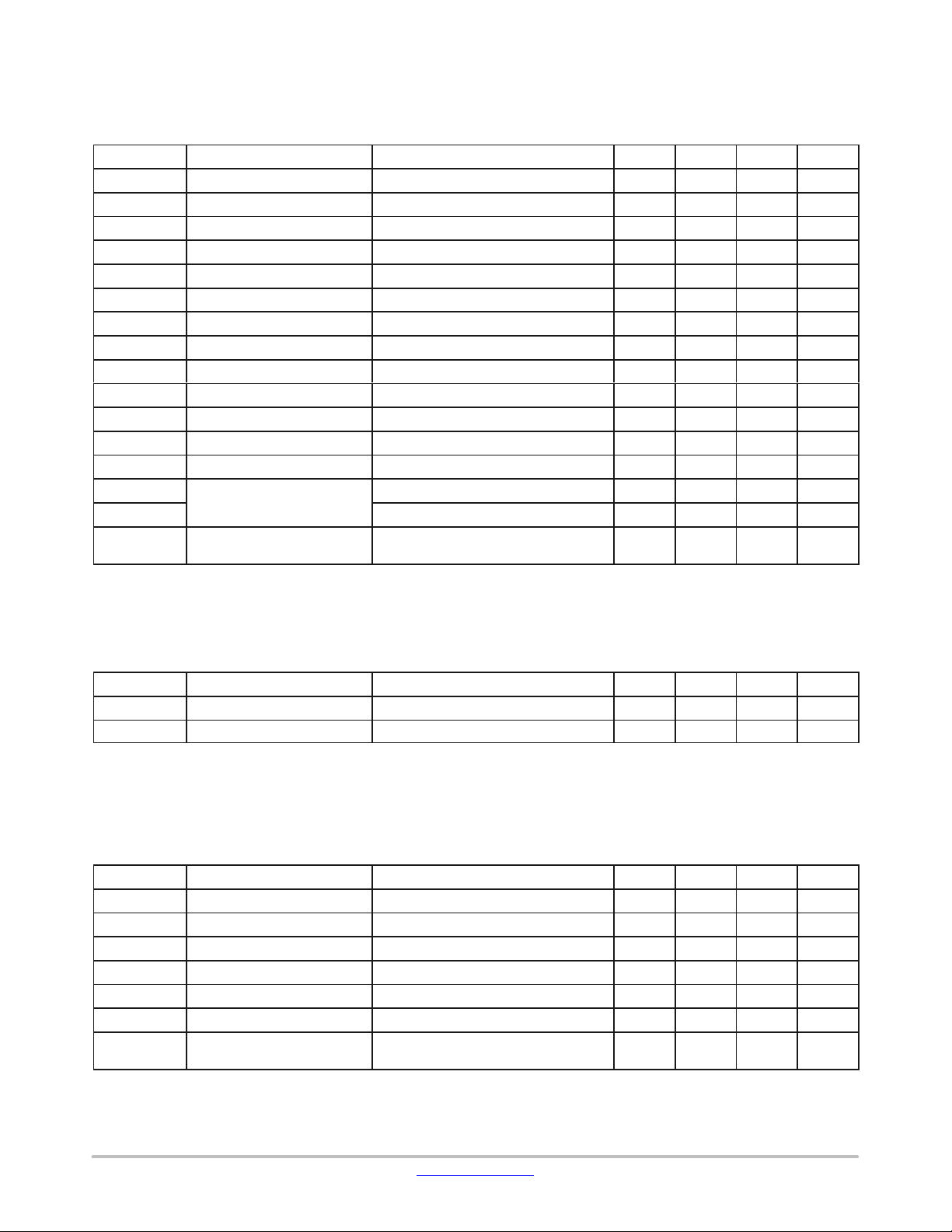
MAXIMUM RATINGS
MAXIMUM RATINGS
Symbol Parameter Conditions Min Typ Max Unit
VCC Supply Voltage
VCC_IN CC Voltage CC_IN to GND −0.5
VSW_USB USB Switch Voltage (DP_R, DN_L) to GND −3.5
VSW_SBU SBU Switch Voltage (SBUx, GSBUx) to GND −0.5
VSW_HOST Host Side Switch Voltage (DP, DN, S1H, S2H, SENSE, MIC) to GND −0.5
VSW_Audio Host Side Audio Switch Voltage (L, R) to GND −3.5
VCNTRL Control Pin Voltage (SDA, SCL, EN, DET, INT) to GND −0.5
IIK DC Input Diode Current −50
ISW_USB USB Switch Current Between DP_R and DP or DN_L and DN
ISW_SBU SBU Switch Current (S1H, S2H, MIC) to SBUx
ISW_SENSE Sense Switch Current GSBUx to SENSE
ISW_AGND Analog Ground Current SBUx to AGND
ISW_Audio Audio Switch Current DP_R to R or DN_L to L −250
ESDHBM
ESDHBM_Con Connector Side Pins and Power Pins 3.5
ESDCDM Charged Device Model,
Stresses exceeding those listed in the Maximum Ratings table may damage the device. If any of these limits are exceeded, device functionality
should not be assumed, damage may occur and reliability may be affected.
Human Body Model, JEDEC:
JS−001−2017
JEDEC: JS−002−2018
All Pins 2
−0.5 −
1
−
−
−
−
−
−
−
−
−
−
−
−
−
−
−
6.5 V
20 V
16 V
16 V
6.5 V
6.5 V
6.5 V
− mA
100 mA
50 mA
100 mA
500 mA
250 mA
− kV
− kV
kV
THERMAL PROPERTIES
THERMAL PROPERTIES
Symbol Parameter Conditions Min Typ Max Unit
T
STG
T
A
1. Junction−to−ambient thermal resistance is a function of application and board layout. This data is measured with two−layer 2s2p boards in
accordance to JEDEC standard JESD51. Special attention must be paid not to exceed junction temperature T
temperature T
Storage Temperature −65 150 °C
Operating Temperature −40 25 85 °C
at a given ambient
.
A
J(max)
OPERATING CONDITIONS
OPERATING CONDITIONS
Symbol Parameter Conditions Min Typ Max Unit
VCC Supply Voltage 2.7 − 5.5 V
VCC_IN CC Voltage CC_IN to GND 0 − 5.5 V
VSW_USB USB Switch Voltage (DP_R, DN_L, DP, DN) to GND 0 − 3.6 V
VSW_SBU SBU Switch Voltage (SBUx, GSBUx) to GND 0 − 3.6 V
VSW_HOST Host Side Switch Voltage (DP, DN, S1H, S2H, SENSE, MIC) to GND 0 − 3.6 V
VSW_Audio Host Side Audio Switch Voltage (DN_L, DP_R, L, R) to GND −3 − 3 V
VCNTRL
Functional operation above the stresses listed in the Recommended Operating Ranges is not implied. Extended exposure to stresses beyond
the Recommended Operating Ranges limits may affect device reliability.
Control Input Voltage
(EN, SCL1/SDA2, SDA1/SCL2)
VCC
www.onsemi.com
5
Page 6
FSA4485
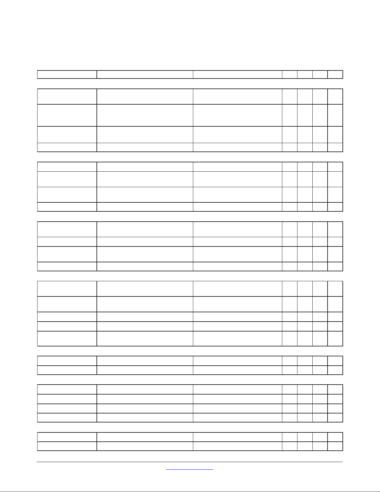
ELECTRICAL SPECIFICATION TABLE
ELECTRICAL SPECIFICATIONS
(Minimum and maximum values are at VCC = 2.7 V to 5.5 V and T
= 25°C, VCC = 3.3 V)
T
A
Symbol Parameter Conditions Min Typ Max Unit
CURRENT
ICC
ICC_AUDIO Audio Supply Current
ICCZ
ICCZ_H
USB/AUDIO COMMON PINS
IOZ
IOFF
VOV_TRIP Input OVP Lockout Rising Edge of DP_R, DN_L, SBUx,
VOV_HYS Input OVP Hysteresis DP_R, DN_L, SBUx, GSBUx − 0.3 − V
USB SWITCH
ION_USB
IOZ_USB USB Host Side Off Leakage Current DN, DP = 0 V to 3.6 V −3 3
IOFF_USB
RON_USB USB Switch On Resistance ISW = 8 mA, VSW = 0.4 V 3
AUDIO SWITCH
ION_AUDIO
IOFF_AUDIO
RON_AUDIO Audio Switch On Resistance
RON_FLAT
RSHUNT
SBU COMMON PINS
IOZ_SBU
IOFF_SBU
SBU DATA SWITCH
ION_SxH
IOZ_SxH Off Leakage Current (S1H, S2H) SxH =0 V to 3.6 V −1 1
IOFF_SxH
RON_SxH
MIC SWITCH
ION_MIC
IOZ_MIC Off Leakage Current (MIC) MIC = 0 V to 3.6 V −1 1
Supply Current
Quiescent Current, Software
Disabled
Quiescent Current, Hardware Disable
USB Connector Side Off Leakage Current
USB Connector Side Power Off Leakage
Current
USB Switch ON Leakage Current
USB Host Side Power Off Leakage
Current
ON Leakage Current of Audio Switch
Power Off Leakage Current of Audio
Switch L, R
Audio Switch On Resistance Flatness †
Pull Down Resistor on R/L Pin when Audio
Switch is Off
Off Leakage Current (SBU1, SBU2) SBUx = 0 V to 3.6 V −3 3
Power Off Leakage Current (SBU1, SBU2)
ON Leakage Current of SBU Switch SBUx = 0 V to 3.6 V, SxH = Float −3 3
Power Off Leakage Current (S1H, S2H)
SBU Switch On Resistance to (S1H, S2H)
ON Leakage Current of MIC Switch SBUx = 0 V to 3.6 V, MIC = Float −3 3
= −40°C to +85°C unless otherwise noted. Typical values are at
A
USB switches on, SBUx to SBUx_H
switches on
Audio switches closed, MIC switch
closed and
Audio GND switch closed
04H’b7 = 0, EN = Low or Float
EN = High 10
DP_R, DN_L = 0 V to 3.6 V −3 3
DP_R, DN_L = 0 V to 3.6 V, VCC = 0 V −3 3
GSBUx
DN_L, DP_R = 0 V to 3.6 V, DP, DN, R,
L = Float
DN, DP = 0 V to 3.6 V, VCC = 0 V −3 3
DN_L, DP_R = −3 V to 3.0 V, DP, DN,
R, L = Float
L, R = 0 V to 3 V; DP_R, DN_L = Float,
VCC = 0 V
ISW = 100 mA, VSW = −3 V to 3 V
VSW = −3.0 V to +3.0 V 10
L = R = 3 V 6 10 14
SBUx = 0 V to 3.6 V, VCC = 0 V −3 3
SxH =0 V to 3.6 V, VCC = 0 V −1 1
VSW = 0 V to 3.6 V, ISW = 20 mA 3
4.7 5 5.2 V
−3 3
−6 6
−1 1
65
A
65
A
5
A
A
A
A
A
A
A
A
A
1
m
k
A
A
A
A
A
A
A
www.onsemi.com
6
Page 7
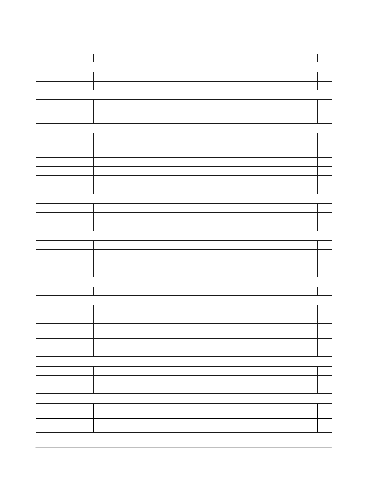
FSA4485
ELECTRICAL SPECIFICATIONS (continued)
(Minimum and maximum values are at VCC = 2.7 V to 5.5 V and T
T
= 25°C, VCC = 3.3 V)
A
MIC SWITCH
IOFF_MIC
RON_MIC SBU Switch On Resistance to (MIC) VSW = 0 V to 3.6 V, ISW = 20 mA 3
AGND SWITCH
RON_AGND
IOC_TRIP Input OCP Lockout SBUx to AGND 04h’b0 = 1, 07h = xx010xxxb or
SENSE SWITCH
ION_SENSE
IOZ_SENSE Off Leakage Current of SENSE Sense = 0 V to 1.0 V −3 3
IOZ_GSBU Off Leakage Current of GSBUx GSBUx = 0 V to 3.6 V −3 3
IOFF_SENSE
IOFF_GSBU
RON_SENSE Sense Switch On Resistance IOUT = 100 mA, VSW =1 V 250 400
CC_IN PIN
VTH_L_CC
VTH_H_CC Input High Threshold 1.5 V
IIN_CC CC_IN Input Leakage Current CC_IN = 0 V to 5.5 V 1
EN PIN
VIH_EN
VIL_EN EN Input Voltage Low 0.5 V
RFLOAT_EN Resistance from EN to GND 900
IIN_EN EN Input Leakage Current EN = 0 V to 5.5 V 10
DET & INT PIN
VOL
I2C PINS
VIL_I2C
VIH_I2C High Level Input Voltage 0.84 V
IIN_I2C Input Current SCL1/SDA2,
VOL_I2C Low Level Output Voltage IOL = 2 mA 0.3 V
VOH_I2C Low Level Output Current VOL_I2C = 0.2 V 10 mA
GATE DRIVE
I_GATE
V_GATE Gate Drive Voltage (GD1, GD2) † ILoad = 200 nA 6 V
R_GATE Gate Drive Discharge Resistance † 1.0
AUDIO SWITCH
tDELAY_Audio
tDELAY_Audio_Slow Audio Switch Turn On Delay with Slow
Power Off Leakage Current (MIC) MIC = 0 V to 3.6 V, VCC = 0 V −1 1
SBUx Switch On Resistance to AGND
ON Leakage Current of SENSE switch On GSBUx = 0 V to 1.0 V,
Power Off Leakage Current of SENSE
Power Off Leakage Current of GSBUx
Input Low Threshold 1.2 V
EN Input Voltage High 1.1 V
Output Low Voltage IOUT = 2 mA 0.4 V
Low Level Input Voltage 0.36 V
Gate Drive Current (GD1, GD2) † V_GATE = 3 V 2
Audio Switch Turn On Delay Time †
Turn On †
= −40°C to +85°C unless otherwise noted. Typical values are at
A
ISW = 100 mA on SBUx 78 125
xxxxx010b
Off GSBUx = 2 V, Sense = Float
Sense = 0 V to 1.0 V, VCC = 0 V −3 3
GSBUx = 0 V to 3.6 V, VCC = 0 V −3 3
SDA1/SCL2 = 0 V to 3.6 V
DP_R = DN_L = 1 V, RL = 32 ,
SLOW_TURN_ON = 0b
DP_R = DN_L = 1 V, RL = 32 ,
SLOW_TURN_ON = 1b
0.75 1.5 3.0 A
−2 2
−2 2
100
150
UnitMaxTypMinConditionsParameterSymbol
A
m
A
A
A
A
A
m
A
K
A
A
A
M
s
s
www.onsemi.com
7
Page 8
FSA4485
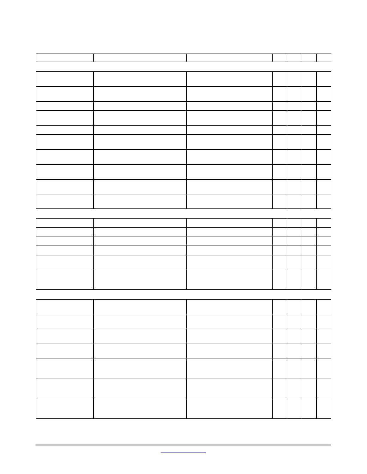
ELECTRICAL SPECIFICATIONS (continued)
(Minimum and maximum values are at VCC = 2.7 V to 5.5 V and T
T
= 25°C, VCC = 3.3 V)
A
AUDIO SWITCH
tRISE_Audio
tRISE_Audio_Slow Audio Switch Turn On Rise Time with Slow
tOFF_Audio Audio Switch Turn Off Time †
XTALK_Audio Crosstalk between Left and Right †
BW_Audio −3dB Bandwidth †
OIRR_Audio Off Isolation †
THD+N_600 Total Harmonic Distortion + Noise
THD+N_32 Total Harmonic Distortion + Noise
THD+N_16 Total Harmonic Distortion + Noise
PSRR_Audio Power Supply Rejection Ratio to Audio † Supply Noise = 300mVpp, f = 217 Hz,
USB SWITCH
tON_USB
tOFF_USB
BW_USB
IL_USB Insetrion Loss †
OIRR_USB
tOVP_USB
MIC/AUDIO GROUND SWITCH
tDELAY_MIC
tDELAY_MIC_Slow MIC Switch Turn On Delay with Slow Turn
tRISE_MIC MIC Switch Turn On Rising Time with Slow
tRISE_MIC_Slow MIC Switch Turn On Rising Time with Slow
tDELAY_AGND AGND Switch Turn On Time with Slow
tDELAY_AGND_Slow AGND Switch Turn On Time with Slow
tRISE_AGND AGND Switch Turn On Rise Time with
Audio Switch Turn On Rise Time †
Turn On †
Performance with A−weighting Filter †
Performance with A−weighting Filter †
Performance with A−weighting Filter †
USB Switch Turn−on Time † DP_R = DN_L = 1.5 V, RL = 50
USB Switch Turn −off Time † DP_R = DN_L = 1.5 V, RL = 50
−3 dB Differential Bandwidth † RL = 50
Off Isolation between DP, DN and
Common Node Pins †
DP_R and DN_L pins OVP Response
Time †
MIC Switch Turn On Delay Time with Slow
Turn On Disabled †
On Enabled †
Turn On Disabled †
Turn On Enabled †
Turn On Disabled †
Turn On Enabled †
Slow Turn On Disabled †
= −40°C to +85°C unless otherwise noted. Typical values are at
A
DP_R = DN_L = 1 V, RL = 32 ,
SLOW_TURN_ON = 0b
DP_R = DN_L = 1 V, RL = 32 ,
SLOW_TURN_ON = 1b
DP_R = DN_L = 1 V, RL = 32
f = 1 kHz, RL = 50 to GND,
VSW = 1 VRMS
VSW = 200 mV, RL = 50
F = 1 kHz, RL = 50 , CL = 0 pF,
VSW = 1 VRMS
RL = 600 , f = 20 Hz~20 kHz,
VSW = 2 VRMS
RL = 32 , f = 20 Hz~20 kHz,
VSW = 1 VRMS
RL = 16 , f = 20 Hz~20 kHz,
VSW = 0.5 VRMS
RL = 50 , Audio Switch Closed
RL = 50 , f = 720 MHz
f = 1 kHz, RL = 50 , CL = 0 pF,
VSW = 1 VRMS
Rising edge of DP_R or DN_L ≥ 4.8 V
to falling edge of DP or DN or L or
R ≤ 4.8 V, RL on DP or DN = 1 k
SBUx = 1 V, RL = 50 ,
SLOW_TURN_ON = 0b
SBUx = 1 V, RL = 50 ,
SLOW_TURN_ON = 1b
SBUx = 1 V, RL = 50 ,
SLOW_TURN_ON = 0b
SBUx = 1 V, RL = 50 ,
SLOW_TURN_ON = 1b
SBUx pulled up to 0.5 V by 16 ,
AGND connect to GND,
SLOW_TURN_ON = 0b
SBUx pulled up to 0.5 V by 16 ,
AGND connect to GND,
SLOW_TURN_ON = 1b
SBUx pulled up to 0.5 V by 16 ,
AGND connect to GND,
SLOW−TURN_ON = 0b
UnitMaxTypMinConditionsParameterSymbol
26
180
15
−100 dB
550 MHz
−100 dB
−100 dB
−109 dB
−108 dB
−70 dB
33
15
1 GHz
−2.2 dB
-100
600 ns
90
200
40
300
660
1100
270
s
s
s
s
s
dB
s
s
s
s
s
s
s
www.onsemi.com
8
Page 9
FSA4485
ELECTRICAL SPECIFICATIONS (continued)
(Minimum and maximum values are at VCC = 2.7 V to 5.5 V and T
T
= 25°C, VCC = 3.3 V)
A
MIC/AUDIO GROUND SWITCH
tRISE_AGND_Slow
tOFF_MIC MIC Switch Turn Off Time †
tOFF_AGND AGND Switch Turn Off Time † SBUx: Vsource = 2.5 V,
BW MIC Switch Bandwidth †
tOC_DEB SBUx to AGND Over Current Debounce
SBU SWITCH
tON_SBU
tOFF_SBU SBUx_H Switch Turn Off Time †
BW_SBU Bandwidth †
tOVP_SBU SBUx Pins OVP Response Time †
SENSE SWITCH
tDELAY_SENSE
tDELAY_SENSE_Slow Sense Switch Turn On Delay with Slow
tRISE_SENSE Sense Switch Turn On Rise Time with
tRISE_SENSE_Slow Sense Switch Turn On Rise Time with
tOFF_SENSE Sense Switch Turn Off Time †
tOVP_SENSE GSBUx Pins OVP Response Time † Rising edge of GSBUx ≥ 4.8 V to
BW_SENSE Bandwidth †
DET DELAY
tDELAY_DET
I2C SPECIFICATIONS
fSCL
tHD; STA
tLOW Low Period of I2C_SCL Clock † 1.3
tHIGH High Period of I2C_SCL Clock † 0.6
tSU; STA
tHD; DAT Data Hold Time † 0 0.9
tSU; DAT
tr
tf
tSU; STO
AGND Switch Turn On Rise Time with
Slow Turn On Enabled †
Time †
SBUx_H Switch Turn On Time †
Sense Switch Turn On Delay with Slow
Turn On Disabled †
Turn On Enabled †
Slow Turn On Disabled †
Slow Turn On Enabled †
DET Response Delay † Transition from High−Z to 0 V 2.5
I2C_SCL Clock Frequency 400 kHz
Hold Time (Repeated) START Condition †
Set−up Time for Repeated START
Condition †
Data Set−up Time †
Rise Time of I2C_SDA and I2C_SCL
Signals †
Fall Time of I2C_SDA and I2C_SCL
Signals †
Set−up Time for STOP Condition †
= −40°C to +85°C unless otherwise noted. Typical values are at
A
SBUx pulled up to 0.5 V by 16 ,
AGND connect to GND,
SLOW−TURN_ON = 1b
SBUx = 2.5 V, RL = 50
clamp to 10 mA
RL = 50
SBUx = 2.5 V, RL = 50
SBUx = 2.5 V, RL = 50
RL = 50
Rising edge of SBUx ≥ 4.8 V to falling
edge of SxH ≤ 4.8 V, RL on SxH = 1 k
GSBUx = 1 V, RL = 50 ,
SLOW_TURN_ON = 0b
GSBUx = 1 V, RL = 50 ,
SLOW_TURN_ON = 1b
GSBUx = 1 V, RL = 50 ,
SLOW_TURN_ON = 0b
GSBUx = 1 V, RL = 50 ,
SLOW_TURN_ON = 1b
GSBUx = 1 V, RL = 50
falling edge of SENSE ≤ 4.8 V, RL on
SENSE = 1 k
RL = 50
0.1Cb
0.1Cb
UnitMaxTypMinConditionsParameterSymbol
720
15
15
35 MHz
500
75
15
35 MHz
250 ns
150
110
110
110
15
250 ns
108 MHz
0.6
0.6
100 ns
20 +
20 +
0.6
300 ns
300 sn
s
s
s
s
s
s
s
s
s
s
s
s
s
s
s
s
s
s
www.onsemi.com
9
Page 10

FSA4485
ELECTRICAL SPECIFICATIONS (continued)
(Minimum and maximum values are at VCC = 2.7 V to 5.5 V and T
T
= 25°C, VCC = 3.3 V)
A
I2C SPECIFICATIONS
tBUF
tSP
CAPACITANCE
CON_USB
COFF_ USB
COFF_USBHost Off Capacitance of USB Host Pins †
CON_SENSE On Capacitance of GSBUx †
COFF_SENSE Off Capacitance of GSBUx †
CON_MIC
COFF_MIC Off Capacitance of MIC †
CON_AGND
CON_SBU
COFF_SBU Off Capacitance of SBUx †
COFF_SBUHost
CCNTRL Control Input Pin Capacitance †
Product parametric performance is indicated in the Electrical Characteristics for the listed test conditions, unless otherwise noted. Product
performance may not be indicated by the Electrical Characteristics if operated under different conditions.
Guarantee Levels:
†Guaranteed by Design. Characterized on the ATE or Bench.
Bus−Free Time between STOP and
START Conditions †
Pulse Width of Spikes that Must Be
Suppressed by the Input Filter †
On Capacitance of USB Common Pins †
Off Capacitance of USB Common Pins †
On Capacitance of SBUx to MIC Switch †
On Capacitance of SBUx to AGND
Switch †
On Capacitance of SBUx to SxH Switch †
On Capacitance of SBUx to SxH Switch †
= −40°C to +85°C unless otherwise noted. Typical values are at
A
1.3
0
f = 1 MHz, 100 mVPK−PK, 100 mV DC
f = 1 MHz, 100 mVPK−PK, 100 mV DC
f = 1 MHz, 100 mVPK−PK, 100 mV DC
f = 1 MHz, 100 mVPK−PK, 100 mV DC
f = 1 MHz, 100 mVPK−PK, 100 mV DC
f = 1 MHz, 100 mVPK−PK, 100 mV DC
f = 1 MHz, 100 mVPK−PK, 100 mV DC
f = 1 MHz, 100 mVPK−PK, 100 mV DC
f = 1 MHz, 100 mVPK−PK, 100 mV DC
f = 1 MHz, 100 mVPK−PK, 100 mV DC
f = 1 MHz, 100 mVPK−PK, 100 mV DC
f = 1 MHz, 100 mVPK−PK, 100 mV DC
50 ns
8.5 pF
9.5 pF
3.0 pF
34 pF
44 pF
115 pF
8.5 pF
94.5 pF
114 pF
108 pF
9.0 pF
5.0 pF
UnitMaxTypMinConditionsParameterSymbol
s
www.onsemi.com
10
Page 11

FSA4485
FUNCTIONAL SPECIFICATIONS
I2C Interface
The FSA4485 includes a full I2C slave controller. The I2C
slave fully complies with the I
2
C specification version 2.1
requirements. This block is designed for fast mode, 400 kHz,
2
signals. Examples of an I
C write and read sequence are
shown in below figures respectively.
Table 2. I2C SLAVE ADDRESS
SDA SCL Bit 7 Bit 6 Bit 5 Bit 4 Bit 3 Bit 2 Bit 1 Bit 0
SDA1 SCL1 1 0 0 0 0 1 0 R/W
SDA2 SCL2 1 0 0 0 0 1 1 R/W
Figure 3. I2C Write Example
The I2C Address can be selected by routing the SDA/SCL
signals per the Table 2 below. The FSA4485 will detect the
clock and automatically configure the I/O and address. The
I2C interface will operate with VDDIO pull up from 1.2 V
to 1.8 V.
Figure 4. I2C Read Example
Over Voltage Protection
FSA4485 features over voltage protection (OVP) on the
receptacle side pins. This will automatically switch open the
internal signal routing path if the input voltage exceeds the
OVP threshold. If OVP has occurred an interrupt signal will
be send using the INT signal. The OVP_INTERRUPT
register will indicate which pin had the OVP event. If the
over voltage is no longer present, indicated by the
OVP_STAT register, the signal path can be restored
manually from the SWITCH_SEL register.
Over Current Protection
When the EN_OCP register is set to Enable and the SBUx
switch is closed to AGND Over Current Protection (OCP)
will be enabled. OCP monitors the voltage drop from SBUx
to AGND across the closed switch to limit the current to
1.5 A for 500 s. This will prevent a short from VBUS to
AGND through SBUx. OCP will not automatically reset.
When an OCP event occurs an interrupt will be sent to the
processor. The interrupt is cleared by reading the
www.onsemi.com
I_OCP_AGND register. The SBUx to AGND switch can be
closed after an OCP event by setting AGND_EN = 1b.
MIC Switch Auto−Off
MIC switch auto−off is controlled by the
MIC_AUTO_OFF register (12h, Bit 2). If enabled, when the
port is configured for audio (L, R, MIC, AGND switches are
closed) and a detach is detected (CC_IN > 1.5 V) the
receptacle side of the MIC switch will connect to ground for
50 s prior to becoming high impedance.
Headset Detection
Headset detection is performed by the CC_IN input and
indicated by the CC_IN_STAT register (11h, Bit 2). Headset
detection can also be indicated by the DET output. DET is
an Open Drain user configurable attach/detach detection
output. It can be configured or disabled from the I
2
DET_FUNCT. The DET output once triggered can be
cleared by reading the Detection Interrupt Register
I_DET_FUNCT. When configured for Type−C or Audio
11
C register
Page 12

FSA4485
Accessory attach detection DET will clear automatically
when the Type−C device or audio accessory is detached.
Figure 5. Detect Pin Function
Gate Drive
The FSA4485 includes two gate drive outputs GD1 and
GD2 to allow a low resistance external switch to be used for
AGND. The gate drives are enabled from the I
2
C register
GATE_DRIVE_EN and will follow automatic orientation
detection. When enabled, if SBU1 = AGND then GD1 =
High, If SBU2 = AGND then GD2 = High.
GATE DRIVE CURRENT
Register Value GATE_DRIVE_CURR
00b
01b
10b
11b
EN and Factory Mode
The enable input (EN) is a 3 state input which sets the USB
and SBU data switch initial conditions during device power
up. It has a weak internal pull down which will set the default
condition to High−Z if no input level is present. For
applications using the SBU signals for data the EN input can
The gate to source voltage (Vgs) will be held at V_GATE
to ensure low on resistance. The maximum gate drive
current can be selected from the I
2
C register
GATE_DRIVE_CURR to control switch turn on time.
1 A
1.5 A
2.0 A (default)
3.0 A
be floated or connected to a GPIO in High−Z state at power
up. For typical conditions EN can be tied to GND. EN is tied
to GND using a 10 k resistor if also using the EN input to
disable the device. It is not recommended that the EN =
High−Z condition be used if the system uses SBU for the
DisplayPort Aux channel.
Figure 6. EN Input Truth Table
www.onsemi.com
12
Page 13

FSA4485
Moisture Detection
The moisture detection function is controlled the
RES_DETECT register (12h, Bit 1). It will detect moisture
or any foreign object that creates resistance between the
receptacle side pins and ground. During resistance
detection, the switch associated with the pin will be open.
The detection result will be saved in the RES_VALUE
register (14h). The measurement range is from 1 k to
2.56 M and is controlled by the RES_DET_RANGE
register (12h, Bit 5). Detection can be performed manually
or an automatic detection interval can be set to 100 ms, 1 s
or 10 s by the RED_DET_INTV register (16h).
Test Diagrams
Figure 9. On Resistance
Figure 7. Moisture Detection Procedure
Figure 8. Off Leakage (IOZ)
www.onsemi.com
13
Page 14

FSA4485
Figure 10. On Leakage Figure 11. Power Off Leakage (IOFF)
Figure 12. Test Circuit Load Figure 13. Manual Mode Turn On/Off Waveform
Figure 14. Bandwidth Figure 15. Channel Off Isolation
www.onsemi.com
14
Page 15

FSA4485
Figure 16. Adjacent Channel Crosstalk Figure 17. Channel Off Capacitance
Figure 18. Channel Off Capacitance
Figure 19. Total Harmonic Distortion (THD + N)
www.onsemi.com
15
Page 16

FSA4485
REGISTER MAPPING TABLE
REGISTER MAPPING
Read Only Write Only Read / Write Read / Clear Write / Clear
Address Name Bit[7] Bit[6] Bit[5] Bit[4] Bit[3] Bit[2] Bit[1] Bit[0]
0x00 DEVID VENID VERID REVID
0x01 OVP_MASK M_OCP_AGND M_OVP_ALL M_OVP_DP_R M_OVP_DN_L M_OVP_SBU1 M_OVP_SBU2 M_OVP_GSBU1 M_OVP_GSBU2
0x02 OVP_INTERRUPT I_OCP_AGND I_OVP_ALL I_OVP_DP_R I_OVP_DN_L I_OVP_SBU1 I_OVP_SBU2 I_OVP_GSBU1 I_OVP_GSBU2
0x03 OVP_STAT Reserved OCP_STAT
0x04 SWITCH_EN DEVICE_EN S1H_EN S2H_EN DN_L_EN DP_R_EN SENSE_EN MIC_EN AGND_EN
0x05 SWITCH_SEL Reserved S1H_SEL S2H_SEL DN_L_SEL DP_R_SEL SENSE_SEL MIC_SEL AGND_SEL
0x06 SWITCH_STAT_1 Reserved SENSE_STAT DP_R_STAT DN_L_STAT
0x07 SWITCH_STAT_2 Reserved SBU2_STAT SBU1_STAT
0x08 AUDIO_SLO W_LEFT AUDIO_SLOW_LEFT
0x09 AUDIO_SLO W_RIGHT AUDIO_SLOW_RIGHT
0x0A MIC_SLOW MIC_SLOW
0x0B SENSE_SLOW SENSE_SLOW
0x0C AGND_SLOW AGND_SLOW
0x0D L2R_EN_DELAY L2R_EN_DELAY
0x0E MIC2L_EN_ DELAY MIC2L_EN
0x0F SENSE2L_EN_DELAY SENSE2L_EN_DELAY
0x10 AGND2L_EN_DELAY AGND2L_EN_DELAY
0x11 AUDIO_ACC_STAT Reserved CC_IN_STAT DET_STAT
0x12 FUNCTION_ EN DET_FUNCT RES_DET
0x13 RES_PIN_SEL Reserved RES_PIN_SEL
0x14 RES_VALUE RES_VALUE
0x15 RES_DET_THRESH RES_DET_THRESH
0x16 RES_DET_INTV Reserved RES_DET_INTV
0x17 AUDIO_JACK_STAT Reserved UNKNOWN
0x18 DET_INTERRUPT Reserved I_DISABLE I_DET_FUNCT I_AUDIO_JACK
0x19 DET_MASK Reserved M_DISABLE M_DET M_AUDIO
0x1A AUDIO_JACK_DET1 AUDIO_JACK_DET1
0x1B AUDIO_JACK_DET2 AUDIO_JACK_DET2
0x1C MIC_DET_TH_LOW MIC_DET_TH_LOW
0x1D MIC_DET_TH_UP MIC_DET_TH_UP
0x1E I2C_RESET Reserved I2C_RESET
0x1F CURR_SOURCE_SET Reserved CURR_SOURCE_SET
0x20 CURR_SOURCE_STAT Reserved CURR_SOURCE_STAT
0x21 GATE_DRIVE Reserved GATE_DRIVE
0x22 PROTECTION_EN Reserved EN_OVP EN_OCP
0x23 PROTECTION_STAT Reserved USB_OVP GSBU_OVP SBU1_OVP SBU2_OVP OCP1 OCP2
_AGND
OVP_STAT
_DP_R
_RANGE
OVP_STAT
_DN_L
HIZ_ACC_DET SLOW_TURN
_AUDIO_ACC
OVP_STAT
_SBU1
_DELAY
_ON
4POLE_A 4POLE_B 3POLE NO_AUDIO_ACC
OVP_STAT
_SBU2
MIC_AUT_OFF RES_DETECT AUDIO_JACK
_DET
_JACK_DET
_EN
OVP_STAT
_GSBU1
I_LOW_RES I_RES_DET
M_LOW_RES M_RES
GATE_DRIVE_CURR
OVP_STAT
_GSBU2
_COMP
_DET
www.onsemi.com
16
Page 17

FSA4485
REGISTER DETAILS
Table 3. DEVICE ID
0x00 DEVID
Bit Name Default Type Description
7:6 VENID 00 Read Vendor ID
5:3 VERID 001 Read
2:0 REVID 001 Read
Revision ID Low: 001h
A_[Revision ID]: 0x001 (e.g. A_revA)
B_[Revision ID]: 0x010 (e.g. B_revA)
C_[Revision ID]: 0x011 (e.g. C_revA) etc
Revision ID Low: 001h
A_[Revision ID]: 0x001 (e.g. A_revA)
B_[Revision ID]: 0x010 (e.g. A_revB)
C_[Revision ID]: 0x011 (e.g. A_revC) etc
Table 4. OVP/OCP INTERRUPT MASK
0x01 OVP_MASK
Bit Name Default Type Description
7 M_OCP_AGND 0 R/W
6 M_OVP_ALL 0 R/W
5 M_OVP_DP_R 0 R/W
4 M_OVP_DN_L 0 R/W
3 M_OVP_SBU1 0 R/W
2 M_OVP_SBU2 0 R/W
1 M_OVP_GSBU1 0 R/W
0 M_OVP_GSBU2 0 R/W
0b: Do not mask OCP interrupt
1b: Mask OCP interrupt on SBUx to AGND
0b: OCP Mask is controled by bit 7, OVP Mask is controled by bit [5:0]
1b: Mask OVP/OCP interrupt on all connector side pins
0b: Do not mask OVP interrupt
1b: Mask OVP interrupt on DP_R
0b: Do not mask OVP interrupt
1b: Mask OVP interrupt on DN_L
0b: Do not mask OVP interrupt
1b: Mask OVP interrupt on SBU1
0b: Do not mask OVP interrupt
1b: Mask OVP interrupt on SBU2
0b: Do not mask OVP interrupt
1b: Mask OVP interrupt on GSBU1
0b: Do not mask OVP interrupt
1b: Mask OVP interrupt on GSBU2
Default = 00001001
Default = 00000000
www.onsemi.com
17
Page 18

FSA4485
Table 5. OVP/OCP INTERRUPT FLAG
0x02 OVP_INTERRUPT
Bit Name Default Type Description
7 I_OCP_AGND 0 R/CLR
6 I_OVP_ALL 0 R/CLR
5 I_OVP_DP_R 0 R/CLR
4 I_OVP_DN_L 0 R/CLR
3 I_OVP_SBU1 0 R/CLR
2 I_OVP_SBU2 0 R/CLR
1 I_OVP_GSBU1 0 R/CLR
0 I_OVP_GSBU2 0 R/CLR
0b: OCP has not occured
1b: OCP event has occured on SBUx to AGND
0b: OVP or OCP event has not occurred
1b: OVP or OCP event has occurred
0b: OVP event has not occured
1b: OVP event has occurred on DP_R
0b: OVP event has not occured
1b: OVP event has occurred on DN_L
0b: OVP event has not occured
1b: OVP event has occurred on SBU1
0b: OVP event has not occured
1b: OVP event has occurred on SBU2
0b: OVP event has not occured
1b: OVP event has occurred on GSBU1
0b: OVP event has not occured
1b: OVP event has occurred on GSBU2
Default = 00000000
Table 6. OVP/OCP STATUS
0x03 OVP_STAT
Bit Name Default Type Description
7 Reserved 0 Read Do Not Use
6 OCP_STAT_AGND 0 Read
5 OVP_STAT_DP_R 0 Read
4 OVP_STAT_DN_L 0 Read
3 OVP_STAT_SBU1 0 Read
2 OVP_STAT_SBU2 0 Read
1 OVP_STAT_GSBU1 0 Read
0 OVP_STAT_GSBU2 0 Read
0b: OCP event has not occured
1b: OCP event has occurred on SBUx to AGND
0b: OVP event has not occured
1b: OVP event has occurred on DP R
0b: OVP event has not occured
1b: OVP event has occurred on DN L
0b: OVP event has not occured
1b: OVP event has occurred on SBU1
0b: OVP event has not occured
1b: OVP event has occurred on SBU2
0b: OVP event has not occured
1b: OVP event has occurred on GSBU1
0b: OVP event has not occured
1b: OVP event has occurred on GSBU2
Default = 00000000
www.onsemi.com
18
Page 19

FSA4485
Table 7. SWITCH ENABLE
0x04 SWITCH_EN
Bit Name Default Type Description
7 DEVICE_EN 1 R/W
6 S1H_EN 0 R/W
5 S2H_EN 0 R/W
4 DN_L_EN 1 R/W
3 DP_R_EN 1 R/W
2 SENSE_EN 0 R/W
1 MIC_EN 0 R/W
0 AGND_EN 0 R/W
0b: Device Disabled, L and R = 10 k Pull Down, All Other Switches = High−Z,
this overrides EN = Low
1b: Device Enabled, All Switches are Enabled, this can be overridden by EN = High
0b: Switch Disabled, S1H = High−Z
1b: SBUx to S1H Switch Enabled
0b: Switch Disabled, S2H = High−Z
1b: SBUx to S2H Switch Enabled
0b: Switch Disabled, DN = High−Z, L = 10 k Pull Down
1b: DN L Switch Enabled
0b: Switch Disabled, DP = High−Z, R = 10 k Pull Down
1b: DP R Switch Enabled
0b: Switch Disabled, SENSE, GSBU1 and GSBU2 = High−Z
1b: SENSE Switch Enabled
0b: Switch Disabled, MIC = High−Z
1b: MIC to SBUx Switch Enabled
If S1H EN and/or S2H EN = 1b then MIC will = High−Z when MIC EN = 1b
0b: Switch Disabled, AGND = High−Z
1b: AGND to SBUx Switch Enabled
If S1H EN and/or S2H EN = 1b then AGND will = High−Z when AGND EN = 1b
Default = 10011000
Table 8. SWITCH SELECT
0x05 SWITCH_SEL
Bit Name Default Type Description
7 Reserved 0 R/W Do Not Use
6 S1H_SEL 0 R/W
5 S2H_SEL 0 R/W
4 DN_L_SEL 1 R/W
3 DP_R_SEL 1 R/W
2 SENSE_SEL 0 R/W
1 MIC_SEL 0 R/W
0 AGND_SEL 0 R/W
0b: S1H to SBU1 switch is CLOSED
1b: S1H to SBU2 switch is CLOSED
0b: S2H to SBU2 switch is CLOSED
1b: S2H to SBU1 switch is CLOSED
0b: DN_L to L switch is CLOSED
1b: DN L to DN switch is CLOSED
0b: DP_R to R switch is CLOSED
1b: DP R to DP switch is CLOSED
0b: SENSE to GSBU1 switch is CLOSED
1b: SENSE to GSBU2 switch is CLOSED
0b: MIC to SBU2 switch is CLOSED
1b: MIC to SBU1 switch is CLOSED
If AGND_SEL = 0b and MIC_SEL = 1b when AGND_EN and MIC_EN = 1b then
MIC = High−Z If AGND SEL = 1b and MIC SEL = 0b when AGND EN and
MIC EN = 1b then MIC = High−Z
0b: AGND to SBU1 switch is CLOSED
1b: AGND to SBU2 switch is CLOSED
Default = 00011000
www.onsemi.com
19
Page 20

FSA4485
Table 9. SWITCH STATUS 1
0x06 SWITCH_STAT_1
Bit Name Default Type Description
7:6 Reserved 00 Read Do Not Use
5:4 SENSE_STAT 00 Read
3:2 DP_R_STAT 00 Read
1:0 DN_L_STAT 00 Read
00b: SENSE switch is OPEN
01b: SENSE switch is CLOSED to GSBU1
10b: SENSE Switch is CLOSED to GSBU2
11b: Not Valid
00b: DP_R switch is OPEN
01b: DP_R switch is CLOSED to DP
10b: DP_R Switch is CLOSED to R
11b: Not Valid
00b: DN_L switch is OPEN
01b: DN_L switch is CLOSED to DN
10b: DN_L Switch is CLOSED to L
11b: Not Valid
Table 10. SWITCH STATUS 2
0x07 SWITCH_STAT_2
Bit Name Default Type Description
7:6 Reserved 00 Read Do Not Use
5:3 SBU2_STAT 000 Read 000b: SBU2 switch is OPEN
001b: SBU2 switch is CLOSED to MIC
010b: SBU2 Switch is CLOSED to AGND
011b: SBU2 Switch is CLOSED to S1H
100b: SBU2 Switch is CLOSED to S2H
101b: SBU2 Switch is CLOSED to both S1H and S2H
110b: Not Valid
111b: Not Valid
2:0 SBU1_STAT 000 Read 000b: SBU1 switch is OPEN
001b: SBU1 switch is CLOSED to MIC
010b: SBU1 Switch is CLOSED to AGND
011b: SBU1 Switch is CLOSED to S1H
100b: SBU1 Switch is CLOSED to S2H
101b: SBU1 Switch is CLOSED to both S1H and S2H
110b: Not Valid
111b: Not Valid
Default = 00000000
Default = 00000000
Table 11. AUDIO SWITCH LEFT CHANNEL SLOW TURN ON TIME
0x08 AUDIO_SLOW_LEFT
Bit Name Default Type Description
7:0 AUDIO_SLOW_LEFT 00000001 R/W
00000000b: = 180 s
00000001b: = 330 s (DEFAULT)
Typical turn on time (tON) is incremented approximately 150 s per bit
Default = 00000001
Table 12. AUDIO SWITCH RIGHT CHANNEL SLOW TURN ON TIME
0x09 AUDIO_SLOW_RIGHT
Bit Name Default Type Description
7:0 AUDIO_SLOW_RIGHT 00000001 R/W
00000000b: = 180 s
00000001b: = 330 s (DEFAULT)
Typical turn on time (tON) is incremented approximately 150 s per bit
Default = 00000001
www.onsemi.com
20
Page 21

FSA4485
Table 13. MIC SWITCH SLOW TURN ON TIME
0x0A MIC_SLOW
Bit Name Default Type Description
7:0 MIC_SLOW 00000010 R/W 00000000b: = Do Not Use
00000001b: = 370 s
00000010b: = 520 s (DEFAULT)
Typical turn on time (tON) is incremented approximately 150 s per bit
Table 14. SENSE SWITCH SLOW TURN ON TIME
0x0B SENSE_SLOW
Bit Name Default Type Description
7:0 SENSE_SLOW 00000001 R/W
00000000b: = 160 s
00000001b: = 220 s (DEFAULT)
Typical turn on time (tON) is incremented approximately 60 s per bit
Table 15. AGND SWITCH SLOW TURN ON TIME
0x0C AGND_SLOW
Bit Name Default Type Description
7:0 AGND_SLOW 00000001 R/W
00000000b: = 900 s
00000001b: = 1750 s (DEFAULT)
Default = 00000010
Default = 00000001
Default = 00000001
Typical turn on time (tON) is incremented approximately 850 s per bit
Table 16. TIMING DELAY BETWEEN AUDIO L AND AUDIO R SWITCH ENABLE
0x0D L2R_EN_DELAY
Bit Name Default Type Description
7:0 L2R_EN_DELAY 00000000 R/W
00000000b: = 0 s (DEFAULT)
00000001b: = 100 s
……..
11111111b: = 25500 s
Increment size is 100 s per bit
Default = 00000000
Table 17. TIMING DELAY BETWEEN AUDIO MIC AND AUDIO L SWITCH ENABLE
0x0E MIC2L_EN_DELAY
Bit Name Default Type Description
7:0 MIC2L_EN_DELAY 00000000 R/W
00000000b: = 0 s (DEFAULT)
00000001b: = 100 s
……..
11111111b: = 25500 s
Increment size is 100 us per bit
Default = 00000000
www.onsemi.com
21
Page 22

FSA4485
Table 18. TIMING DELAY BETWEEN SENSE SWITCH AND AUDIO L SWITCH ENABLE
0x0F SENSE2L_EN_DELAY
Bit Name Default Type Description
7:0 SENSE2L_EN_DELAY 00000000 R/W
00000000b: = 0 s (DEFAULT)
00000001b: = 100 s
……..
11111111b: = 25500 s
Increment size is 100 s per bit
Table 19. TIMING DELAY BETWEEN AGND SWITCH AND AUDIO L SWITCH ENABLE
0x10 AGND2L_EN_DELAY
Bit Name Default Type Description
7:0 AGND2L_EN_DELAY 00000000 R/W
00000000b: = 0 s (DEFAULT)
00000001b: = 100 s
……..
11111111b: = 25500 s
Increment size is 100 s per bit
Table 20. AUDIO ACCESSORY STATUS
0x11 AUDIO_ACC_STAT
Bit Name Default Type Description
7:2 Reserved 000000 Read Reserved
1 CC_IN_STAT 1 Read
0 DET_STAT 1 Read
0b: CC_IN < V_TH_L_CC
1b: CC_IN > V_TH_H_CC
0b: DET output is LOW
1b: DET output is High−Z
Default = 00000000
Default = 00000000
Default = 00000011
www.onsemi.com
22
Page 23

FSA4485
Table 21. AUTOMATIC FUNCTION ENABLE
0x12 FUNCTION_EN
Bit Name Default Type Description
7:6 DET_FUNCT 11 R/W DET Output Configuration
00b: Type−C Attach Detection, DET = LOW if CC_IN_STAT = 0b
01b: Audio Accessory Attach Detection, DET = LOW if NO_AUDIO_ACC = 0b
10b: Audio Accessory Detach Detection, DET = LOW if CC_IN_STAT transitions
from 0b to 1b
11b: Disabled, DET = High−Z (DEFAULT)
5 RES_DET_RANGE 0 R/W
4 HIZ_ACC_DET 0 R/W
3 SLOW_TURN_ON 1 R/W
2 MIC_AUTO_OFF 0 R/W
1 RES_DETECT 0 R/W
0 AUDIO_JACK_DET 0 R/W
Resistor Detection Range Setting
0b: 1 k to 256 k
1b: 10 k to 2560 k
High Impedance Audio Accessory Detection
0b: Automatic Hi−Z Accessory Detection is disabled
1b: Automatic Hi−Z Accessory Detection is enabled
Switch Slow Turn On Control Enable
0b: Disabled 1b: Enabled
0b: MIC Switch Auto Off Function is Disabled
1b: MIC Switch Auto Off Function is Enabled
Resistance Detection Enabled
0b: Resistance Detection is Disabled
1b: Resistance Detection is Enabled
Automatically reset to 0b by I LOW RES = 1b
Audio Jack Detection and Configuration Enabled
0b: Audio Jack Detection is Disabled
1b: Audio Jack Detection and Configuration is Enabled Automatically reset to 0b by
I AUDIO JACK DET = 1b
Default = 11001000
Table 22. RESISTOR DETECTION PIN SELECTION
0x13 RES_PIN_SEL
Bit Name Default Type Description
7:3 Reserved 00000 R/W Do Not Use
2:0 RES_PIN_SEL 001 R/W 000b: Not Valid
001b: DP_R (DEFAULT)
010b: DN_L
011b: SBU1
100b: SBU2
101b to 111b: Not Valid
RES PIN SEL must be set prior to setting RES DETECT to Enabled
Default = 00000001
Table 23. DETECTED RESISTOR VALUE
0x14 RES_VALUE
Bit Name Default Type Description
7:0 RES_VALUE 11111111 Read
00000000b: R <= 1 k / 10 k
11111111b: R >= 256 k / 2.56 M
Increment = 10 k per bit if RES_DET_RANGE = 0b Increment = 1 k per bit if
RES DET RANGE = 1b
Default = 11111111
www.onsemi.com
23
Page 24

FSA4485
Table 24. RESISTOR DETECTION THRESHOLD
0x15 RES_DET_THRESH
Bit Name Default Type Description
7:0 RES_DET_THRESH 00010110 R/W
00000000b: 1 k / 10 k
........
00010110b: 23 k / 230 k (DEFAULT)
........
11111111b: 256 k / 2560 k
Increment = 10 k per bit if RES_DET_RANGE = 0b Increment = 1 k per bit if
RES DET RANGE = 1b
Table 25. AUTOMATIC RESISTANCE DETECTION TIME INTERVAL
0x16 RES_DET_INTV
Bit Name Default Type Description
7:2 Reserved 000000 R/W Do Not Use
1:0 RES_DET_INTV 00 R/W
00b: One Time Detection
01b: Detection is performed every 100 ms
10b: Detection is performed every 1 s
11b: Detection is performed every 10 s
Default = 00010110
Default = 00000000
Table 26. AUDIO JACK STATUS
0x17 AUDIO_JACK_STAT
Bit Name Default Type Description
7:5 Reserved 000 Read Do Not Use
4 UNKNOWN_AUDIO_ACC 0 Read
3 4POLE_A 0 Read
2 4POLE_B 0 Read
1 3POLE 0 Read
0 NO_AUDIO_ACC 1 Read
0b: OTHER
1b: Unknown Audio Accessory
0b: OTHER
1b: 4 Pole Audio, SBU2 to MIC, SBU1 to AGND
0b: OTHER
1b: 4 Pole Audio, SBU1 to MIC, SBU2 to AGND
0b: OTHER
1b: 3 Pole Audio
0b: Audio Accessory Attached
1b: No Audio Accessory
Default = 00000001
www.onsemi.com
24
Page 25

FSA4485
Table 27. RESISTANCE AND AUDIO JACK DETECTION INTERRUPT
0x18 DET_INTERRUPT
Bit Name Default Type Description
7:5 Reserved 000 R/CLR Do Not Use
4 I_DISABLE 0 R/CLR
3 I_DET_FUNCT 0 R/CLR
2 I_AUDIO_JACK_DET 0 R/CLR
1 I_LOW_RES 0 R/CLR
0 I_RES_DET_COMP 0 R/CLR
A hardware disable has occurred due to EN = High
0b: The device has not been disabled
1b: The device was disabled
Audio Accessory Detach has occurred
0b: DET_FUNCT = 00b, 01b, 11b, or DET_FUNCT = 10b and DET_STAT= 1b
1b: DET_FUNCT = 10b and DET_STAT = 0b
Clearing I DET FUNCT will return the DET output to High−Z
0b: Audio Jack Detection and Configuration has not occurred
1b: Audio Jack Detection and Configuration has occurred
0b: A Resistance < RES_DET_THRESH has not been detected
1b: A Resistance < RES DET THRESH has been detected
0b: Resistance Detection has not been completed
1b: Resistance Detection has been completed
Table 28. RESISTANCE AND AUDIO JACK DETECTION INTERRUPT MASK
0x19 DET_MASK
Bit Name Default Type Description
7:5 Reserved 000 R/W Do Not Use
4 M_DISABLE 0 R/W
3 M_DET_FUNCT 1 R/W
2 M_AUDIO_JACK_DET 0 R/W
1 M_LOW_RES 0 R/W
0 M_RES_DET_COMP 0 R/W
0b: Do not mask Device Disable interrupt
1b: Mask Device Disable interrupt
0b: Do not mask Audio Accessory Detach interrupt
1b: Mask Audio Accessory Detach interrupt
0b: Do not mask Audio Jack Detection and Configuration interrupt
1b: Mask Audio Jack Detection and Configuration interrupt
0b: Do not mask Low Resistance Detection interrupt
1b: Mask Low Resistance Detection interrupt
0b: Do not mask Resistance Detection completed interrupt
1b: Mask Resistance Detection completed interrupt
Default = 00000000
Default = 00001000
Table 29. AUDIO JACK MIC/AGND ORIENTATION DETECTION 1
0x1A AUDIO_JACK_DET1
Bit Name Default Type Description
7:0 AUDIO_JACK_DET1 00000000 Read
Voltage from resistance between SBU1 and SBU2 (SBU2 = ground)
00000000b: = 0 V
……..
11111111b: = 2.4 V
Increment is 9.375 mV per bit
Resistance is calculated as AUDIO_JACK_DET1 / CURR_SOURCE_SET
Default = 00000000
www.onsemi.com
25
Page 26

FSA4485
Table 30. AUDIO JACK MIC/AGND ORIENTATION DETECTION 2
0x1B AUDIO_JACK_DET2
Bit Name Default Type Description
Default = 00000000
7:0 AUDIO_JACK_DET2 00000000 Read
Voltage from resistance between SBU2 and SBU1 (SBU1 = ground)
00000000b: = 0 V
……..
11111111b: = 2.4 V
Increment is 9.375 mV per bit
Resistance is calculated as AUDIO_JACK_DET2 / CURR_SOURCE_SET
Table 31. LOWER MIC DETECTION THRESHOLD VOLTAGE
0x1C MIC_DET_TH_LOW
Bit Name Default Type Description
7:0 MIC_DET_TH_LOW 00100000 R/W
00000000b: = 0 mV
……..
00100000b: = 300 mV (DEFAULT)
……..
11111111b: = 2.4 V
Increment = 9.375 mV per bit
Default = 00100000
Table 32. UPPER MIC DETECTION THRESHOLD VOLTAGE
0x1D MIC_DET_TH_UP
Bit Name Default Type Description
7:0 MIC_DET_TH_UP 11111111 R/W
00000000b: = 0 mV
……..
00100000b: = 300 mV
……..
11111111b: = 2.4 V (DEFAULT)
Increment = 9.375 mV per bit
Default = 11111111
Table 33. I2C REGISTER RESET
0x1E I2C_RESET
Bit Name Default Type Description
7:1 Reserved 0000000 W1CLR Do Not Use
0 I2C_RESET 0 W1CLR
0b: DEFAULT
1b: Reset all I
2
C Register Values to Default
Default = 00000000
Table 34. RESISTANCE DETECTION CURRENT SOURCE
0x1F CURR_SOURCE_SET
Bit Name Default Type Description
7:2 Reserved 000000 Write Do Not Use
1:0 CURR_SOURCE_SET 10 Write
00b: 20 A
01b: 100 A
10b: 700 A (DEFAULT)
11b: 1500 A
Default = 00000010
www.onsemi.com
26
Page 27

FSA4485
Table 35. DETECTION CURRENT STATUS
0x20 CURR_SOURCE_STAT
Bit Name Default Type Description
7:2 Reserved 000000 Read Do Not Use
1:0 CURR_SOURCE_STAT 10 Read
00b: 20 A
01b: 100 A
10b: 700 A (DEFAULT)
11b: 1500 A
Table 36. EXTERNAL GATE DRIVE OUTPUT CONTROL
0x21 GATE_DRIVE
Bit Name Default Type Description
7:3 Reserved 00000 R/W Do Not Use
2 GATE_DRIVE_EN 0 R/W
1:0 GATE_DRIVE_CURR 00 R/W
0b: External Gate Drive GD1 and GD2 are Disabled (DEFAULT)
1b: External Gate Drive GD1 and GS2 are Enabled
00b: 1 A (DEFAULT)
01b: 1.5 A
10b: 2 A
11b: 3 A
Default = 00000010
Default = 00000000
Table 37. OVER VOLTAGE AND OVER CURRENT PROTECTION ENABLE
0x22 PROTECTION_EN
Bit Name Default Type Description
7:2 Reserved 000000 R/W Do Not Use
1 EN_OVP 1 R/W
0 EN_OCP 1 R/W 0b: Over Current Protection is Disabled
0b: Over Voltage Protection is Disabled
1b: Over Voltage Protection is Enabled (DEFAULT)
1b: Over Current Protection is Enabled (DEFAULT)
Default =00000011
Table 38. OVER VOLTAGE AND OVER CURRENT PROTECTION STATUS
0x23 PROTECTION_STAT
Bit Name Default Type Description
7:6 Reserved 00 Read Do Not Use
5 USB_OVP 1 Read
4 GSBU_OVP 0 Read
3 SBU1_OVP 0 Read
2 SBU2_OVP 0 Read
1 OCP1 0 Read
0 OCP2 0 Read
0b: Over Voltage Protection on DP_R and DN_L is Disabled
1b: Over Voltage Protection on DP_R and DN_L is Enabled (DEFAULT)
0b: Over Voltage Protection on GSBUx is Disabled (DEFAULT)
1b: Over Voltage Protection on GSBUx is Enabled
0b: Over Voltage Protection on SBU1 is Disabled (DEFAULT)
1b: Over Voltage Protection on SBU1 is Enabled
0b: Over Voltage Protection on SBU2 is Disabled (DEFAULT)
1b: Over Voltage Protection on SBU2 is Enabled
0b: Over Current Protection from SBU1 to AGND is Disabled (DEFAULT)
1b: SBU1 STAT = 010b, Over Current Protection from SBU1 to AGND is
Enabled
0b: Over Current Protection from SBU2 to AGND is Disabled (DEFAULT)
1b: SBU2_STAT = 010b, Over Current Protection from SBU2 to AGND is
Enabled
Default = 00100000
www.onsemi.com
27
Page 28

Application Circuit Diagram
FSA4485
APPLICATION CIRCUIT
Figure 20. Application Example with Factory Test Mode
www.onsemi.com
28
Page 29

FSA4485
Figure 21. Application Example with Factory Test Mode
ON Semiconductor is licensed by the Philips Corporation to carry the I2C bus protocol.
www.onsemi.com
29
Page 30

FSA4485
PACKAGE DIMENSIONS
WLCSP25 2.16x2.16x0.574
CASE 567YL
ISSUE O
ON Semiconductor and are trademarks of Semiconductor Components Industries, LLC dba ON Semiconductor or its subsidiaries in the United States and/or other countries.
ON Semiconductor owns the rights to a number of patents, trademarks, copyrights, trade secrets, and other intellectual property. A listing of ON Semiconductor’s product/patent
coverage may be accessed at www.onsemi.com/site/pdf/Patent−Marking.pdf
ON Semiconductor makes no warranty, representation or guarantee regarding the suitability of its products for any particular purpose, nor does ON Semiconductor assume any liability
arising out of the application or use of any product or circuit, and specifically disclaims any and all liability, including without limitation special, consequential or incidental damages.
Buyer is responsible for its products and applications using ON Semiconductor products, including compliance with all laws, regulations and safety requirements or standards,
regardless of any support or applications information provided by ON Semiconductor. “Typical” parameters which may be provided in ON Semiconductor data sheets and/or
specifications can and do vary in different applications and actual performance may vary over time. All operating parameters, including “Typicals” must be validated for each customer
application by customer’s technical experts. ON Semiconductor does not convey any license under its patent rights nor the rights of others. ON Semiconductor products are not
designed, intended, or authorized for use as a critical component in life support systems or any FDA Class 3 medical devices or medical devices with a same or similar classification
in a foreign jurisdiction or any devices intended for implantation in the human body. Should Buyer purchase or use ON Semiconductor products for any such unintended or unauthorized
application, Buyer shall indemnify and hold ON Semiconductor and its officers, employees, subsidiaries, affiliates, and distributors harmless against all claims, costs, damages, and
expenses, and reasonable attorney fees arising out of, directly or indirectly, any claim of personal injury or death associated with such unintended or unauthorized use, even if such
claim alleges that ON Semiconductor was negligent regarding the design or manufacture of the part. ON Semiconductor is an Equal Opportunity/Affirmative Action Employer. This
literature is subject to all applicable copyright laws and is not for resale in any manner.
. ON Semiconductor reserves the right to make changes without further notice to any products herein.
PUBLICATION ORDERING INFORMATION
LITERATURE FULFILLMENT:
Email Requests to: orderlit@onsemi.com
ON Semiconductor Website: www.onsemi.com
◊
TECHNICAL SUPPORT
North American Technical Support:
Voice Mail: 1 800−282−9855 Toll Free USA/Canada
Phone: 011 421 33 790 2910
www.onsemi.com
Europe, Middle East and Africa Technical Support:
Phone: 00421 33 790 2910
For additional information, please contact your local Sales Representative
30
 Loading...