

Page 1
FSA4480
USB Type-C Analog Audio
Switch with Protection
Function
FSA4480 is a high performance USB Type−C port multimedia
switch which supports analog audio headsets. FSA4480 allows the
sharing of a common USB Type−C port to pass USB2.0 signal, analog
audio, sideband use wires and analog microphone signal. FSA4480
also supports high voltage on SBU port and USB port on USB Type−C
receptacle side.
Features
• Power Supply: V
• USB High Speed (480 Mbps) Switch:
♦ SDD
♦ 3 W R
−3dB bandwidth: 950 MHz
21
Typical
ON
• Audio Switch
♦ Negative Rail Capability: −3 V to +3 V
♦ THD+N = −110 dB; 1 V
♦ 1 W R
Typical
ON
• High Voltage Protection
♦ 20 V DC Tolerance on Connector Side Pins
♦ Over Voltage Protection: V
• OMTP and CTIA Pinout Support
• Support Audio Sense Path
• 25−Ball WLCSP Package (2.24 mm x 2.28 mm)
, 2.7 V to 5.5 V
CC
RMS
, f = 20 Hz 20 kHz, 32 W Load
= 5 V (Typ)
TH
www.onsemi.com
WLCSP25
CASE 567UZ
ORDERING INFORMATION
Part Number
FSA4480UCX
Package
WLCSP25
(Pb−Free)
Marking
6D
Applications
• Mobile Phone, Tablet, Notebook PC, Media Player
CC
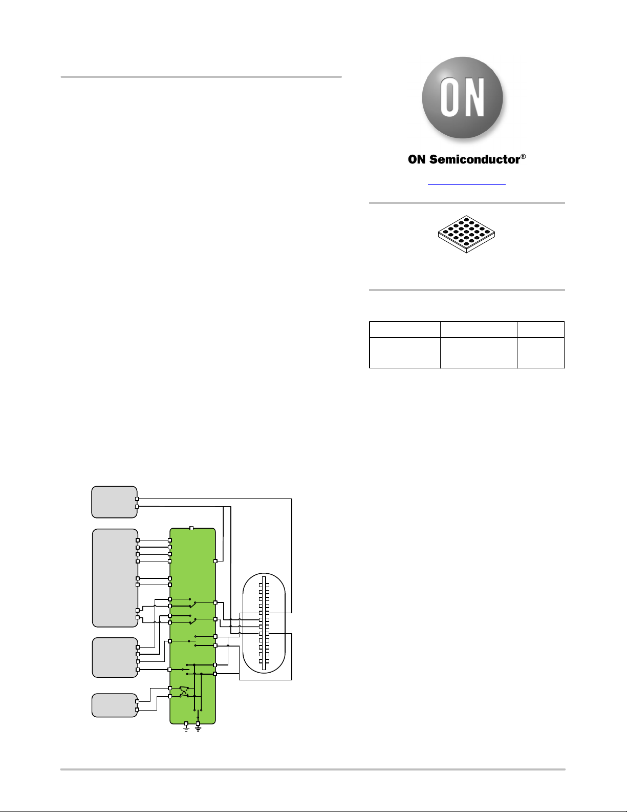
CC1
Logic
CC2
VCC
SCL
SDA
GPIO1
AP
GPIO3
INT
DN
DP
HPL
HPR
SENSE
MIC
Audio Codec
AUX+
AUX−
DP Controller
Figure 1. Application Block Diagram
SCL
SDA
ENN
DET
INT
L
DN
R
DP
SENSE
MIC
SBU2_H
SBU1_H
GND
CC_INADDRGPIO2
DN_L
DP_R
GSBU2
GSBU1
SBU2
SBU1
AGND
USB Type−C
Receptacle
GND
SSRXp1
SSRXn1
VBUS
SBU2
DN
DP
CC2
VBUS
SSTXn2
SSTXp2
GND
GND
SSTXp1
SSTXn1
VBUS
CC1
DP
DN
SBU1
VBUS
SSRXn2
SSRXp2
GND
© Semiconductor Components Industries, LLC, 2018
November, 2019 − Rev. 3
1 Publication Order Number:
FSA4480/D
Page 2
FSA4480
PIN CONFIGURATION
A
B
C
D
E
SBU 1_H
SBU 2_H
MIC
GSBU 1
GSBU 2
SBU 2
AGND
DET
CC_ IN
SENSE
SBU 1 VCC
AGND
INT
SDA
ENN
ADD R
L
DN_L
DN
GND
DP_ RSCL
R
DP
123 5
Figure 2. Pin Assignment (Top Through View)
4
www.onsemi.com
2
Page 3

FSA4480
Table 1. PIN DESCRIPTIONS
No.
1 A5 VCC Power Supply (2.7 to 5.5 V)
2 B5 GND Chip ground
3 D5 DP_R USB/Audio Common Connector
4 D4 DN_L USB/Audio Common Connector
5 E5 DP USB Data (Differential +)
6 E4 DN USB Data (Differential –)
7 C5 R Audio – Right Channel
8 C4 L Audio – Left Channel
9 A3 SBU1 Sideband use wire 1
10 A2 SBU2 Sideband use wire 2
11 C1 MIC Microphone signal
12 B2 AGND Audio signal ground
13 B3 AGND Audio signal ground
14 E2 SENSE Audio ground reference output
15 C3 INT I2C Interrupt output, active low (open drain)
16 D2 CC_IN Audio accessory attachment detection input
17 D1 GSBU1 Audio sense path 1 to headset jack GND
18 E1 GSBU2 Audio sense path 2 to headset jack GND
19 C2 DET Push−pull output. When CC_IN > 1.5 V, DET is low and CC_IN < 1.2 V, DET is high
20 D3 SCL I2C clock
21 E3 SDA I2C data
22 B1 SBU2_H Host Side Sideband Use Wire 2
23 A1 SBU1_H Host Side Sideband Use Wire 1
24 A4 ENN
25 B4 ADDR I2C slave address pin
Pin Name Description
Chip Enable, active low, internal pull−down by 470 kW
www.onsemi.com
3
Page 4
FSA4480
Table 2. ABSOLUTE MAXIMUM RATINGS
Symbol
V
CC
V
CC_IN
V
SW_C
V
SW_USB
V
SW_Audio
V
V_SBU/GSBUVSBU1
V
VSBU_H
V
I/O
V
CNTRL
I
SW_Audio
I
SW_USB
I
SW_MIC
I
SW_SBU
I
SW_SENSE
I
SW_AGND
I
IK
Supply Voltage from VCC −0.5 6.5 V
V
to GND −0.5 20 V
CC_IN,
V
DP_R
V
DP
V
to GND, V
L
to GND, V
to GND, V
to GND, V
R
to GND −3.5 20 V
DN_L
to GND −0.5 6.5 V
DN
to GND −3.6 6.5 V
to GND, V
SBU2
VSBU1_H to GND, VSBU2_H to GND −0.5 6.5 V
SENSE, MIC, DET, INT, to GND −0.5 6.5 V
Control Input Voltage SDA, SCL, ENN, ADDR −0.5 6.5 V
Switch I/O Current, Audio Path −250 250 mA
Switch I/O Current, USB Path − 100 mA
Switch I/O Current, MIC to SBU1 or SBU2 − 50 mA
Switch I/O Current, SBUx to SBUx_H − 50 mA
Switch I/O Current, SENSE to GSBU1 or GSBU2 − 100 mA
Switch I/O Current, AGND to SBU1 or SBU2 − 500 mA
DC Input Diode Current −50 − mA
ESD Human Body Model, ANSI/ESDA/JEDEC
JS−001−2012
ESD Human Body Model, ANSI/ESDA/JEDEC
JS−001−2012
ESD Charged Device Model, JEDEC: JESD22−C101 1 − kV
T
T
A
STG
Absolute Maximum Operating Temperature −40 85 °C
Storage Temperature −65 150 °C
Stresses exceeding those listed in the Maximum Ratings table may damage the device. If any of these limits are exceeded, device functionality
should not be assumed, damage may occur and reliability may be affected.
Parameter Min. Max. Unit
GSBU1
to GND, V
to GND −0.5 20 V
GSBU1
Connector side and power pins: VCC,
4 − kV
SBU1, SBU2, DP_R, DN_L, GSBU1,
GSBU2, CC_IN
Host side pins: the rest pins 2 − kV
www.onsemi.com
4
Page 5
Table 3. RECOMMENDED OPERATING CONDITIONS
Symbol
POWER
V
CC
Supply Voltage 2.7 − 5.5 V
USB SWITCH
V
SW_USB
VDP to GND, VDN to GND, V
AUDIO SWITCH
V
V
SW_Audio
DP_R
to GND, V
DN_L
MIC SWITCH
V
V
VSBU_MIC
SBU1
to GND, V
SBU2
SENSE SWITCH
V
VGSBU_SENVGSBU1
to GND, V
SBU TO SBUX_H SWITCH
V
V
VGSBU
SBU1
GND
to GND, V
SBU2
CC_IN PIN
V
V
CC_IN
to GND 0 − 5.5 V
CC_IN,
CONTROL VOLTAGE (ENN/SDA/SCL)
V
IH
Input Voltage High 1.3 − V
Parameter Min. Typ. Max. Unit
to GND, V
to GND, V
to GND, V
GSBU2
to GND, V
DP_R
to GND, V
to GND, V
L
MIC
SENSE
SBU1_H
DN_L
R
to GND 0 − 3.6 V
to GND 0 − 3.6 V
to GND, V
FSA4480
to GND 0 − 3.6 V
to GND −3.6 − 3.6 V
SBU2_H
to
0 − 3.6 V
CC
V
V
IL
Input Voltage Low − − 0.5
V
OPERATING TEMPERATURE
T
A
Ambient Operating Temperature −40 25 +85 °C
Functional operation above the stresses listed in the Recommended Operating Ranges is not implied. Extended exposure to stresses beyond
the Recommended Operating Ranges limits may affect device reliability.
www.onsemi.com
5
Page 6
FSA4480
Table 4. DC ELECTRICAL CHARACTERISTICS
(V
= 2.7 V to 5.5 V, VCC (Typ.) = 3.3 V, TA = −40°C to 85°C, and T
CC
(Typ.) = 25°C, unless otherwise specified.
A
Symbol Parameter Condition Power Min. Typ. Max. Unit
I
CC
Supply Current
USB switches on, SBUx to
SBUx_H switches on
VCC: 2.7 V to 5.5 V
Audio switches on, MIC switch on
and Audio GND switch on
I
CCZ
Quiescent Current ENN = L, 04H’b7 = 0
USB/AUDIO COMMON PINS: DP/R, DN_L
I
OZ
I
OFF
V
OV_TRIP
V
OV_HYS
Off Leakage Current of DP_R
and DN_L
Power−Off Leakage Current of
DP_R and DN_L
Input OVP Lockout
Input OVP Hysteresis
DN_L, DP_R = −3 V to 3.6 V VCC: 2.7 V to 5.5 V −3.0 − 3.0
DN_L, DP_R = 0 V to 3.6 V Power off −3.0 − 3.0
Rising edge
VCC: 2.7 V to 5.5 V
AUDIO SWITCH
I
ON
I
OFF
R
ON_AUDIO
R
SHUNT
On Leakage Current of Audio
Switch
Power−Off Leakage Current of L
and R
Audio Switch On Resistance I
Pull Down Resistor on R/L Pin
when Audio Switch is Off
DN_L, DP_R = −3 V to 3.0 V,
DP, DN, R, L
= Float
L, R = 0 V to 3 V;
DP_R, DN_L
= 100 mA, V
SW
= Float
SW
= −3 V to 3 V
VCC: 2.7 V to 5.5 V −2.5 −
Power off −1.0 − 1.0
VCC: 2.7 V to 5.5 V
L=R=3 V 6 10 14
USB SWITCH
I
I
ON
OZ
On Leakage Current of USB
Switch
DN_L, DP_R = 0 V to 3.6 V,
DP, DN, R, L
= Float
Off Leakage Current of DP andDNDN, DP = 0 V to 3.6 V −3.0 − 3.0
VCC: 2.7 V to 5.5 V
)
− 65
−
− 60
−
− 5
-
4.5 5 5.3 V
− 0.3 − V
2.5 mA
− 1.0 2.1
−3.0 − 3.0
mA
mA
mA
mA
mA
mA
W
kW
mA
mA
I
OFF
R
ON_USB
Power−Off Leakage Current of
DP and DN
USB Switch On Resistance I
SENSE SWITCH
I
ON
R
ON_SENSE
I
OZ
Sense Path Leakage Current
SENSE Switch On Resistance
Off Leakage Current of SENSE
Off Leakage Current of GSBUx
I
OFF
Power−Off Leakage Current of
SENSE
Power−Off Leakage Current of
GSBUx
DN, DP = 0 V to 3.6 V Power off −3.0 − 3.0
= 8 mA, V
SW
GSBUx = 0 V to 1 V, SENSE is
= 0.4 V VCC: 2.7 V to 5.5 V − 3.0 5.2
SW
VCC: 2.7 V to 5.5 V −2.0 − 2.0
mA
mA
floating
ISW= 100 mA, VSW =1V
Sense = 0 V to 1.0 V
VCC: 2.7 V to 5.5 V
0.20 0.30 0.40
−2.0 − 2.0
mA
GSBUx = 0 V to 1.0 V −2.0 − 2.0 mA
GSBUx = 1 V to 3.6V
Sense = 0 V to 1.0 V
GSBUx = 0 V to 3.6V
Power off
−3.0 − 3.0
−2.0 − 2.0 mA
−3.0 − 3.0
www.onsemi.com
6
W
W
Page 7
FSA4480
Table 4. DC ELECTRICAL CHARACTERISTICS (continued)
(VCC = 2.7 V to 5.5 V, VCC (Typ.) = 3.3 V, TA = −40°C to 85°C, and T
Symbol UnitMax.Typ.Min.PowerConditionParameter
SENSE SWITCH
V
OV_TRIP
V
OV_HYS
SBUX PINS
I
OZ
I
OFF
V
OV_TRIP
V
OV_HYS
MIC SWITCH
I
ON
I
OZ
I
OFF
Input OVP Lockout on GSBUx
Input OVP Hysteresis of GSBUx
Off Leakage Current of SBUx
Power−Off Leakage Current
Port SBUx
Input OVP Lockout
Input OVP Hysteresis
On Leakage Current of MIC
Switch
Off Leakage Current of MIC
Power Off Leakage Current of
MIC
Rising edge
SBUx = 0 V to 3.6 V VCC: 2.7 V to 5.5 V −3.0 − 3.0
SBUx = 0 V to 3.6 V Power off −3.0 − 3.0
Rising edge
SBUx = 0 V to 3.6 V,
MIC is floating
MIC = 0 V to 3.6 V −1.0 − 1.0
MIC = 0 V to 3.6 V Power off −1.0 − 1.0
(Typ.) = 25°C, unless otherwise specified.
A
VCC: 2.7 V to 5.5 V
VCC: 2.7 V to 5.5 V
VCC: 2.7 V to 5.5 V
)
4.5 5 5.3 V
− 0.3 − V
4.5 5 5.3 V
− 0.3 − V
−3.0 − 3.0
mA
mA
mA
mA
mA
R
ON_MIC
MIC Switch On Resistance
SBUX_H SWITCH
I
ON
I
OZ
I
OFF
R
ON_SBU
On Leakage Current of SBUx_H
Switch
Off Leakage of SBUx_H
Power Off Leakage Current of
SBUx_H
SBUx_H Switch On Resistance
AUDIO GROUND SWITCH: PIN: AGND TO SBUX
R
ON_AGND
AGND Switch On Resistance
CC_IN PIN
V
V
TH_L
TH_H
I
IN
Input Low Threshold
Input High Threshold
Input Leakage of CC_IN
INT, DET PINS
V
OH
Output High for DET
Isw = 30 mA, VSW = 3.6 V VCC: 2.7 V to 5.5 V 1.7 3.0 3.9
SBUx = 0 V to 3.6 V, SBUx_H is
VCC: 2.7 V to 5.5 V
−3.0
−
3.0 mA
floating
SBUx_H =0 V to 3.6 V
−1
− 1
SBUx_H = 0 V to 3.6 V Power off −1.0 − 1.0
Isw = 30 mA, VSW= 0 V to 3.6 V VCC: 2.7 V to 5.5 V 1.5 3.0 3.5
SOURCE
= 100 mA on SBUx VCC: 2.7 V to 5.5 V 30 50 90
VCC: 2.7 V to 5.5 V
− 1.2 − V
I
− 1.5 − V
CC_IN = 0 V to 5.5 V − − 1.0
Io = −2mA
VCC: 2.7 V to 5.5 V
1.5 1.8 2 V
W
mA
mA
W
mW
mA
V
OL
Output Low for DET and INT
Io = 2 mA − − 0.4 V
www.onsemi.com
7
Page 8
FSA4480
Table 4. DC ELECTRICAL CHARACTERISTICS (continued)
(VCC = 2.7 V to 5.5 V, VCC (Typ.) = 3.3 V, TA = −40°C to 85°C, and T
Symbol UnitMax.Typ.Min.PowerConditionParameter
ADDR PIN
V
IH
V
IL
I
IN
ENN PIN
V
IH
V
IL
R
PD
SDS, SCL PINS
V
ILI2C
V
IHI2C
I
I2C
Input voltage High
Input voltage Low
Control Input Leakage
Input Voltage High
Input Voltage Low
Internal Pull Down Resistor
Low−Level Input Voltage
High−Level Input Voltage
Input Current of SDA and SCL
Pins
ADDR = 0 V to V
SCL/SDA = 0 V to 3.6 V −2 − 2
(Typ.) = 25°C, unless otherwise specified.
A
VCC: 2.7 V to 5.5 V
CC
VCC: 2.7 V to 5.5 V
VCC: 2.7 V to 5.5 V
)
1.3 − − V
− − 0.45 V
− 1
−1
1.3 − − V
− − 0.45 V
− 470 −
− − 0.4 V
1.2 − − V
mA
kW
mA
V
OLSDA
I
OLSDA
Low−Level Output Voltage
Low−Level Output Current
IOL=2mA − − 0.3 V
V
OLSDA
= 0.2 V
10
− − mA
Product parametric performance is indicated in the Electrical Characteristics for the listed test conditions, unless otherwise noted. Product
performance may not be indicated by the Electrical Characteristics if operated under different conditions.
www.onsemi.com
8
Page 9
FSA4480
Table 5. AC ELECTRICAL CHARACTERISTICS
(V
= 2.7 V to 5.5 V, VCC (Typ.) = 3.3 V, TA = −40°C to 85°C, and T
CC
(Typ.) = 25°C, unless otherwise specified.
A
Symbol Parameter Condition Power Min. Typ. Max. Unit
AUDIO SWITCH
t
t
X
delay
t
rise
OFF
TAL K
Audio Switch Turn On Delay Time DP_R = DN_L = 1 V,
Audio Switch Turn On Rising Time
(Note 1)
Audio Switch Turn Off Time DP_R = DN_L = 1 V,
Cross Talk (Adjacent)
BW −3 dB Bandwidth
O
IRR
Off Isolation
THD+N Total Harmonic Distortion + Noise
Performance with A−weighting Filter
= 32 W
R
L
DP_R = DN_L = 1 V,
= 32 W
R
L
= 32 W
R
L
= 1 V
L
RMS
= 50 W,
f = 1 kHz, R
V
SW
RL = 50 W
F = 1 kHz, RL = 50 W,
C
L = 0 pF, VSW = 1 VRMS
R
= 600 W, f = 20 Hz~20 kHz,
L
V
= 2 V
SW
R
L
V
SW
R
L
V
SW
RMS
= 32 W, f = 20 Hz~20 kHz,
= 1 V
RMS
= 16 W, f = 20 Hz~20 kHz,
= 0.5 V
RMS
VCC = 3.3 V
USB SWITCH
t
ON
t
OFF
BW
USB Switch Turn−on Time DP_R = DN_L = 1.5 V,
R
= 50 W
L
USB Switch Turn −off Time DP_R = DN_L = 1.5 V,
R
= 50 W
L
−3 dB Bandwidth R
= 50 W − 850 −
L
VCC = 3.3 V
SDD21 −3 dB Bandwidth − 950 −
O
t
IRR
OVP
Off Isolation between DP, DN and Common Node Pins
DP_R and DN_L pins OVP Response
Time
f = 1 kHz, RL = 50 W, CL = 0 pF,
VSW = 1 VRMS
Vsw = 3.5 V to 5.5 V − 1 1.5
MIC/AUDIO GROUND SWITCH
t
delay_MIC
t
rise_MIC
t
delay_AGND
t
rise_AGND
t
OFF_MIC
t
OFF_Audio GND
MIC Switch Turn On Delay Time SBUx = 1 V, R
MIC Switch Turn On Rising Time
(Note 1)
AGND Switch Turn On Time
AGND Switch Turn On Rising Time
(Note 1)
MIC Switch Turn Off Time
AGND Switch Turn Off Time SBUx: Isource = 10 mA,
BW MIC Switch Bandwidth
= 50 W
L
SBUx pulled up to 0.5 V by
16 W, AGND connect to GND
SBUx = 2.5 V, R
= 50 W
L
clamp to 2.5 V
R
= 50 W
L
VCC = 3.3 V
VCC = 3.3 V
)
− 65 −
−
240
−
− 15 −
− −100 − dB
− 600 − MHz
− −100 − dB
− −110 − dB
− −110 − dB
− −108 − dB
− 60 −
− 15 −
− −100 − dB
− 100 − ms
−
250
−
− 100 − ms
− 1500 −
− 15 −
− 15 −
− 50 − MHz
ms
ms
ms
ms
ms
MHz
ms
www.onsemi.com
9
Page 10

FSA4480
Table 5. AC ELECTRICAL CHARACTERISTICS (continued)
(VCC = 2.7 V to 5.5 V, VCC (Typ.) = 3.3 V, TA = −40°C to 85°C, and T
Symbol UnitMax.Typ.Min.PowerConditionParameter
SBUX_H SWITCH
t
ON
tOFF SBUx_H Switch Turn Off Time
BW Bandwidth
t
OVP
SENSE SWITCH
t
delay
t
rise
tOFF Sense Switch Turn Off Time
t
OVP
BW Bandwidth
DET DELAY
SBUx_H Switch Turn On Time SBUx = 2.5 V, R
R
= 50 W
L
SBUx Pins OVP Response Time
Sense Switch Turn On Delay Time
Vsw = 3.5 V to 5.5 V − 0.5 1
GSBUx = 1 V, R
Sense Switch Turn On Rising Time
(Note 1)
GSBUx Pins OVP Response Time
VSW: 3.5 V to 5.5 V −
R
= 50 W
L
(Typ.) = 25°C, unless otherwise specified.
A
= 50 W
L
= 50 W
L
VCC = 3.3 V
VCC = 3.3 V
)
− 35 − ms
− 15 −
− 50 MHz
ms
− 65 −
− 260 −
− 15 −
0.7
1.5
ms
ms
ms
ms
− 150 − MHz
t
DELAY_DET
DET Response Delay
1. Turn on timing can be controlled by I2C register.
Transition from 0 to 1.8 V
VCC = 3.3 V
− 1 − ms
Transition from 1.8 to 0 V − 5 −
www.onsemi.com
10
Page 11

FSA4480
Table 6. I2C SPECIFICATION
(VCC = 2.7 V to 5.5, V
Symbol
f
SCL
t
HD; STA
t
LOW
t
HIGH
t
SU; STA
t
HD; DAT
t
SU; DAT
t
r
t
f
t
SU; STO
t
BUF
t
SP
2. Guaranteed by design, not production tested.
3. A fast−mode I
is automatically the case if the device does not stretch the LOW period of the I2C_SCL signal. If such a device does stretch the LOW period
2
C_SCL signal, it must output the next data bit to the I2C_SDA line t
of the I
standard−mode I
(Typ.) = 3.3 V ,TA = −40°C to 85°C. T
CC
Parameter
I2C_SCL Clock Frequency 400 kHz
Hold Time (Repeated) START Condition 0.6
Low Period of I2C_SCL Clock 1.3
High Period of I2C_SCL Clock 0.6
Set−up Time for Repeated START Condition 0.6
Data Hold Time (Note 2) 0 0.9
Data Set−up Time (Note 3) 100 ns
Rise Time of I2C_SDA and I2C_SCL Signals (Note 3) 20 + 0.1C
Fall Time of I2C_SDA and I2C_SCL Signals (Note 3) 20 + 0.1C
Set−up Time for STOP Condition 0.6
Bus−Free Time between STOP and START Conditions 1.3
Pulse Width of Spikes that Must Be Suppressed by the Input Filter 0 50 ns
2
C−bus device can be used in a standard−mode I2C−bus system, but the requirement t
2
C bus specification) before the I2C_SCL line is released.
(Typ.) = 25°C, unless otherwise specified)
A
r_max
+ t
= 1000 + 250 = 1250 ns (according to the
SU;DAT
Fast Mode
Min. Max. Unit
300 ns
b
300 ns
b
≥ ±250 ns must be met. This
SU;DAT
ms
ms
ms
ms
ms
ms
ms
Figure 3. Definition of Timing for Full−Speed Mode Devices on the I2C Bus
www.onsemi.com
11
Page 12

Table 7. CAPACITANCE
(6)
(6)
(6)
(6)
(VCC= 2.7 V to 5.5 V, V
Symbol
C
ON_USB/Audio
C
OFF_ USB/Audio
C
OFF_USB
C
ON_SENSE_SW
C
OFF_SENSE_SW
C
ON_MIC_SW
C
OFF_MIC_SW
C
ON_AGND_SW
C
ON_SBUx_H_SW
C
CNTRL
(Typ.) = 3.3 V, T
CC
On Capacitance
(Common Port)
Off Capacitance
(Common Port)
Off Capacitance
(Non−Common Ports)
On Capacitance −
(Common Ports)
Off Capacitance −
(Common Ports)
On Capacitance −
(Common Ports)
Off Capacitance −
(Common Ports)
On Capacitance
(Common Port)
On Capacitance
(Common Port)
Control Input Pin
Capacitance
FSA4480
= −40°C to 85°C, and TA (Typ.) = 25°C)
A
Parameter Condition Power
(6)
(6)
(6)
(6)
(6)
f = 1 MHz, 100 mV
bias
f = 1 MHz, 100 mV
bias
f = 1 MHz, 100 mV
(6)
bias
f = 1 MHz, 100 mV
DC bias
f = 1 MHz, 100 mV
DC bias
f = 1 MHz, 100 mV
DC bias
f = 1 MHz, 100 mV
DC bias
f = 1 MHz, 100 mV
DC bias
f = 1 MHz, 100 mV
DC bias
f = 1 MHz,
100 mV
DC bias
, 100 mV
PP
, 100 mV DC
PK−PK
, 100 mV DC
PK−PK
, 100 mV DC
PK−PK
, 100 mV
PK−PK
, 100 mV
PK−PK
, 100 mV
PK−PK
, 100 mV
PK−PK
, 100 mV
PK−PK
, 100 mV
PK−PK
ENN 3 pF
VCC = 3.3 V
T
=− 40°C to +85°C
A
Min. Typ. Max.
9 pF
7.5 pF
3 pF
55 pF
88 pF
170 pF
10 pF
125 pF
160 pF
Unit
Table 8. REGISTER MAPS
Reset
ADDR Register Name Type
00H Device ID R 0x09 0 0 0 0 1 0 0 1
01H OVP
02H OVP interrupt
03H OVP status R 0x00 Reserved OVP/
04H Switch settings
05H Switch select R/W 0x18 Reserved SBU1_H
06H Switch Status0 R 0x00 Reserved Sense Switch Status DP_R Switch Status DN_L Switch Status
07H Switch Status1 R 0x00 Reserved SBU2 Switch Status SBU1 Switch Status
08H Audio Switch Left
09H Audio Switch
0AH MIC switch turn
0BH Sense switch
0CH Audio Ground
Interrupt Mask
flag
Enable
Channel turn on
Control
Right Channel
turn on Control
on control
turn on control
Switch turn on
Control
R/W 0x00 Reserved Mask
R/C 0x00 Reserved DP_R DN_L SBU1 SBU2 GSBU GSBU2
R/W 0x98 Device
R/W 0x01 Audio switch left channel slow control [7:0]
R/W 0x01 Audio switch right channel slow control [7:0]
R/W 0x01 MIC switch right channel slow control [7:0]
R/W 0x01 Sense switch right channel slow control [7:0]
R/W 0x01 Audio ground switch right channel slow control [7:0]
Value
BIT7 BIT6 BIT5 BIT4 BIT3 BIT2 BIT1 BIT0
control
OVP
interrupt
SBU1_H
to SBUx
to SBUx
Mask
OVP
/DP_R
DP_R
SBU2_H
to SBUx
SBU2_H
to SBUx
Mask
OVP
/DN_L
OVP/
DN_L
DN_L to
DN or L
DN_L to
DN or L
Mask
OVP
/SBU1
OVP/SBU1OVP/SB
DP_R to
DP or R
DP_R to
DP or R
Mask
OVP
/SBU2
U2
Sense to
GSBUx
Sense to
GSBUx
Mask
OVP
/GSBU1
OVP/
GSBU1
MIC to
SBUx
MIC to
SBUx
Mask
OVP
/GSBU2
OVP/
GSBU2
Audio
Ground
to SBUx
Audio
Ground
to SBUx
www.onsemi.com
12
Page 13

FSA4480
Table 8. REGISTER MAPS
Reset
ADDR BIT0BIT1BIT2BIT3BIT4BIT5BIT6BIT7
0DH Timing Delay
0EH Timing Delay
0FH Timing Delay
10H Timing Delay
11H Audio accessory
12H Function enable R/W 0x08 Reserved DET I/O
13H RES detection
14H RES detection
15H
16H RES detection
17H Audio jack Status RO 0x01 Reserved 4pole,SB
18H Detection
19H Detection
1AH Audio detection
1BH Audio detection
1CH MIC Threshold
1DH MIC Threshold
1EH I2C Reset W/C 0x00 Reserved I2C reset
1FH Current Source
between R
switch enable
and L switch
enable
between MIC
switch enable
and L switch
enable
between Sense
switch enable
and L switch
enable
between Audio
ground switch
enable and L
switch enable
status
pin setting
value
RES detection
interrupt
threshold
interval
interrupt
interrupt Mask
RGE1
RGE2
DATA0
DATA1
Setting
TypeRegister Name
R/W 0x00 Timing Delay between R switch enable and L switch enable control [7:0]
R/W 0x00 Timing Delay between MIC switch enable and L switch enable control [7:0]
R/W 0x00 Timing Delay between Sense switch enable and L switch enable control [7:0]
R/W 0x00 Timing Delay between Audio ground switch enable and L switch enable control [7:0]
R 0x02 Reserved CC_IN DET
R/W 0x00 Reserved Detection pin select [2:0]
R 0xFF R detection value [7:0]
R/W 0x16 R detection Interrupt resistance threshold [7:0]
R/W 0X00 Reserved Detection interval [1:0]
R/C 0x00 Reserved Audio
R/W 0x00 Reserved Audio
RO 0xFF audio detection value REG1 [7:0]
RO 0xFF audio detection value REG2 [7:0]
R/W 0x20 MIC Threshold value DATA0 [7:0]
R/W 0xFF MIC Threshold value DATA1 [7:0]
R/W 0x07 Reserved Current Source setting [3:0]
Value
Control
RES
detection
range
setting
GIPO
control
SLOW
TURN−O
N
CONTR
OLL
U2 MIC
MIC auto
control
4pole,SB
U1 MIC
detection
done
detection
done
mask
RES
detection
: auto
clear
3pole No audio
RES
detection
occurred
RES
detection
occurred
mask
Audio
jack
detection
: auto
clear
RES
detection
done
RES
detection
done
mask
Table 9. I2C SLAVE ADDRESS
ADDR Bit 7 Bit 6 Bit 5 Bit 4 Bit 3 Bit 2 Bit 1 Bit 0
ADDR = L 1 0 0 0 0 1 0 R/W
ADDR = H 1 0 0 0 0 1 1 R/W
www.onsemi.com
13
Page 14

FSA4480
DEVICE ID
Address: 00h
Reset Value: 8’b 0000_1001
Type: Read
Bits
7:6 Vendor ID 2 Vendor ID
5:3 Version ID 3 Device Version ID
2:0 Revision ID 3 Revision History ID
OVP INTERRUPT MASK
Address: 01h
Reset Value: 8’b 0000_0000
Type: Read/Write
Bits
7 Reserved 1 Do Not Use
6 OVP Interrupt mask control 1 OVP Interrupt function Enable/Disable
5 DP_R OVP Interrupt mask control 1 0: Do not mask OVP interrupt
4 DN_L OVP Interrupt mask control 1 0: Do not mask OVP interrupt
3 SBU1 OVP Interrupt mask control 1 0: Do not mask OVP interrupt
2 SBU2 OVP Interrupt mask control 1 0: Do not mask OVP interrupt
1 GSBU1 OVP Interrupt mask control 1 0: Do not mask OVP interrupt
0 GSBU2 OVP Interrupt mask control 1 0: Do not mask OVP interrupt
Name Size Description
Name Size Description
0: Controlled by [5:0] bit
1: Mask all connector side pins OVP interrupt
1: Mask OVP interrupt
1: Mask OVP interrupt
1: Mask OVP interrupt
1: Mask OVP interrupt
1: Mask OVP interrupt
1: Mask OVP interrupt
OVP INTERRUPT FLAG
Address: 02h
Reset Value: 8’b 0000_0000
Type: Read Clear
Bits
[7:6] Reserved 2 Do Not Use
5 DP_R OVP 1 0: OVP event has not occurred
4 DN_L OVP 1 0: OVP event has not occurred
3 SBU1 OVP 1 0: OVP event has not occurred
2 SBU2 OVP 1 0: OVP event has not occurred
1 GSBU1 OVP 1 0: OVP event has not occurred
0 GSBU2 OVP 1 0: OVP event has not occurred
Name Size Description
1: OVP event has occurred
1: OVP event has occurred
1: OVP event has occurred
1: OVP event has occurred
1: OVP event has occurred
1: OVP event has occurred
www.onsemi.com
14
Page 15

FSA4480
OVP STATUS
Address: 03h
Reset Value: 8’b 0000_0000
Type: Read
Bits
[7:6] Reserved 2 Do Not Use
5 OVP on DP_R PIN 1 0: OVP event has not occurred
4 OVP on DN_L PIN 1 0: OVP event has not occurred
3 OVP on SBU1 PIN 1 0: OVP event has not occurred
2 OVP on SBU2 PIN 1 0: OVP event has not occurred
1 OVP on GSBU1 PIN 1 0: OVP event has not occurred
0 OVP on GSBU2 PIN 1 0: OVP event has not occurred
SWITCHING SETTING ENABLE
Address: 04h
Reset Value: 8’b 1001_1000
Type: Read/Write
Bits
7 Device Enable 1 0: Device Disable; L, R pull down by 10 k and other switch
6 SBU1_H to SBUx switches 1 0: Switch Disable; SBU1_H will be high−Z for positive input
5 SBU2_H to SBUx switches 1 0: Switch Disable; SBU2_H will be high−Z for positive input
4 DN_L to DN or L switches 1 0: Switch Disable; DN_L,DN will be high−Z for positive input. L
3 DP_R to DP or R switches 1 0: Switch Disable; DP_R,DP will be high−Z for positive input.
2 Sense to GSBUx switches 1 0: Switch Disable; Sense,GSBU1 and GSBU2 will be high−Z for
1 MIC to SBUx switches 1 0: Switch Disable: MIC will be high−Z for positive input.
0 AGND to SBUx switches 1 0: Switch Disable: AGND will be high−Z for positive input.
Name Size Description
1: OVP event has occurred
1: OVP event has occurred
1: OVP event has occurred
1: OVP event has occurred
1: OVP event has occurred
1: OVP event has occurred
Name Size Description
nodes will be high−Z for positive input.
1: Device Enable.
Device Enable = 1 Device enable = 0
ENN = 1 Device Disable Device Disable
ENN = 0 Device Enable Device Disable
1: Switch Enable
1: Switch Enable
pull down by 10 kohm
1: Switch Enable
R pull down by 10 kohm
1: Switch Enable
positive input
1: Switch Enable
1: Switch Enable
1: Switch Enable
www.onsemi.com
15
Page 16

FSA4480
SWITCH SELECT
Address: 05h
Reset Value: 8’b 0001_1000
Type: Read/Write
Bits
7 Reserved 1 Do Not Use
6 SBU1_H switches 1 0: SBU1_H to SBU1 switch ON
5 SBU2_H switches 1 0: SBU2_H to SBU2 switch ON
4 DN_L to DN or L switches 1 0: DN_L to L switch ON
3 DP_R to DP or R switches 1 0: DP_R to R switch ON
2 Sense to GSBUx switches 1 0: Sense to GSBU1 switch ON
1 MIC to SBUx switches 1 0: MIC to SBU2 switch ON
0 AGND to SBUx switches 1 0: AGND to SBU1 switch ON
Name Size Description
1: SBU1_H to SBU2 switch ON
1: SBU2_H to SBU1 switch ON
1: DN_L to DN switch ON
1: DP_R to DP switch ON
1: Sense to GSBU2 switch ON
1: MIC to SBU1 switch ON
1: AGND to SBU2 switch ON
SWITCH STATUS0
Address: 06h
Reset Value: 8’b 0000_0000
Type: Read Only
Bits
[7:6] Reserved 2 Do not use
[5:2] Sense Switch Status 2 00: Sense switch is Open/Not Connected
[3:2] DP_RSwitch Status 2 00: DP_R Switch Open/Not Connected
[1:0] DN_L switch Status 2 00: DN_L Switch Open/Not Connected
Name Size Description
01: Sense connected to GSBU1
10: Sense connected to GSBU2
11: Not Valid
01: DP_Rconnected to DP
10: DP_Rconnected to R
11: Not Valid
01: DN_L connected to DN
10: DN_L connected to L
11: Not Valid
www.onsemi.com
16
Page 17

FSA4480
SWITCH STATUS1
Address: 07h
Reset Value: 8’b 0000_0000
Type: Read Only
Bits
[7:6] Reserved 2 Do not use
[5:3] SBU2 Switch Status 3 000: SBU2 switch is Open/Not Connected
[2:0] SBU1 Switch Status 3 000: SBU1 switch is Open/Not Connected
AUDIO SWITCH LEFT CHANNEL SLOW TURN−ON
Address: 08h
Reset Value: 8’b 0000_0001
Type: Read/Write
Bits
[7:0] Switch turn on rising time setting 8
Name Size Description
001: SBU2 connected to MIC
010: SBU2 connected to AGND
011: SBU2 connected to SBU1_H
100: SBU2 connected to SBU2_H
101: SBU2 connected both SBU1_H and SBU2_H
110 …111: Do not use
001: SBU1 connected to MIC
010: SBU1 connected to AGND
011: SBU1 connected to SBU1_H
100: SBU1 connected to SBU2_H
101: SBU1 connected both SBU1_H and SBU2_H
110 …111: Do not use
Name Size Description
11111111: 256 00 mS
…
00000001: 200 mS
00000000: 100 mS
AUDIO SWITCH RIGHT CHANNEL SLOW TURN−ON
Address: 09h
Reset Value: 8’b 0000_0001
Type: Read/Write
Bits
[7:0] Switch turn on rising time setting 8
Name Size Description
MIC SWITCH SLOW TURN−ON
Address: 0Ah
Reset Value: 8’b 0000_0001
Type: Read/Write
Bits
[7:0] Switch turn on rising time setting 8
Name Size Description
11111111: 256 00 mS
…
00000001: 200 mS
00000000: 100 mS
11111111: 257 00 mS
…
00000010: 350 mS
00000001: 250 mS
00000000: Not Valid
www.onsemi.com
17
Page 18

SENSE SWITCH SLOW TURN−ON
Address: 0Bh
Reset Value: 8’b 0000_0001
Type: Read/Write
Bits
[7:0] Switch turn on rising time setting 8
Name Size Description
AUDIO GROUND SWITCH SLOW TURN−ON
Address: 0Ch
Reset Value: 8’b 0000_0001
Type: Read/Write
Bits
[7:0] Switch turn on rising time setting 8
Name Size Description
FSA4480
11111111: 256 00 mS
…
00000001: 200 mS
00000000: 100 mS
11111111: 179000 mS
…
00000001: 1400 mS
00000000: 700 mS
TIMING DELAY BETWEEN R SWITCH ENABLE AND L SWITCH ENABLE
Address: 0Dh
Reset Value: 8’b 0000_0000
Type: Read/Write
Bits
[7:0] Delay timing setting 8
Name Size Description
11111111: 255 00 mS
11111110: 25400 mS
…
00000001: 100 mS
00000000: 0 mS
TIMING DELAY BETWEEN MIC SWITCH ENABLE AND L SWITCH ENABLE
Address: 0Eh
Reset Value: 8’b 0000_0000
Type: Read/Write
Bits
[7:0] Delay timing setting 8
Name Size Description
11111111: 255 00 mS
11111110: 25400 mS
…
00000001: 100 mS
00000000: 0 mS
www.onsemi.com
18
Page 19

FSA4480
TIMING DELAY BETWEEN SENSE SWITCH ENABLE AND L SWITCH ENABLE
Address: 0Fh
Reset Value: 8’b 0000_0000
Type: Read/Write
Bits
[7:0] Delay timing setting 8
TIMING DELAY BETWEEN AUDIO GROUND SWITCH ENABLE AND L SWITCH ENABLE
Address: 10h
Reset Value: 8’b 0000_0000
Type: Read/Write
Bits
[7:0] Delay timing setting 8
Name Size Description
11111111: 255 00 mS
11111110: 25400 mS
…
00000001: 100 mS
00000000: 0 mS
Name Size Description
11111111: 255 00 mS
11111110: 25400 mS
…
00000001: 100 mS
00000000: 0 mS
AUDIO ACCESSORY STATUS
Address: 11h
Reset Value: 8’b 0000_0010
Type: Read
Bits
[7:2] Reserved 6 Do not use
1 CC_IN 1 0: CC_IN < 1.2 V
0 DET 1 0: DET output is low
Name Size Description
1: CC_IN > 1.5 V
1: DET is output is high
www.onsemi.com
19
Page 20

FSA4480
FUNCTION ENABLE
Address: 12h
Reset Value: 8’b 0000_1000
Type: Read/Write
Bits
7 Reserved 1 Do not use
6 DET I/O Control 1 1: DET pin is in Open/Drain Configuration
5 RES detection range setting 1 1: 10k to 2560 k
4 GPIO control enable 1 1: enable
3 Slow turn on control enable 1 1: enable
2 MIC auto break out control enable 1 1: enable
1 RES detection enable 1 1: enable; will be changed to ‘0’ after low resistance detection
0 Audio jack detection and
Name Size Description
0: DET pin is in Push/Pull Configuration
0: 1k to 256 k
0: disable
0: disable
0: disable
0: disable
configuration enable
1 1: enable; will be changed to ‘0’ after audio jack detection and
configuration
0: disable
When GPIO control mode (manual switch control) is enable. ‘Switch control’ register is changed to read only. It will reflect
switch status. I
RES DETECTION PIN SETTING
Address: 13h
Reset Value: 8’b 0000_0000
Type: Read
Bits
[7:3] Reserved 5 Do not use
[2:0] Pin selection 3 000: CC_IN
2
C slave address is
Name Size Description
001: DP/R
010: DN_L
011: SBU1
100: SBU2
101: Do not use
…
111: Do not use
If RES detection pin is enable before setting PIN selection it will always do the CC_IN first. Recommend user to select the
pin first before setting the RES detection pin enable.
RES VALUE
Address: 14h
Reset Value: 8’b 1111_1111
Type: Read
Bits
[7:0] Detected resistance value 8 0000_0000 : R < 1 k
Name Size Description
…
1111_1111: R > 300 K
www.onsemi.com
20
Page 21

FSA4480
RES DETECTION THRESHOLD
Address: 15h
Reset Value: 8’b 0001_0110
Type: Read
Bits
[7:0] RES detection threshold 8
RES DETECTION INTERVAL
Address: 16h
Reset Value: 8’b 0000_0000
Type: Read
Bits
[7:2] Reserved 6 Do not use
[1:0] RES detection interval 2 00: Single
Name Size Description
Selection by 1 KW per step if Reg 12h [5] = 0
Selection by 10 KW per step if Reg 12h [5] = 0
Default Value = 22 KW
0000_0000: 1 KW /10 KW
…
1111_1111: 256 KW / 2560 KW
Name Size Description
01: 100 mS
10: 1 S
11: 10 S
AUDIO JACK STATUS
Address: 17h
Reset Value: 8’b 0000_0001
Type: Read
Bits
[7:3] Reserved 4 Do not use
3 4pole 1 1: 4 Pole SBU2 to MIC, SBU1 to audio ground
2 4pole 1 1: 4 Pole SBU1 to MIC, SBU2 to audio ground
1 3 pole 1 1: 3 pole
0 No audio accessory 1 1: No audio accessory
Name Size Description
0: others
0: others
0: others
0: Audio accessory attached
RES DETECTION /AUDIO JACK DETECTION INTERRUPT FLAG
Address: 18h
Reset Value: 8’b 0000_0000
Type: Read Clear
Bits
[7:3] Reserved 5 Do Not Use
2 Audio jack detection and
1 Low resistance occurred 1 0: Low resistance has not occurred
0 Low resistance detection 1 0: Low resistance has not occurred
Name Size Description
configuration
1 0: Audio jack detection and configuration has not occurred
1: Audio jack detection and configuration has occurred
1: Low resistance has occurred
1: Low resistance has occurred
www.onsemi.com
21
Page 22

FSA4480
RES /AUDIO JACK DETECTION INTERRUPT MASK
Address: 19h
Reset Value: 8’b 0000_0000
Type: Read Clear
Bits
[7:3] Reserved 5 Do Not Use
2 Audio jack detection and
1 Low resistance occurred 1 1: Low resistance has occurred interrupt
0 Low resistance detection 1 1: Low resistance detection has occurred interrupt
AUDIO JACK DETECTION REG1 VALUE
Address: 1Ah
Reset Value: 8’b 1111_1111
Type: Read
Bits
[7:0] Audio jack detection value 8 Resistance between SBU1 to SBU2
AUDIO JACK DETECTION REG2 VALUE
Address: 1Bh
Reset Value: 8’b 1111_1111
Type: Read
Bits
[7:0] Audio jack detection value 8 Resistance between SBU2 to SBU1
Name Size Description
configuration
Name Size Description
Name Size Description
1 1: Mask Audio jack detection and configuration has occurred
interrupt
MIC DETECTION THRESHOLD DATA0
Address: 1Ch
Reset Value: 8’b 0010_0000
Type: Read/Write
Bits
[7:0] MIC detection threshold DATA0 8 MIC detection threshold DATA0
Name Size Description
0010_0000: 300 mV
MIC DETECTION THRESHOLD DATA1
Address: 1Dh
Reset Value: 8’b 1111_1111
Type: Read/Write
Bits
[7:0] MIC detection threshold DATA1 8 MIC detection threshold DATA1
Name Size Description
1111_1111: 2.4 V
I2C RESET
Address: 1Eh
Reset Value: 8’b 0000_0000
Type: W/C
Bits
[7:1] Reserved 7 Reserved
0 I2C reset 1 0: default
Name Size Description
2
1: I
C reset
www.onsemi.com
22
Page 23

FSA4480
CURRENT SOURCE SETTING
Address: 1Fh
Reset Value: 8’b 0000_0111
Type: Write
Bits
[7:4] Reserved 4 Reserved
[3:0] Current Source Setting 4
Name Size Description
1111: 1500 mA
0111: 700 mA
0001: 100 mA
0000: invalid
www.onsemi.com
23
Page 24

FSA4480
APPLICATION INFORMATION
Over−Voltage Protection
FSA4480 features over−voltage protection (OVP) on
receptacle side pins that switches off the internal signal
routing path if the input voltage exceeds the OVP threshold.
If OVP is occurred, interrupt signal can be send by INT
signal and FLAG data will provide information that which
pin had OVP event.
Device Disable Device Enable
CC_IN < V
CC_IN > V
= 1.2 V DET = 0 DET = 1
TH_L
= 1.5 V DET = 0 DET = 0
TH_H
MIC Switch Auto−off Function
The function is active during control bit 0x12h bit[2] = 1.
When CC_IN is high (CC_IN > 1.5 V) and L,R, Audio
ground switches are under on status, MIC switch will be off
and receptacle side pin will be connected to ground for 50 mS
first. Then it shows high−Z status under MIC switch is set on
status.
Audio Jack detection
and configuration Start
Headset Detection
FSA4480 integrates headset unplug detection function by
detecting the CC_IN voltage. The function is always active
when device is enabling. DET will be high when CC_IN is
low (CC_IN < 1.2 V). When CC_IN = High (CC_IN > 1.5
V), DET will be released to low.
Audio Ground Detection and Configuration
The function is active when control bit 0x12h bit[0] = 1
and R, L AGND switches are set to be on status. For type−C
interface analog headset, the audio ground could be SBU1
pin or SBU2 pin. The function will provide autonomous
detection and configuration to route MIC and audio ground
signal accordingly.
REG2>= DATA1
and
REG1>=DATA1
Hold current setting
REG2>REG1>DATA0
&& REG1<DATA1
Or
REG2>DATA0>REG1
MIC to SBU2,
Audio ground to SBU1
Sense to GSBU1
send INT
Figure 4.
During detection and configuration, the R, L, Sense, MIC
and Audio ground switch will be off. After detection and
configuration, R and L switches will turn on according to
REG1>REG2>DATA0
&& REG2<DATA1
Or
REG1>DATA0>RGE2
MIC to SBU1,
Audio ground to SBU2
Sense to GSBU2
send INT
DATA0>=REG1
and
DATA0>=REG2
Audio ground to SBU1
Sense to GSBU1
SBU2 switch open
switch configuration and timing setting. MIC, Sense and
Audio ground will turn on according to detection results and
timing control setting.
www.onsemi.com
24
Page 25

FSA4480
Resistance Detection
The function is active during control bit 0x12h bit[1] = 1.
It will monitor the resistance between receptacle side pins
and ground. During resistance detection, the switch which
is monitored will be off. The detection result will be saved
RES Detection Start
Enable RES Detection on
SBU2
Enable RES Detection on
SBU1
Enable RES Detection on
CC_IN
Update RES value
register
And compare with
threshold
<threshold
Send INT
Disable resistance
detection
Figure 5.
in the resistance flag register. The measurement could be
from 1 kW to 2.56 MW which is controlled by internal
register. The detection interval can be set at 100 ms, 1 s or
10 s by register 0x16h.
Enable RES Detection on
DP/R
>threshold
If interval reg
Yes
= 0
Enable RES Detection on
DP/L
Wait timer that set by
interval reg
and check
0x12 bit[2]= 1?
No
Manual Switch Control
The function is active during control bit 0x12h bit[4] = 1
During this configuration, ADDR and INT pins will be set
as logic control input.
and 0x04h = FF. It will provide manual control for device.
MANUAL SWITCH CONTROL
(The function is active during control bit 0x12h bit[4] = 1 and 0x04h = FF. It will provide manual control for device. During this
configuration, ADDR and INT pins will be set as logic control input.)
Power ENN ADDR INT
OFF X X X OFF OFF OFF OFF OFF OFF
ON H X X OFF OFF OFF OFF OFF OFF
ON L 0 0 OFF OFF ON:
ON L 0 1 OFF OFF ON:
ON L 1 0 ON
ON L 1 1 ON
SENSE
Switch
GSBU2 to
SESNE
GSBU1 to
SESNE
Headset
Detection
ON OFF ON:
ON OFF ON:
USB Switch Audio Switch
DP_R to DP
DN_L to DN
DP_R to DP
DN_L to DN
MIC/ Audio
GND Switch
OFF OFF ON:
OFF OFF ON:
ON:
DP_R to R
DN_L to L
DP_R to R
DN_L to L
SBU1 to MIC
SBU2 to Audio
GND
ON:
SBU2 to MIC
SBU1 to Audio
GND
SBU by Pass
Switch
SBU1 to
SBU1_H
SBU2 to
SBU2_H
SBU1 to
SBU2_H
SBU2 to
SBU1_H
OFF
OFF
www.onsemi.com
25
Page 26

FSA4480
I2C INTERFACE
The FSA4480 includes a full I
slave fully complies with the I
2
C slave controller. The I2C
2
C specification version 2.1
Examples of an I
below figures respectively.
2
C write and read sequence are shown in
requirements. This block is designed for fast mode, 400 kHz,
signals.
8bits 8bits 8bits
Slave Address Register Address K Write Data Write Data K+1 Write Data K+N−1
SWR A A
NOTE: Single Byte read is initiated by Master with P immediately following first data byte.
A
A
Write Data K+2
Figure 6. I2C Write Example
8bits 8bits 8bits
Slave Address Register Address K Read Data KSlave Address
S WR A A S RD A A A NA P
Register address to Read specified
NOTE: If Register is not specified Master will begin read from current register. In this case only sequence showing
in Red bracket is needed
From Master to Slave S Start Condition NA NOT Acknowledge (SDA High) RD Read =1
From Slave to Master A Acknowledge (SDA Low) WR Write = 0 P Stop Condition
Single or multi byte read executed from current register location
(Single Byte read is initiated by Master with NA immediately following first data byte)
8bits
Read Data K+1 Read Data K+N−1
A
A P
Figure 7. I2C Read Example
www.onsemi.com
26
Page 27

FSA4480
TEST DIAGRAMS
V
ON
Float
V
SW
GND
R
ON
= VON / I
SW
Select
V
SEL
Figure 8. On Resistance
I
ON
A
Select
= 0 or V
V
SEL
GND
= 0 or V
DD
I
SW
DD
V
SW
GND
Float
I
NO
A
Select
= 0 or V
V
SEL
NOTE: Each switch port is tested separately.
Figure 9. Off Leakage (loz)
Float
NOTE: Each switch port is tested separately.
I
NO
A
Select
= VBUS = 0 V
V
BAT
DD
V
SW
GND
V
GND
SW
V
SW
GND
GND
Figure 10. On Leakage Figure 11. Power Off Leakage (loff)
R
S
V
SEL
RL and C
are function of application
L
environment (see AC/DC Tables)
C
includes test fixture and stray capacitance
L
Switch ON
Commnand
Stop
OUT
SCL
C
L
V
R
L
GND
I/O :out
L
Trise
To n
Switch OFF
Command
90%
Figure 12. Test Circuit Load Figure 13. Turn On/Off Waveforms under
Manual Mode
Stop
H
10%
T
OFF
www.onsemi.com
27
Page 28

FSA4480
GND
V
SEL
GND
RL and C
are function of application
L
GND
environment (see AC/DC Tables)
C
includes test fixture and stray capacitance
L
Figure 14. Bandwidth Figure 15. Channel Off Isolation
V
SEL
GND
R
T
GND
RS and R
are function of application
T
environment (see AC/DC Tables)
CROSSTALK = 20 Log (V
GND
GND
Network Analyzer
R
S
V
IN
V
S
GND
V
OUT
R
T
GND
Network Analyzer
R
S
V
IN
V
S
GND
V
OUT
R
T
GND
OUT/VIN
V
CNTRL
V
SEL
GND
RS and R
are function of application
T
environment (see AC/DC Tables)
Capacitance
Meter
F = 1 MHz
)
Network Analyzer
R
S
V
IN
GND
GND
R
T
GND
OFF − Isolation = 20 Log (V
V
SEL
V
GND
V
OUT
R
T
GND
OUT/VIN
= 0 or V
S
)
DD
Figure 16. Adjacent Channel Crosstalk Figure 17. Channel Off Capacitance
Network Analyzer
R
S
V
GND
IN
V
GND
V
R
T
GND
Capacitance
Meter
F = 1 MHz
V
SEL
= 0 or V
DD
V
SEL
GND
RL and C
are function of application
L
GND
environment (see AC/DC Tables)
C
includes test fixture and stray capacitance
L
Figure 18. Channel On Capacitance Figure 19. Total Harmonic Distortion (THD + N)
ORDERING INFORMATION
Part Number Top Mark Package D E X Y
FSA4480UCX 6D
25−Ball WLCSP
2.24mm 2.28mm 0.32mm 0.34mm
S
OUT
ON Semiconductor is licensed by the Philips Corporation to carry the I2C bus protocol.
www.onsemi.com
28
Page 29

MECHANICAL CASE OUTLINE
PACKAGE DIMENSIONS
WLCSP25 2.24x2.28x0.586
CASE 567UZ
ISSUE B
DATE 03 JAN 2018
DOCUMENT NUMBER:
DESCRIPTION:
ON Semiconductor and are trademarks of Semiconductor Components Industries, LLC dba ON Semiconductor or its subsidiaries in the United States and/or other countries.
ON Semiconductor reserves the right to make changes without further notice to any products herein. ON Semiconductor makes no warranty, representation or guarantee regarding
the suitability of its products for any particular purpose, nor does ON Semiconductor assume any liability arising out of the application or use of any product or circuit, and specifically
disclaims any and all liability, including without limitation special, consequential or incidental damages. ON Semiconductor does not convey any license under its patent rights nor the
rights of others.
© Semiconductor Components Industries, LLC, 2018
98AON73488G
WLCSP25 2.24x2.28x0.586
Electronic versions are uncontrolled except when accessed directly from the Document Repository.
Printed versions are uncontrolled except when stamped “CONTROLLED COPY” in red.
PAGE 1 OF 1
www.onsemi.com
Page 30

ON Semiconductor and are trademarks of Semiconductor Components Industries, LLC dba ON Semiconductor or its subsidiaries in the United States and/or other countries.
ON Semiconductor owns the rights to a number of patents, trademarks, copyrights, trade secrets, and other intellectual property. A listing of ON Semiconductor’s product/patent
coverage may be accessed at www.onsemi.com/site/pdf/Patent−Marking.pdf
ON Semiconductor makes no warranty, representation or guarantee regarding the suitability of its products for any particular purpose, nor does ON Semiconductor assume any liability
arising out of the application or use of any product or circuit, and specifically disclaims any and all liability, including without limitation special, consequential or incidental damages.
Buyer is responsible for its products and applications using ON Semiconductor products, including compliance with all laws, regulations and safety requirements or standards,
regardless of any support or applications information provided by ON Semiconductor. “Typical” parameters which may be provided in ON Semiconductor data sheets and/or
specifications can and do vary in different applications and actual performance may vary over time. All operating parameters, including “Typicals” must be validated for each customer
application by customer’s technical experts. ON Semiconductor does not convey any license under its patent rights nor the rights of others. ON Semiconductor products are not
designed, intended, or authorized for use as a critical component in life support systems or any FDA Class 3 medical devices or medical devices with a same or similar classification
in a foreign jurisdiction or any devices intended for implantation in the human body. Should Buyer purchase or use ON Semiconductor products for any such unintended or unauthorized
application, Buyer shall indemnify and hold ON Semiconductor and its officers, employees, subsidiaries, affiliates, and distributors harmless against all claims, costs, damages, and
expenses, and reasonable attorney fees arising out of, directly or indirectly, any claim of personal injury or death associated with such unintended or unauthorized use, even if such
claim alleges that ON Semiconductor was negligent regarding the design or manufacture of the part. ON Semiconductor is an Equal Opportunity/Affirmative Action Employer. This
literature is subject to all applicable copyright laws and is not for resale in any manner.
. ON Semiconductor reserves the right to make changes without further notice to any products herein.
PUBLICATION ORDERING INFORMATION
LITERATURE FULFILLMENT:
Email Requests to: orderlit@onsemi.com
ON Semiconductor Website: www.onsemi.com
TECHNICAL SUPPORT
North American Technical Support:
Voice Mail: 1 800−282−9855 Toll Free USA/Canada
Phone: 011 421 33 790 2910
Europe, Middle East and Africa Technical Support:
Phone: 00421 33 790 2910
For additional information, please contact your local Sales Representative
◊
www.onsemi.com
1
 Loading...