

Page 1
FPF2286UCX
28 V / 4 A Rated OVP with
Low On-resistance
FPF2286 is an OVP with integrated low on−resistance single channel
switch. The device contains an N−MOSFET that can operate over an
input voltage range of 2.8 V to 23 V and can support a maximum
continuous current of 4 A.
When the input voltage exceeds the over−voltage threshold, the
internal FET is turned off immediately to prevent damage to the
protected downstream components.
FPF2286 is available in a small 6−bump WLCSP package and
operate over the free−air temperature range of −40°C to +85°C.
Features
• Over−voltage Protection Up to +28 V
• Internal Low R
• Programmable Over−voltage Lockout (OVLO)
♦ Externally Adjustable via OVLO Pin
• Active−low Enable Pin (OVLO) for Device
• Super Fast OVLO Response Time: Typical 40 ns
• Short Circuit Protection and Auto−restart
• Over Temperature Protection (Thermal Shutdown)
• Robust ESD Performance
♦ 2 kV Human Body Model (HBM)
♦ 1 kV Charged Device Model (CDM)
♦ V
Tolerant to 35 V Residue−voltage during Surge Event
IN
• These Devices are Pb−Free, Halogen Free/BFR Free and are RoHS
Compliant
NMOS Transistors: Typical 25 mW
DS(on)
onsemi.com
www.
WLCSP6
CASE 567UV
MARKING DIAGRAM
3FMG
3F = Specific Device Code
M = Month Code
G = Pb−Free Package
PIN CONNECTIONS
12
IN
OUT
A
Typical Applications
• Mobile Phones
• PDAs
• GPS
© Semiconductor Components Industries, LLC, 2018
April, 2019 − Rev. 0
OUTIN
OVLO GND
(Bottom View)
ORDERING INFORMATION
See detailed ordering, marking and shipping information on
page 5 of this data sheet.
1 Publication Order Number:
B
C
FPF2286UCX/D
Page 2
FPF2286UCX
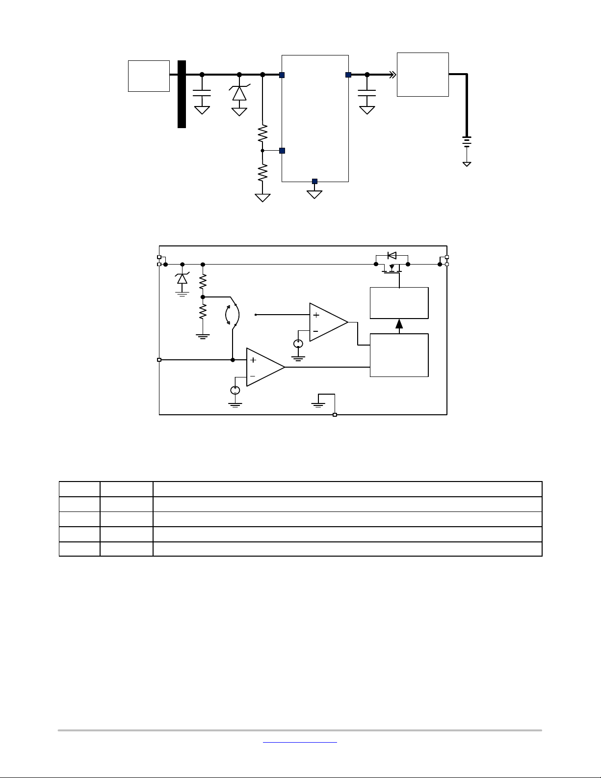
Travel
Adapter
VBUS
1uF
IN
OUT
HV Battery
Charger
1uF
FPF2286
R2
R1
OVLO
GND
Gate Drive
1.2V
Control
Legacy USB /
USB Type C connector
Figure 1. Application Schematic − Adjustable Option
IN OUT
OVLO
0.3V
GND
Figure 2. Simplified Block Diagram
Table 1. PIN FUNCTION DESCRIPTION
Pin No. Pin Name Description
A2, B2 IN Power Input: Switch Input and Device Supply
A1, B1 OUT Power Output: Switch Output to Load
C2 OVLO OVLO Input: Over Voltage Lockout Adjustment Input
C1 GND Ground
www.onsemi.com
2
Page 3
FPF2286UCX
Table 2. MAXIMUM RATINGS
Rating Symbol Value Unit
Input Voltage Range (Note 1) V
Output Voltage Range V
Adjustable Input Range V
Internal FET continuous current I
Maximum Junction Temperature T
Storage Temperature Range T
ESD Capability, Human Body Model (Note 2) ESD
ESD Capability, Charged Device Model (Note 2) ESD
Lead Temperature Soldering
Reflow (SMD Styles Only), Pb−Free Versions (Note 3)
in
out
OVLO
OUT
J(max)
STG
HBM
CDM
T
SLD
Stresses exceeding those listed in the Maximum Ratings table may damage the device. If any of these limits are exceeded, device functionality
should not be assumed, damage may occur and reliability may be affected.
1. Refer to ELECTRICAL CHARACTERISTICS, RECOMMENDED OPERATING RANGES and/or APPLICATION INFORMATION for Safe
Operating parameters.
2. This device series incorporates ESD protection and is tested by the following methods:
ESD Human Body Model tested per AEC−Q100−002 (EIA/JESD22−A114)
ESD Charged Device Model tested per AEC−Q100−011 (EIA/JESD22−C101)
Latch−up Current Maximum Rating: ≤150 mA per JEDEC standard: JESD78
3. For information, please refer to our Soldering and Mounting Techniques Reference Manual, SOLDERRM/D.
−0.3 to 28 V
−0.3 to (Vin + 0.3) V
−0.3 to 23 V
0 to 4 A
150 °C
−65 to 150 °C
2 kV
1 kV
260 °C
Table 3. THERMAL CHARACTERISTICS
Rating Symbol Value Unit
Thermal Characteristics, WLCSP−6 (Note 4)
Thermal Resistance, Junction−to−Air (Note 5)
R
θJA
121.7 °C/W
4. Refer to ELECTRICAL CHARACTERISTICS, RECOMMENDED OPERATING RANGES and/or APPLICATION INFORMATION for Safe
Operating parameters.
5. Values based on 2S2P JEDEC std. PCB.
Table 4. RECOMMENDED OPERATING RANGES
Rating Symbol Min Max Unit
Supply Voltage on VIN V
I/O pins V
Output Current I
IN Capacitor C
OUT Capacitor C
Ambient Temperature T
in
OVLO
out
in
out
A
Functional operation above the stresses listed in the Recommended Operating Ranges is not implied. Extended exposure to stresses beyond
the Recommended Operating Ranges limits may affect device reliability.
2.8 23 V
0 5.5 V
0 3.5 A
0.1
0.1
mF
mF
−40 85 °C
www.onsemi.com
3
Page 4

FPF2286UCX
Table 5. ELECTRICAL CHARACTERISTICS
VIN = 2.8 to 23 V, CIN = 0.1 mF, C
min/max values T
= −40°C to 85°C; unless otherwise noted. (Note 6)
A
Parameter
LEAKAGE AND QUIESCENT CURRENTS
Input Quiescent Current on VIN
Supply Current during Over Voltage VIN = 23 V, V
OVLO Input Leakage Current V
OVER VOLTAGE AND UNDER VOLTAGE LOCKOUT
Under−Voltage Rising Trip Level for VIN
Under−Voltage Falling Trip Level for VIN VIN falling, TA = −40 to 85°C V
Default Over−Voltage Trip Level VIN rising, TA = −40 to 85°C V
OVLO set threshold V
OVLO threshold hysteresis V
Adjustable OVLO range OV_MODE = 0, V
I/O THRESHOLDS
OVLO Input Threshold Voltage
Voltage Increasing, Logic High
Voltage Decreasing, Logic Low
RESISTANCE
On−resistance of Power FET
TIMING
De−bounce Time of Power FET turned on Time from 2.5 V < VIN < V
Switch Turn−On rising Time (Note 8)
Switch Turn−Off Time (Note 8)
THERMAL SHUTDOWN
Thermal Shutdown Temperature (Note 8)
Thermal Shutdown Hysteresis (Note 8) T
Product parametric performance is indicated in the Electrical Characteristics for the listed test conditions, unless otherwise noted. Product
performance may not be indicated by the Electrical Characteristics if operated under different conditions.
6. Performance guaranteed over the indicated operating temperature range by design and/or characterization tested at T
duty cycle pulse techniques are used during testing to maintain the junction temperature as close to ambient as possible.
7. Refer to the APPLICATION INFORMATION section.
8. Values based on design and/or characterization.
9. Depends on the capacitance on OVLO pin.
= 0.1 mF, TA = −40 to 85°C; For typical values VIN = 5.0 V, IIN v 3 A, CIN = 0.1 mF, TA = 25°C, for
OUT
Test Conditions Symbol Min Typ Max Unit
VIN = 5 V, V
VIN = 20 V, V
= V
OVLO
= 0.6 V
OVLO
= 0.6 V 200
OVLO
OVLO
OVLO_TH
= 3.0 V, V
= 0 V I
OUT
VIN rising, TA = −40 to 85°C V
= 1.1 V to 1.3 V, the voltage of
OVLO
OVLO to trigger Over Voltage condition
> 0.5 V V
OVLO
High
Low
VIN = 5 V, I
V
= 0.1 × V
OUT
= 500 mA, TA = 25°C r
OUT
to
IN
IN_OVLO
VIN = 5 V, RL = 100 W, CL = 22 mF,
V
from 0.1 × VIN to 0.9 × V
OUT
IN
I
Q
IN_Q
I
OVLO
IN_UV_R
IN_UV_F
IN_OVLO
V
OVLO_TH
HYS_OVLO
OV_RNG
V
IH_OVLO
V
IL_OVLO
ON
t
SW_DEB
t
R
85 mA
215
−100 100 nA
2.3 2.5 2.7 V
2.4 V
6.6 6.8 7.0 V
1.16 1.19 1.22 V
2 %
4 23 V
0.3
−
−
−
25 35
15 ms
1 ms
RL = 10 W, CL = 0 mF, time from VIN >
V
to V
OVLO
Internal OVP level
External OVP level (Note 9)
OUT
= 0.9 × V
IN
40
100
T
SD
SH
− 130 − °C
− 20 − °C
= TA = 25°C. Low
J
mA
V
−
0.15
mW
ns
www.onsemi.com
4
Page 5

FPF2286UCX
Function Description
General
FPF2286 is an OVP power switch to protect next stage
system which is optimized to lower voltage working
condition. The device includes ultra low on−resistance
power FET (25 mW) and super fast OVP response time
(40 ns).
Power MOSFET
The FPF2286 integrates an N−type MOSFET with 25 mW
resistance. The power FET can work under 2.8 V ~ 23 V and
up to 4 A DC current capability.
Power Supply
The FPF2286 is supplied by IN. IN will be firstly supplied
by OUT when the device is working under USB
On−The−Go (OTG) condition.
Enable Control
There is no specified enable pin for FPF2286. However,
the OVLO can be used as an active LOW enable pin to be
controlled by a GPIO. When OVLO pin is connected to a
high level (higher than 1.2 V), the internal FET will be
turned off. When OVLO pin is connected to 0 V, the FET
will be turned on as long as V
is not higher than 6.8 V.
IN
Under Voltage Lockout
FPF2286 power switch will be turned off when the
voltage on IN is lower than the UVLO threshold V
IN_UV_F
Whenever VIN voltage ramps up to higher than
V
IN_UV_R
after t
Over Voltage Lockout
, the power FET will be turned on automatically
de−bounce time if there is no OV or OT condition.
DEB
The power FET will be turned off whenever VIN voltage
higher than V
IN_OVLO
external resistor ladder or just be default value V
When V
OVLO
decided by default value. When V
V
IH_OVLO
> V
, the power switch will be turned off once V
OVLO_TH
. The external resistor ladder can be decided
. The value of V
is smaller than V
IN_OVLO
IL_OVLO
OVLO
can be set by
IN_OVLO
, V
OVLO
will be
is larger than
OVLO
according to the following equation:
V
IN_OVLO
+ V
OVLO_TH
ǒ1 ) R1ńR2
Ǔ
(eq. 1)
where R1 and R2 are the resistors in Figure 1.
Thermal Shutdown
When the device is in the switch mode, to protect the
device from over temperature, the power switch will be
turned off when the junction temperature exceeds T
SD
. The
switch will be turned on again when temperature drop below
T
− TSH.
SD
.
.
APPLICATIONS INFORMATION
Input Decoupling (Cin)
A ceramic or tantalum at least 0.1 mF capacitor is
recommended and should be connected close to the
FPF2286 package. Higher capacitance and lower ESR will
improve the overall line and load transient response.
Output Decoupling (C
out
)
The FPF2286 is a stable component and does not require
a minimum Equivalent Series Resistance (ESR) for the
output capacitor. The minimum output decoupling value is
0.1 mF and can be augmented to fulfill stringent load
transient requirements.
Thermal Considerations
As power in the FPF2286 increases, it might become
necessary to provide some thermal relief. The maximum
power dissipation supported by the device is dependent
upon board design and layout. Mounting pad configuration
on the PCB, the board material, and the ambient temperature
affect the rate of junction temperature rise for the part. When
ORDERING INFORMATION
Device Default OV Level Marking Package Shipping
FPF2286UCX 6.8 V 3F WLCSP−6L 3000 / Tape & Reel
†For information on tape and reel specifications, including part orientation and tape sizes, please refer to our Tape and Reel Packaging
Specifications Brochure, BRD8011/D
the FPF2286 has good thermal conductivity through the
PCB, the junction temperature will be relatively low with
high power applications. The maximum dissipation the
FPF2286 can handle is given by:
P
D(MAX)
+
ƪ
T
J(MAX)
R
qJA
* T
ƫ
A
(eq. 2)
Since TJ is not recommended to exceed 125°C, then the
FPF2286 soldered on 645 mm
ambient temperature (T
A
2
, 1 oz copper area, and the
) is 25°C. The power dissipated by
the FPF2286 can be calculated from the following
equations:
out
Ǔ
) I
out
@ r
ON
(eq. 3)
Hints
Vin and V
PD[ Vin@ǒIQ@I
printed circuit board traces should be as wide
out
2
as possible. Place external components, especially the input
capacitor and TVS, as close as possible to the FPF2286, and
make traces as short as possible.
†
www.onsemi.com
5
Page 6

MECHANICAL CASE OUTLINE
PACKAGE DIMENSIONS
WLCSP6 1.3x0.9x0.574
CASE 567UV
ISSUE O
DATE 05 JUL 2017
DOCUMENT NUMBER:
DESCRIPTION:
ON Semiconductor and are trademarks of Semiconductor Components Industries, LLC dba ON Semiconductor or its subsidiaries in the United States and/or other countries.
ON Semiconductor reserves the right to make changes without further notice to any products herein. ON Semiconductor makes no warranty, representation or guarantee regarding
the suitability of its products for any particular purpose, nor does ON Semiconductor assume any liability arising out of the application or use of any product or circuit, and specifically
disclaims any and all liability, including without limitation special, consequential or incidental damages. ON Semiconductor does not convey any license under its patent rights nor the
rights of others.
© Semiconductor Components Industries, LLC, 2019
98AON66547G
WLCSP6 1.3x0.9x0.574
Electronic versions are uncontrolled except when accessed directly from the Document Repository.
Printed versions are uncontrolled except when stamped “CONTROLLED COPY” in red.
PAGE 1 OF 1
www.onsemi.com
Page 7

ON Semiconductor and are trademarks of Semiconductor Components Industries, LLC dba ON Semiconductor or its subsidiaries in the United States and/or other countries.
ON Semiconductor owns the rights to a number of patents, trademarks, copyrights, trade secrets, and other intellectual property. A listing of ON Semiconductor’s product/patent
coverage may be accessed at www.onsemi.com/site/pdf/Patent−Marking.pdf
ON Semiconductor makes no warranty, representation or guarantee regarding the suitability of its products for any particular purpose, nor does ON Semiconductor assume any liability
arising out of the application or use of any product or circuit, and specifically disclaims any and all liability, including without limitation special, consequential or incidental damages.
Buyer is responsible for its products and applications using ON Semiconductor products, including compliance with all laws, regulations and safety requirements or standards,
regardless of any support or applications information provided by ON Semiconductor. “Typical” parameters which may be provided in ON Semiconductor data sheets and/or
specifications can and do vary in different applications and actual performance may vary over time. All operating parameters, including “Typicals” must be validated for each customer
application by customer’s technical experts. ON Semiconductor does not convey any license under its patent rights nor the rights of others. ON Semiconductor products are not
designed, intended, or authorized for use as a critical component in life support systems or any FDA Class 3 medical devices or medical devices with a same or similar classification
in a foreign jurisdiction or any devices intended for implantation in the human body. Should Buyer purchase or use ON Semiconductor products for any such unintended or unauthorized
application, Buyer shall indemnify and hold ON Semiconductor and its officers, employees, subsidiaries, affiliates, and distributors harmless against all claims, costs, damages, and
expenses, and reasonable attorney fees arising out of, directly or indirectly, any claim of personal injury or death associated with such unintended or unauthorized use, even if such
claim alleges that ON Semiconductor was negligent regarding the design or manufacture of the part. ON Semiconductor is an Equal Opportunity/Affirmative Action Employer. This
literature is subject to all applicable copyright laws and is not for resale in any manner.
. ON Semiconductor reserves the right to make changes without further notice to any products herein.
PUBLICATION ORDERING INFORMATION
LITERATURE FULFILLMENT:
Email Requests to: orderlit@onsemi.com
ON Semiconductor Website: www.onsemi.com
TECHNICAL SUPPORT
North American Technical Support:
Voice Mail: 1 800−282−9855 Toll Free USA/Canada
Phone: 011 421 33 790 2910
Europe, Middle East and Africa Technical Support:
Phone: 00421 33 790 2910
For additional information, please contact your local Sales Representative
◊
www.onsemi.com
1
 Loading...