

ON Semiconductor Fairchild FAN302HL, Fairchild FAN302UL Design Manualline

Is Now Part of
To learn more about ON Semiconductor, please visit our website at
www.onsemi.com
ON Semi conductor an d the ON Semico nductor logo a re trademar ks of Semicon ductor Comp onents Indus tries, L LC dba ON Semico nductor or it s subsidiari es in the United S tates and /or other coun tries. ON Se miconducto r owns the righ ts to a number
of patents, trademarks, copyrights, trade secrets, and other intellectual property. A listing of ON Semiconductor’s product/patent coverage may be accessed at www.onsemi.com/site/pdf/Patent-Marking.pdf. ON Semiconductor reserve s the right
to make changes without f urther noti ce to any produc ts herein. ON S emicon ductor makes no warran ty, representat ion or guar antee regar ding the suitability of its pro ducts for any partic ular purpose, n or does ON Semic onductor as sume any liabilit y
arisin g out of the applica tion or us e of any product o r circui t, and specific ally dis claims any and all lia bilit y, includin g witho ut limit ation sp ecial, c onsequential or incidental da mages . Buye r is responsib le for it s products and a pplica tions us ing ON
Semic onductor pr oducts, inc luding complia nce with all law s, regulati ons and safet y requirem ents or stan dards, rega rdless of an y support or ap plications in formation p rovided by ON S emiconduc tor. “Typical ” parameter s which may be pr ovided in ON
Semic onductor data s heet s and/or s pecificatio ns can and do vary in diff erent a pplica tions an d actual perf ormance may var y over time. All o perat ing parameter s, including “Typical s” must b e validated for e ach cus tomer ap plicat ion by customer’s
techni cal exper ts. ON Semic onductor do es not conve y any license un der its pate nt rights no r the rights o f others. ON S emiconduc tor produc ts are not des igned, inte nded, or autho rized for use a s a critical c omponent in lif e support s ystems or an y FDA
Clas s 3 medical devi ces or medica l devices wit h a same or similar c lassificat ion in a foreign j urisdictio n or any device s intended for im plantation in t he human body. Sho uld Buyer pur chase or use ON S emiconduct or products f or any such unint ended
or unaut horized appli cation, Buy er shall indemn ify and hold O N Semiconduc tor and its of ficers, e mployees , subsidiari es, affilia tes, and dis tributor s harmless ag ainst all claim s, costs , damages, an d expenses , and reason able attorn ey fees aris ing out
of, dire ctly or indire ctly, any claim o f personal inj ury or death as sociated w ith such unint ended or unauth orized use, e ven if such claim a lleges that ON S emiconduc tor was neglig ent regardin g the design or ma nufacture o f the part. ON S emiconduct or
is an Equa l Oppor tunity/Affirm ative Action E mployer. This li terature is s ubject to all applicable c opyright la ws and is no t for resale in any manner.

www.fairchildsemi.com
AN-6094
Design Guideline for Flyback Charger Using FAN302HL/UL
1. Introduction
More than half of the external power supplies produced
are used for portable electronics such as laptops, cellular
phones, and MP3 players that require constant output
voltage and current regulation for battery charging. For
applications requiring precise Constant Current (CC)
regulation, current sensing in the secondary side is always
necessary, which results in sensing loss. For power
supply designers faced with stringent energy-efficiency
regulations, output current sensing is a design challenge.
The advanced PWM controller FAN302HL/UL can
alleviate the burden of meeting international energy
efficiency regulations in charger designs. The
FAN302HL/UL family uses a proprietary primary-side
regulation (PSR) technique where the output current is
precisely estimated with only the information in the
primary side of the transformer and controlled with an
internal compensation circuit. This removes the output
DL2
+
V
DL
R
HV
AC Line
Fuse
Bridge
L
F
C
DL1
R
C
GATE
current sensing loss and eliminates all external currentcontrol circuitry, facilitating a higher efficiency power
supply design without incurring additional costs. A
Green-Mode function with an extremely low operating
current (200 µA) in Burst Mode maximizes the light-load
efficiency, enabling conformance to worldwide Standby
Mode efficiency guidelines.
This application note presents practical design
considerations for flyback battery chargers employing the
FAN302HL/UL. It includes instructions for designing the
transformer and output filter, selecting the components,
and implementing Constant Current (CC) / Constant
Voltage (CV) control. The design procedure is verified
through an experimental prototype converter using
FAN302UL. Figure 1 shows a typical application circuit
of a flyback converter using the FAN302HL/UL.
R
C
C
R
CL
CL
D
CL
N
N
S
P
SNB
SNB
L
O
D
R
C
O1
R
Bias
C
V
O
I
O
O2
D
A
R
N
A
R
VS1
R
VS2
VDD
C
DD
C
VS
FAN302HL/UL
CS
1
2
GATE
3
VDD
4 5
VS
HV
NC
FB
GND
8
7
6
C
FB
R
BF
R
FR
TL431
R
CS
R
F1
C
FR
R
F2
Figure 1. Typical Application Circuit
AN-6094
P
NIN
P
I
D
I
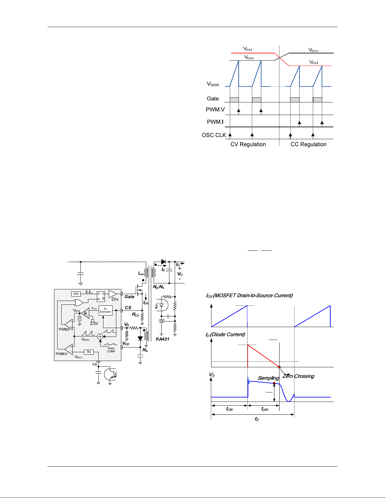
2. Operation Principle
2-1 Constant-Voltage Regulation Operation
Figure 2 shows the internal PWM control circuit of
FAN302. The constant voltage (CV) regulation is
implemented in the same way as the conventional isolated
power supply, where the output voltage is sensed using
voltage divider and compared with the internal 2.5 V
reference of the shut regulator (KA431) to generate a
compensation signal. The compensation signal is
transferred to the primary side using an opto-coupler and
applied to the PWM comparator (PWM.V) through
attenuator Av to determine the duty cycle.
CC regulation is implemented internally without directly
sensing the output current. The output current estimator
reconstructs output current information (V
transformer primary-side current and diode current
discharge time. V
is then compared with a reference
CCR
voltage (2.5 V) by an internal error amplifier and generates
a V
signal to determine the duty cycle.
EA.I
V
and V
EA.I
waveform (V
are compared with an internal sawtooth
EA.V
) by PWM comparators PWM.I and
SAW
PWM.V, respectively, to determine the duty cycle. As seen
in Figure 2, the outputs of two comparators (PWM.I and
PWM.V) are combined with the OR gate and used as a
reset signal of flip-flop to determine the MOSFET turn-off
instant. The lower signal, V
EA.V
and V
duty cycle, as shown in Figure 3. During CV regulation,
determines the duty cycle while V
V
EA.V
HIGH. During CC regulation, V
cycle while V
is saturated to HIGH.
EA.V
determines the duty
EA.I
) using the
CCR
, determines the
EA.I
is saturated to
EA.I
Figure 3. PWM Operation for CC and CV
Output Current Estimation
Figure 4 shows the key waveform of a flyback converter
operating in Discontinuous Conduction Mode (DCM),
where the secondary side diode current reaches zero before
the next switching cycle begins. Since the output current
estimator of FAN302 is designed for DCM operation, the
power stage should be designed such that DCM is
guaranteed for the entire operating range. The output
current is obtained by averaging the triangular output diode
current area over a switching cycle, as calculated by:
t
II I
AVG
== ⋅
OD PK
where I
is the peak value of the primary-side current;
PK
NP and NS are the number of turns of the transformer,
primary side and secondary side, respectively; t
diode current discharge time; and t
N
DIS
P
Nt
SS
2
(1)
is the
is switching period.
s
DIS
K
⋅
PK
S
AVG
I=
O
Figure 2. Internal PWM Control Circuit
N
A
V
⋅
O
N
S
Figure 4. Key Waveforms of DCM Flyback Converter
© 2012 Fairchild Semiconductor Corporation www.fairchildsemi.com
Rev. 1.0.0 • 9/27/12 2

AN-6094
3. Design Consideration
Figure 5. Operation Range of Charger with CC/CV
A battery charger power supply with CC output requires
more design consideration than the conventional power
supply with a fixed output voltage. In CC operation, the
output voltage changes according to the charging
condition of battery. The supply voltage for the PWM
controller (V
auxiliary winding of the transformer, changes with the
output voltage. Thus, the allowable V
determines the output voltage variation range in CC
regulation. FAN302 has a wide supply voltage (V
operation range from 5 V up to 26.5 V, which allows
stable CC regulation even with output voltage lower than
a quarter of its nominal value.
Another important design consideration for CC operation
is that the transformer should be designed to guarantee
DCM operation over the whole operation range since the
output current can be properly estimated only in DCM, as
described in Section 2. As seen in Figure 5, the MOSFET
conduction time (t
decreases in CC Mode, which is proportional to the square
root of the output voltage. Meanwhile, the diode current
discharge time (t
decreases, which is inversely proportional to the output
voltage. Since the increase of t
decrease of t
sum of t
decreases. When the sum of t
switching period, the converter enters CCM. FAN302 has
), which is usually obtained from the
DD
operation range
DD
) decreases as output voltage
ON
) increases as the output voltage
DIS
is dominant over the
ON
DIS
and t
are same as the
DIS
in determining the sum of tON and t
ON
ON
and t
tends to increases as output voltage
DIS
DIS
DD
, the
)
a frequency-reduction function to prevent CCM operation
by extending the switching period as the output voltage
drops, as illustrated in Figure 6. The output voltage is
indirectly sensed by sampling the transformer winding
voltage (V
time, as illustrated in Figure 4. The frequency-reduction
profile is designed such that the on-time remains almost
constant even when the output voltage drops in CC Mode.
) around the end of diode current discharge
SH
f
Δ
S
=
CCG
V
Δ
Figure 6. Frequency Reduction in CC Mode
−
© 2012 Fairchild Semiconductor Corporation www.fairchildsemi.com
Rev. 1.0.0 • 9/27/12 3

AN-6094
4. Design Procedure
In this section, a design procedure is presented using the
Figure 1 as a reference. An offline charger with 6 W / 5 V
output has been selected as a design example. The design
specifications are:
Line Voltage Range: 90~264 V
and 60 Hz
AC
Nominal Output Voltage and Current: 5 V / 1.2 A
Output Voltage Ripple: Less than 100 mV
Minimum Output Voltage in CC Mode: 25% of
Nominal Output (1.25 V)
Maximum Switching Frequency: 140 kHz
Figure 7. Output Voltage and Current Operating Area
[STEP-1] Estimate the Efficiencies
The charger application has output voltage and current
that change over a wide range, as shown in Figure 7,
depending on the charging status of the battery. Thus, the
efficiencies and input powers of various operating
conditions should be specified to optimize the power stage
design. The critical operating points for design:
Estimated primary-side efficiency (E
secondary-side efficiency (E
) for operating point A,
FF.S
) and
FF.P
B, and C. Figure 8 shows the definition of primaryside and secondary-side efficiencies. The primary-side
efficiency is for the power transferred from the AC
line to the transformer primary side. The secondaryside efficiency is for the power transferred from the
transformer primary side to the power supply output.
Since the rectifier diode forward voltage drop does not
change much with its voltage rating, the conduction loss
of output rectifier diode tends to be dominant for a low
output voltage application. Therefore, the distribution of
primary-side and secondary-side efficiencies changes with
the output voltage. With a given transformer efficiency,
the secondary- and primary-side efficiency, ignoring the
diode switching loss, are given as:
N
V
EE
≅⋅
..
FF S FF TX
EEE=
..
FF P FF FF S
where E
FF.TX
0.95~0.98%; V
is the rectifier diode forward-voltage drop.
V
F
O
N
VV
+
OF
/
is transformer efficiency, typically
N
is the nominal output voltage; and
O
(2)
(3)
Table 1. Typical Efficiency of Flyback Converter
Typical Efficiency at Minimum
Output
Line Voltage
Voltage
Universal Input European Input
3.3 ~ 6 V 65 ~ 70% 67 ~ 72%
6 ~ 12 V 70 ~ 77% 72 ~ 79%
12 ~ 24 V 77 ~ 82% 79 ~ 84%
Operating Point A, where the output voltage and
current reach maximum value (nominal output
voltage and current).
Operating Point B, where the frequency drop is
initiated to maintain DCM operation.
Operating Point C, where the output has its
minimum voltage in CC Mode.
Typically, low line is the worst case for the transformer
design since the largest duty cycle occurs at the minimum
input voltage condition. As a first step, the following
parameters should be estimated for low line.
Estimated overall efficiency for operating points A, B,
, E
and C (E
FF@A
FF@B
, and E
conversion efficiency should be estimated to calculate
the input power and maximum DC link voltage ripple.
): The overall power
FF@C
Figure 8. Primary-Side and Secondary-Side Efficiency
With the estimated overall efficiency, the input power at
operating point A is given as:
NN
V
I
OO
=
P
@
IN A
where V
E
N
O
@
FF A
and I
N
are the nominal output voltage and
O
current, respectively.
If no reference data is available, use the typical
efficiencies in Table 1.
© 2012 Fairchild Semiconductor Corporation www.fairchildsemi.com
Rev. 1.0.0 • 9/27/12 4
(4)

AN-6094
The input power of transformer at operating point A is
given as:
NN
I
V
P
.@
IN T A
=
OO
E
.@
FF S A
(5)
To reduce the switching frequency as the output voltage
drops in CC Mode for maintaining DCM operation, the
output voltage needs to be sensed. FAN302 senses the
output voltage indirectly by sampling auxiliary winding
voltage just before the diode conduction finishes, as
explained with Figure 4 in Section 2. Since the switching
frequency starts decreasing as V
sampling voltage drops
S
below 2.15 V, as illustrated in Figure 6, the output voltage
at operating point B can be obtained as:
VVVV
2.15
= ⋅+ −
OB O FSH FSH
@..
V
SH A
@
where V
SH@A
point A, which is typically designed as 2.5 V and V
is the rectifier diode forward voltage drop at the V
N
()
(6)
is the VS sampling voltage at operating
F.SH
S
sampling instant (85% of diode conduction time), which
is typically about 0.1 V. Note that V
third of V
since the Vs voltage sampling occurs when
F
is less than a
F.SH
the diode current is very small.
The overall efficiency at operating point B, where the
frequency reduction starts, can be estimated as:
EE
≅⋅ ⋅
@@
FF B FF A
V
VV
@
OB F
@
OB
+
N
VV
+
OF
N
V
O
(7)
Note that the efficiency changes as the output voltage
drops in CC Mode. The efficiency should be also
estimated for each operating point (B and C).
The secondary-side efficiency at operating point B can be
estimated as:
EE
≅⋅ ⋅
.@ .@
FF S B FF S A
V
@
OB
VV
+
@
OB F
N
VV
+
OF
N
V
O
(8)
Then, the power supply input power and transformer input
power at operating point B are given as:
N
⋅
@
OB O
E
@
FF B
⋅
@
.@
FF S B
N
VI
OB O
E
(9)
(10)
P
IN B
P
.@
IN T B
=
@
=
VI
The overall efficiency at operating point C can be
approximated as:
EE
≅⋅ ⋅
@
FF C FF
where V
VV
OC F
is the minimum output voltage for CC
O@C
V
OC
@
@
+
N
VV
+
OF
N
V
O
(11)
Mode at operating point C.
The secondary-side efficiency at operating point C can be
estimated as:
EE
≅⋅ ⋅
.@ .@
FF S C FF S A
V
@
OC
VV
+
@
OC F
N
VV
+
OF
N
V
O
(12)
Then, the power supply input power and transformer input
power at operating point C are given as:
P
IN C
P
IN T C
@
.@
=
=
VI
OC O
VI
⋅
@
E
@
FF C
⋅
@
OC O
E
.@
FF S C
N
N
(Design Example)
To maximize efficiency, a low-voltage-drop Schottky
diode whose forward voltage drop is 0.35 V is selected.
Assuming the overall efficiency is 73% and the
transformer efficiency is 97% at operating point A
(nominal output voltage and current) for low line, the
secondary-side efficiency is obtained as:
N
V
EE
Then, the input powers of the power supply and
transformer at operating point A are obtained as:
P
IN A
P
IN T A
≅⋅ =
FF S A FF T X
.@ .
NN
V
I
OO
= ==
@
E
@
FF A
NN
VI
.@
OO
E
FF S A
.@
O
N
VV
+
OF
6
8.22
0.73
6
6.62
0.907
0.907
W
W= ==
The efficiencies at operating point B are:
V
@
EE
≅⋅ ⋅ =
@@
FF B FF A
EE
≅⋅ ⋅ =
FF S B FF S A
.@ .@
OB
VVV
+
OB F O
@
V
OB
VVV
@
OB F O
VV
OF
@
+
N
+
0.722
N
N
VV
+
OF
N
0.896
Then, the input powers of the power supply and
transformer at operating point B are obtained as:
N
V
I
OBO
P
IN B
P
IN T B
@
.@
@
= =
E
FF B
@
V
I
OBO
@
= =
E
FF S B
.@
N
7.07
5.69
W
W
The primary-side and secondary-side efficiencies at the
operating point C are calculated as:
V
@
EE
≅⋅ ⋅ =
@@
FF C FF A
EE
≅⋅ ⋅ =
.@ .@
FF S C FF S A
OC
VVV
+
@
OC F O
V
OC
VVV
@
OC F O
N
VV
OF
@
+
+
0.610
N
N
VV
+
OF
N
0.758
Then, the input powers of the power supply and
transformer at operating point C are obtained as:
P
IN C
P
IN T C
@
.@
V
OC O
=
=
I
⋅
@
E
FF C
@
V
⋅
OC O
@
E
FF S C
.@
N
2.46
W
=
N
I
=
1.98
W
(13)
(14)
© 2012 Fairchild Semiconductor Corporation www.fairchildsemi.com
Rev. 1.0.0 • 9/27/12 5

AN-6094
I
I
I
I
P
I
D
R
D
D
[STEP-2] Determine the DC Link Capacitor
(C
) and the DC Link Voltage Range
DL
It is typical to select the DC link capacitor as 2-3 µF per
watt of input power for universal input range (90264 V
input range (195~265 V
chosen, the minimum DC link voltage is obtained as:
The maximum DC link voltage is given as:
The minimum DC link voltage and its ripple change with
input power. The minimum input DC link voltage at
operating point B is given as:
) and 1 µF per watt of input power for European
AC
min min 2
=⋅ −
VV
@
DL A LINE
where V
2( )
min
is the minimum line voltage; CDL is the
LINE
DC link capacitor; f
). With the DC link capacitor
rms
−
(1 )
PD
@
NA ch
⋅
Cf
DL L
is the line frequency; and Dch is
L
(15)
the DC link capacitor charging duty ratio defined as
shown in Figure 9, which is typically about 0.2.
max max
LINE
2
max
is the maximum line voltage.
(16)
VV=⋅
DL LINE
where V
min min 2
VV
DL C LINE
@
2 (90) 117
=⋅ − =
2( )
=⋅ −
2.46(1 0.2)
2
26.8 10 60
−
−
⋅× ⋅
6
[STEP-3] Determine Transformer Turns
Ratio
Figure 10 shows the MOSFET drain-to-source voltage
waveforms. When the MOSFET is turned off, the sum of
the input DC link voltage (V
reflected to the primary side is imposed across the
MOSFET, calculated as:
VVV=+
SDLRO
maxnom
where VRO is reflected output voltage, defined as:
N
p
N
VVV
OOF
where N
()
=+
N
s
and NS are number of turns for the primary
P
side and secondary side, respectively.
DL
(1 )
PD
−
@
NC ch
Cf
⋅
DL L
V
) and the output voltage
(19)
(20)
When the MOSFET is turned on; the output voltage,
(1 )
min min 2
VV
@
DL B LINE
2( )
=⋅ −
PD
−
@
NB ch
Cf
⋅
DL L
(17)
The minimum input DC link voltage at operating point C
is given as:
−
(1 )
PD
@
min min 2
=⋅ −
VV
@
DL C LINE
2( )
NC ch
⋅
Cf
DL L
(18)
together with input voltage reflected to the secondary, are
imposed across the secondary-side rectifier diode
calculated as:
N
maxnom N
VVV
S
=+
DL O
N
P
(21)
As observed in Equations (19), (20), and (21); increasing
the transformer turns ratio (N
/ NS) increases voltage
P
stress on the MOSFET while reducing voltage stress on
the rectifier diode. Therefore, the N
/ NS should be
P
determined by the trade-off between the MOSFET and
diode voltage stresses.
The transformer turns ratio between the auxiliary winding
and the secondary winding (N
/ NS) should be
A
determined by considering the allowable IC supply
voltage (V
condition, as shown in Figure 11, where the minimum
V
Figure 9. DC Link Voltage Waveforms
(Design Example)
By choosing two 6.8 µF capacitors
in parallel for the DC link capacitor, the minimum and
maximum DC link voltages for each condition are
obtained as:
(1 )
min min 2
VV
DL A LINE
@
max
VV=⋅ =
DL
VV
DL B LINE
@
2(90) 96
=⋅ − =
© 2012 Fairchild Semiconductor Corporation www.fairchildsemi.com
Rev. 1.0.0 • 9/27/12 6
2( )
=⋅ −
2
2 (90) 90
=⋅ − =
2 6.8 10 60
2 264 373
min min 2
2( )
=⋅ −
7.07(1 0.2)
2
26.8 10 60
⋅× ⋅
PD
8.22(1 0.2)
−
⋅× ⋅
−
−
6
−
@
IN A ch
Cf
⋅
DL L
−
6
(1 )
D
−
@
NB ch
Cf
⋅
DL L
V
V
typically occurs at minimum load condition. Due to
DD
the voltage overshoot of the auxiliary winding voltage
caused by the transformer leakage inductance; the V
operating point C tends to be higher than the V
minimum load condition.
The V
min
VVVV
DOFFA
where V
auxiliary winding diode.
The transformer turns ratio should be determined such
that V
N
A
()
N
S
Since the V
smaller N
consumption. However, 2~3 V margin (V
) range. The VDD voltage varies with load
DD
at minimum load condition is obtained as:
DD
N
A
≅+−
()
N
S
is the diode forward-voltage drop of the
FA
min
is higher than the VDD UVLO voltage, such as:
DD
VV V V V
+−> +
OF FAUVLO MRGN
min
is related to standby power consumption,
DD
/ NS leads to lower standby power
A
max
MRGN
at
DD
at
DD
(22)
(23)
) should be
 Loading...