

Page 1
NCN5100 Arduinot Shield
Evaluation Board
User's Manual
EVBUM2715/D
INTRODUCTION
KNX [3] is a popular open home and building automation standard
ON Semiconductor has a series of transceivers that handle the low
level communication.
The NCN5100ASGEVB evaluation boards are Arduino-compatible
shields enabling rapid prototyping with a microcontroller of choice.
All external components necessary for operating the transceivers are
present on the shield. Plug it in a Arduino-compatible development kit
and start developing!
FEATURES
• Arduino Uno V3 compatible connectors
♦ Compatible with a wide variety of microcontroller development
boards
• Four on-board buttons/LEDs to build a dimmer application
• Available in UART- and SPI-version
♦ Fully KNX-compliant transceiver
• Easily get started with KNX
• Maximum bus current up to 40 mA
2
• Two high-efficiency DC-DC converters
♦ 3.3 V fixed output
♦ 1.2 V to 21 V variable output
• Integrated 20 V linear regulator output
1
.
www.onsemi.com
EVAL BOARD USER’S MANUAL
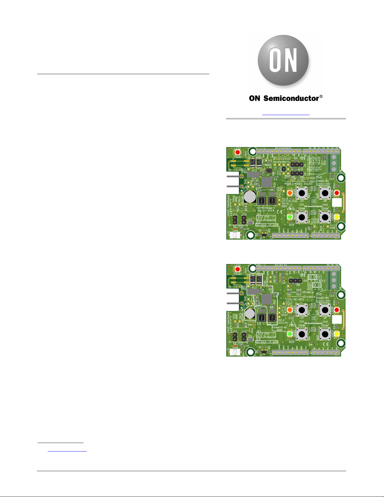
Figure 1. NCN5100AS-1 Evaluation Board
OVERVIEW
The NCN5100ASGEVB boards come in three variants containing
the NCN5110, NCN5121 and NCN5130 transceivers. The NCN5110
is a bit transceiver and all the timings are handled by the
microcontroller. Both the NCN5121 and NCN5130 also implement
the MAC layer, reducing the software development effort. All critical
timings are handled by the transceiver.
All transceivers include two high-effciency DC-DC converters. One
fixed converter generating 3.3 V, supplies the transceiver and other
optional peripherals such as a microcontroller. The second DC-DC
converter has an adjustable output voltage ranging from 1.2 V to 21 V
and can be used to supply peripherals such as, relays, a display, etc. ...
The Arduino shield form factor makes it easy to start developing;
just plug the shield into a compatible microcontroller board and start
coding. Thanks to the on-board buttons and LEDs, it is not necessary
to plug in additional shields to start testing. A simple dimmer
application can be set-up in no time with only the KNX
Arduino-shield.
1
https://my.knx.org
2
For the NCN5130 and NCN5110 version. The NCN5121 goes up to 24 mA.
© Semiconductor Components Industries, LLC, 2020
October, 2020 − Rev. 2
1 Publication Order Number:
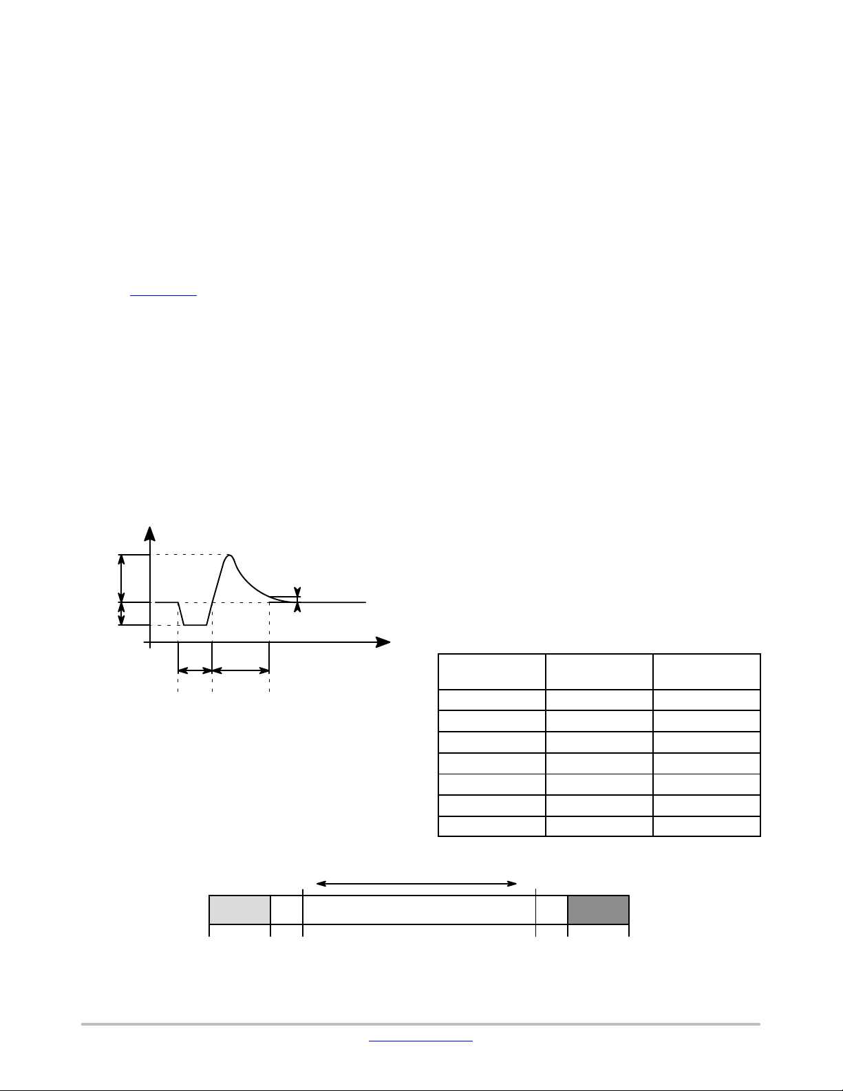
Figure 2. NCN5100AS-2 Evaluation Board
EVBUM2715/D
Page 2
EVBUM2715/D
Both the NCN5121 and NCN5130 come with an SPI and
UART communication interface. The latter is fully
TP-UART compatible, enabling the use of existing
compatible software.
The boards are 2 layer PCB’s with single-sided assembly,
demonstrating that it is possible to easily develop low-cost
applications.
EVALUATION BOARD OVERVIEW
The main connectivity to the evaluation board is provided
through the Arduino V3 headers which can be seen in
Figure 1. This has the advantage that the board is compatible
with a wide variety of microcontroller development boards.
Refer to Appendix C
The KNX-Bus
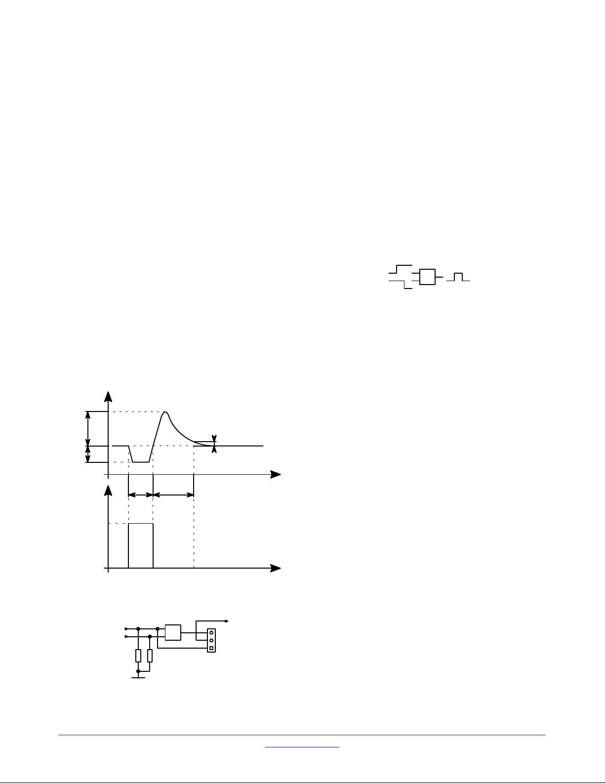
, Table 6 for a list of tested platforms.
The KNX-bus consists of a twisted pair cable providing
both data and power. The voltage on the bus varies between
21 V to 32 V (V
in Figure 3). Communication on the bus
DC
is done at 9600 baud asynchronously. A logic one is
represented by the DC-level on the bus staying constant. For
a logic zero, the bus is pulled 3 V to 10 V below the DC-level
first. This is called the active pulse which has a duration of
typically 35 ms. Following immediately after is the
equalisation pulse. During this time, the voltage can swing
up to 13 V above the DC-level and will decay exponentially
in 69 ms.
V
BUS
V
eq
V
end
V
act
V
DC
Fan-in
Every device connected to the KNX-bus will draw current
from the bus to supply the application. The KNX standard
specifies the current should be limited to the real need. For
every KNX-device the maximum current draw is specified
in its datasheet according to the fan-in-model [1]. The
fan-in-model is used to determine how many devices can be
connected to one physical segment of the bus. All the
ON Semiconductor KNX transceivers contain a built-in
mechanism to keep the draw within the value specified in its
datasheet. This makes sure that the device complies with the
standard.
The fan-in pin sets the maximum current drawn from the
bus. The transceiver will actively keep the current below the
set limit.
Both transceivers (NCN5121 and NCN5130) have two
pre-defined fan-in modes. These can be selected by either
connecting the fan-in pin to GND or leaving it floating.
Leaving it floating, the maximum bus current is limited to
10 mA. Tied to GND the limit is set to 20 mA.
The NCN5130 also offers an external fan-in mode. In this
mode the current limit can be set linearly from 5 mA to
40 mA. This is achieved by connecting a resistor with
a value of 10 kW to 93.1 kW to the fan-in pin. The
fan-in-model [1] specifies discrete current classes. When
designing the application and defining the current
consumption, the next higher value of one of the classes
must be selected. According to section 3.3 of the KNX test
specification [2] the maximum allowed bus current
consumption for a fan-in-model of 10 mA is 12 mA. For
other fan-in models it is allowed to scale this value
accordingly. For example, a 20 mA fan-in-model allows to
draw 24 mA from the bus.
Active
Equalisation
pulse
35 ms
pulse
69 ms
Figure 3. Waveform Seen on the Bus when
Transmitting a Logical Zero
Figure 3 shows a typical waveform on the bus
representing a logical zero.
2 k
40 mA
10 k
Figure 4. The Different Fan-in Settings
www.onsemi.com
20 mA 10 mA
Pre-defined
fan-in
R
3
0
t
Linear range
External fan-in
Only for NCN5130
Table 1. RECOMMENDED FAN-IN RESISTOR VALUES
1. According to the fan-in-model [1].
2
I
bus,lim
R
3
∞ 11.4 mA 10 mA
0 W
10 kW
13.3 kW
20 kW
42.2 kW
93.1 kW
(Typical Values)
5 mA
250 k93.1 k
22.3 mA 20 mA
43.9 mA 40 mA
33.0 mA 30 mA
22.1 mA 20 mA
10.7 mA 10 mA
5.1 mA 5 mA
Pre-defined
fan-in
∞
Current Class
(Note 1)
Page 3
EVBUM2715/D
A list of recommended fan-in resistor values can be found
in Table 1. For the listed resistor values, the corresponding
current limits are specified in the datasheet.
If a resistor value is used, other than the ones specified in
Table 1, the following formula can be used to calculate the
corresponding bus current limit:
Buffer Capacitor
I
bus,lim
+ 4 10*4)
434
R
A
3
(eq. 1)
Besides the maximum allowed current drawn from the
bus, the KNX standard also specifies at which rate the bus
current is allowed to change. This requirement introduces
the need for a large buffer capacitor. When the load current
changes abruptly this capacitor must deliver the required
energy. The KNX-transceiver will charge the capacitor
again after the load step using a fixed current slope.
According to the KNX test specification [2] a device with
a fan-in-model of 10 mA is allowed to change its current
draw from the bus with a slope of 0.5 mA/ms. Section 3.3
specifies that this can be increased accordingly with the
fan-in-model. The following formula can be used to
calculate the allowed bus current slope:
DI
bus
+ 0.05ńms @ I
Dt
fan−in−model
(eq. 2)
The datasheet (pages 18−19) of the NCN5121/NCN5130
describes how to dimension the buffer capacitor. The KNX
Family Efficiency Calculator
3
is a tool developed to help
customers with this dimensioning.
Common Mode Choke
If desired optionally a common mode choke such as the
Murata 50475C can be mounted on the footprint of L1. This
helps to block common mode disturbances, but in most
applications, this is not required.
Before soldering the choke on the foreseen footprint of
L1, the tracks shorting the component must be cut.
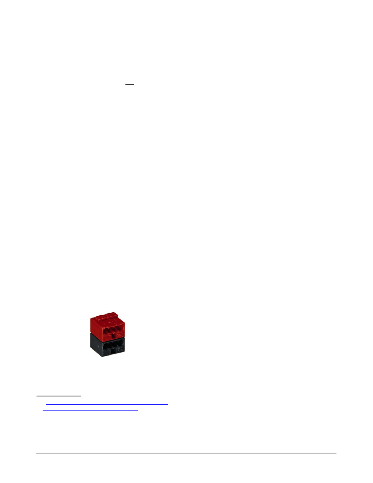
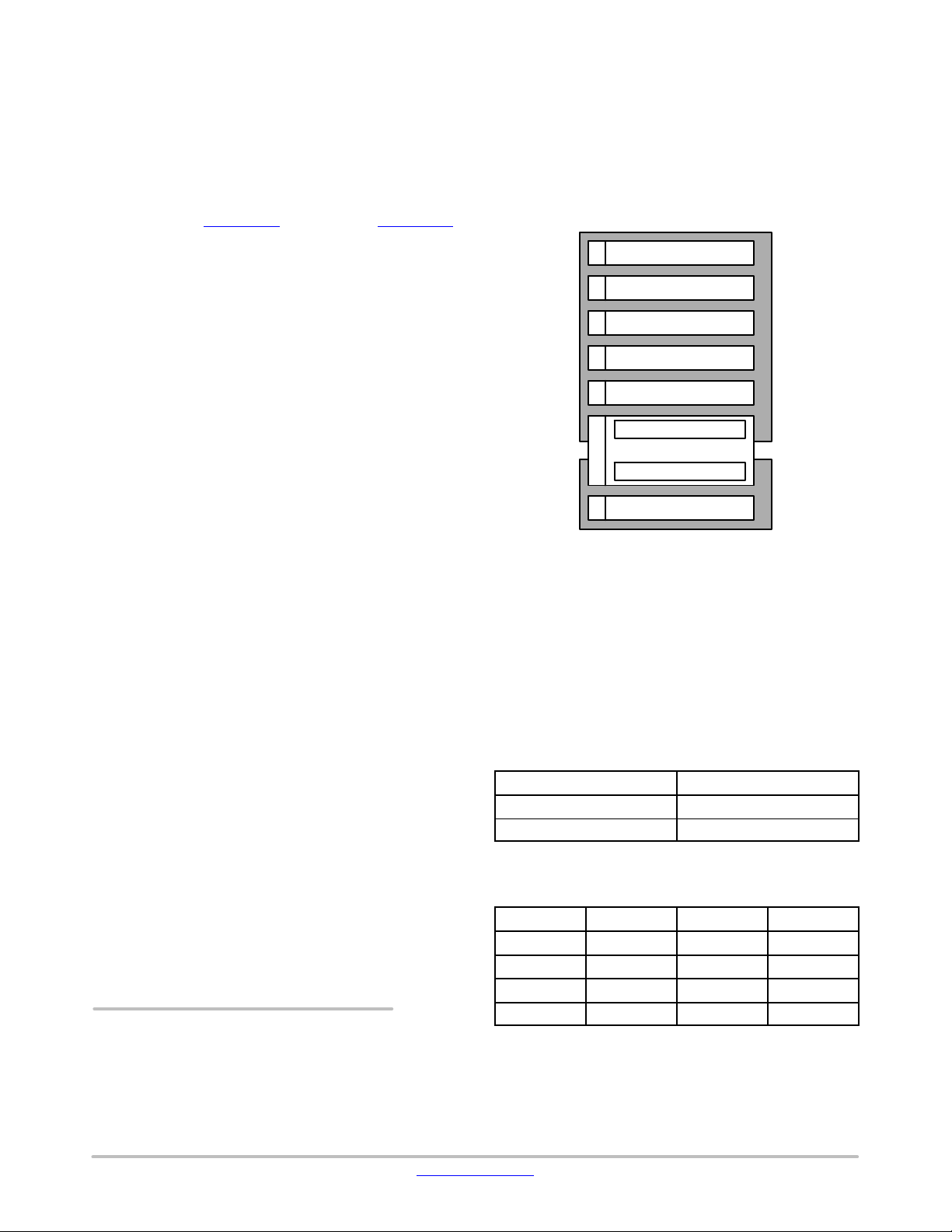
Figure 5. Wago 243−211 Terminal Block
3
https://www.onsemi.com/pub/Collateral/KNX%20FAMILY
%20EFFICIENCY%20CALCULATOR.XLSM
Power
The board is powered through the KNX-connector. These
two pins (KNX+/KNX- in Figure 9) mate with a typical
KNX terminal block such as the Wago 243−211, illustrated
in Figure 5. No additional connection is required as the
board will generate its own supply voltages. An input
voltage up to 30 V is tolerated. Using a standard KNX power
supply is the safest option as it generates the correct voltage
and has a built-in protection.
It is possible to use a laboratory supply, but be sure to
correctly set the output voltage to avoid damaging the board.
By using a laboratory power supply, it is not possible to send
messages on the KNX-bus. To enable communication on the
bus, a special choke must be placed between power supply
and development board. An example of such a choke is the
Siemens GAMMA Choke N 120/02.
To power the microcontroller development board there
are several options.
• Most modern microcontroller development boards can be
supplied through the 3V3-pin, this eliminates the need for
additional LDO’s, and lowers the overall power
consumption.
On the shield, there is always a 3.3 V supply present,
which is also used to supply the KNX transceiver. This
supply voltage can be routed to the 3V3-pin on the
Arduino headers by shorting J11 (Figure 6).
• Arduino-compatible development boards typically
accept a supply voltage of 7 V to 12 V, either through the
on-board DC-jack (if present) or the VIN-pin on the
headers.
The shield can supply the microcontroller through the
VIN-pin. When J10 is shorted (see Figure 6), the 9 V
generated by DC-DC2 is routed to the VIN-pin. In this
configuration, the whole system is supplied through the
KNX-bus and no additional power supplies are required.
• The microcontroller development board may be supplied
through an external supply. This occurs when debugging
the board through USB with the KNX-connector
disconnected. In this case remove both J10 and J11
(Figure 6).
Debugging
During the development of the application code it is very
likely the microcontroller development board is powered
through the USB connection with the PC while debugging.
This introduces the risk that the KNX-transceiver is
powered through the reset line. Current can flow from the
NRST-output of the debugger into the RESETB-pin of the
transceiver through the internal ESD diodes as shown in
Figure 7. As a result, the NRST-line might be pulled low,
resetting the microcontroller. This makes it impossible to
debug the application.
www.onsemi.com
3
Page 4
EVBUM2715/D
To avoid this situation a transistor is added in series with
the NRST-line as shown in Figure 8. If the 3.3 V from the
KNX transceiver is absent, the transistor does not conduct,
and prevents current flow into the RESETB-pin. However,
if the 3.3 V supply is present, it is still possible for the KNX
transceiver to pull the NRST-line low. It is not necessary to
use this circuitry in the end application. In almost all
applications, the microcontroller will be powered from
the transceiver’s supply, and this situation will never
occur.
KNX power supplies are isolated. This means that the
KNX-ground is not connected to earth. On most
microcontroller development boards the ground connection
on the Arduino headers is connected to USB ground. The
USB ground on a PC is always connected to the earth
potential. So when connecting the development board to the
PC the KNX-ground is connected to the earth potential. This
might lead to the “pick-up” of interferences leading to
communication errors. To avoid these it is a good practice to
use an USB-isolator, such as the Olimex USB-ISO.
J11
J10
3V3 from DC−DC1 to 3V3
on the Arduino headers
NCN5100 evaluation board
KNX
DC−DC1
3.3 V
Powering External Circuitry
The transceiver’s 20 V LDO and DC-DC2 converter can
be used to power additional circuitry, e.g. a relay. When
additional shields are stacked, which take their power from
the VIN-pin, these can be powered by connecting DC-DC2
to the VIN-pin. This can easily be done by placing J10 as
shown in Figure 6.
If the additional circuitry is not a shield or if the shield is
powered in another way, the three pin screw terminal can be
used. Figure 9 shows the pin-out of this connector. It is also
possible to power additional circuitry using DC-DC1. This
converter delivers a fixed 3.3 V with a maximal output
current of 100 mA, ideal to supply, for example,
a microcontroller.
Arduino
3V3
NCN5100 evaluation board
KNX
NCN5100 evaluation board
KNX
DC−DC2
20 V LDO
DC−DC1
DC−DC2
20 V LDO
DC−DC1
DC−DC2
20 V LDO
1.2 to 21 V
20 V
J11
3.3 V
1.2 to 21 V
20 V
J11
3.3 V
1.2 to 21 V
20 V
VIN
USB 5 V
J10
9V from DC−DC2 to VIN
Arduino
3V3
VIN
USB 5 V
J10
Arduino motherboard
supplied externally
Arduino
3V3
VIN
USB 5 V
5 V LDO 3.3 V LDO MCU (3.3 V)
5 V LDO 3.3 V LDO MCU (3.3 V)
5 V LDO 3.3 V LDO MCU (3.3 V)
USB from PC
Figure 6. Jumper Settings for the Three Possible Supply Configurations
www.onsemi.com
4
Page 5
EVBUM2715/D
Arduino
Debugger
NCN5100 evalutation board
Vdd
NRST
RESETB
3V3
NCN5100
Figure 7. The Internal ESD Diodes Pulling the
NRST-line Low
NRST
3V3
Or use the KNX Family Efficiency Calculator
4
which can
be found on the ON Semiconductor website.
Inputs and Outputs
Arduino Header Pin-Out
Most of the buttons and LEDs are connected to digital pins
on the Arduino headers. Two of the buttons and one LED are
connected to analog input pins. This was done to keep the
2
I
C-pins free for other purposes. The same applies for the
TREQ-pin.
The SAVEB-pin is connected to a digital pin which has
interrupt capabilities. This is necessary to provide a signal
to the microcontroller as fast as possible indicating the bus
voltage is dropping.
All the LEDs are connected to PWM-capable pins,
allowing the application to dim the LEDs if desired.
A complete net list for the microcontroller connections is
given in Appendix A
, Table 4 and in Appendix B, Table 5.
NCN5110
RXD1
RXD2
SPI_MISO
SPI_MOSI
SPI_SCK
SPI_CS
SW3
LED4
SW3
LED4
SW1
SW1
LED2
LED2
SW4
LED3
SW4
LED3
SAVEB
LED5
SAVEB
LED5
TX
TX
RX
RX
NCN5121
NCN5130
R
1
560 W
Q
1
R
2
10 kW
RESETB
3V3
NCN5100
Figure 8. The Transistor Q1, Prevents Current Flow
when the 3.3 V is Not Present
Adjusting the DC-DC2 Output Voltage
DC-DC2 is adjustable and can be configured to generate
a voltage between 1.2 V to 21 V. This enables supplying
a very wide range of applications. By default, the output
voltage is set to 9 V. This makes it suitable to supply an
Arduino-compatible development board, which typically
accepts an input range of 7 V to 12 V.
To adjust the output voltage the values of the feedback
resistors must be changed. These are located at the bottom
left corner of the PCB, making them easily resolderable. The
required resistor values can be calculated from:
* 1.2
V
R18+ R22@
VDD2
1.2
(eq. 3)
AVDD
GND
D13
D12
D11
D10D9D8D7D6D5D4D3D2D1D0
CH1 CH2
SW3 SW4
LED4
SW1 SW2
LED2
GND
GND
VIN
A0
ANAOUT
TXD
NRST
IOREF
RESETB
RESETB
3V3
5V
A2
A1
SW2
TREQ
SW2
LED5
LED3
A3
A4
S1
LED6
S1
LED6
LED1
Power
KNX*
KNX+
XCLK
8 MHz / 16 MHz
Programming
button/LED
LED6
S1
D15
D14
Figure 9. Evaluation Board Connectivity
(KNX-Shield)
4
https://www.onsemi.com/pub/Collateral/KNX%20FAMILY
%20EFFICIENCY%20CALCULATOR.XLSM
Arduino
GND
9V
20V
Arduino
A5
NCN5121
NCN5130
NCN5110
www.onsemi.com
5
Page 6
EVBUM2715/D
User Buttons and LEDs
The shield has 4 on-board push buttons (SW1...4) and
4 LEDs (LED2...5) to enable the development of switching
apps in particular. For a dimmer application the four buttons
are split into two groups marked on the PCB as channel1 and
channel2 (CH1/CH2). The upper button in the channel is
used to dim up, whilst the other one is used for dimming
down. Refer to Appendix A
, Table 4 and Appendix B,
Table 5 to see how these are connected to the I/O pins of the
microcontroller.
It is possible to stack other shields containing I/Os which
are used for the end application. Remove R26−R29 and
R33−R36 if the buttons or LEDs conflict with the pin-out of
the other shields used.
Programming Push Button and LED
To assign an individual address to a device in
a KNX-network, the device must be put into programming
mode. The simplest way to do this is by pressing the
programming button (S1). LED6 indicates if the device is in
programming mode.
It is possible to customize the entering in programming
mode e.g. pushing two buttons simultaneously.
Microcontroller Clocking
NCN5130 and NCN5121 have the capability to deliver
a clock signal to the microcontroller. This clock signal is
available on the XCLK-pin of the transceiver and routed to
a 2.54 mm header pin on the shield (See Figure 9). Because
the Arduino headers do not foresee a dedicated pin to pass
clock signals, it is mandatory to route this signal manually
to the microcontroller. This is only necessary if it is desired
to use this signal to clock the microcontroller. In most cases
the microcontroller will be clocked from its internal
RC-oscillator or from an external crystal.
By default, the clock signal on the XCLK-pin is 16 MHz.
It can be changed to 8 MHz by tying the XSEL-pin to
ground: De-solder R23 and solder a 0 W resistor on the pads
of R30.
Digital Communication Interface
Both the NCN5121 and NCN5130 implement the mac
layer of the OSI model as shown in Figure 10. They will
handle the coding and decoding of messages, sending
acknowledges, etc... Critical low level timings such as the
duration of the active pulse are all managed by the
transceiver. The transceiver makes sure that the collision
avoidance
5
is handled correctly without any intervention by
the host controller. This greatly reduces the software
development effort. To communicate with the mac layer
both a UART- and SPI-interface are supported. Note that
5
CSMA/CA: Carrier-sense multiple access with collision
avoidance.
when the transceiver operates in SPI-mode it acts as the
master. The microcontroller must support slave mode in
order to be able to communicate with the transceiver. To
select in which mode the KNX-transceiver operates (UART
or SPI) the MODE2-pin is used. When tied to GND using
R32, the transceiver operates in UART-mode. Tying it to
V
using R25 puts the transceiver in SPI-mode.
DD1
7
6
5
4
3
2
1
Figure 10. Placement of the Transceivers
Application layer
Presentation layer
Session layer
Transport layer
Network layer
Logic link control
Data link layer
Media access control
Physical layer
in the OSI Model
Host controllerNCN5121/30
560 W resistors protect the I/O lines going to the
microcontroller. Depending on which resistors are mounted
either the UART or the SPI-lines are connected. If desired it
is possible to transform a UART shield into SPI and vice
versa by soldering/de-soldering the resistors as listed in
Table 2.
Table 2. COMMUNICATION INTERFACE RESISTOR
MOUNTING OPTIONS
Communication Interface Resistor Mounted
UART R16, R17, R32
SPI R9, R11, R12, R13, R15, R25
Table 3. SELECT THE RIGHT BAUD RATE USING
J1/J2
J2 J1 Parity Bit Baud Rate
0 0 even 19 200 bps
0 1 even 38 400 bps
1 0 none 19 200 bps
1 1 none 38 400 bps
www.onsemi.com
6
Page 7
EVBUM2715/D
Selecting The Baud Rate
Jumpers J1 and J2 allow easy configuration of the baud
rate and parity. This is only used in UART-mode. In
SPI-mode, the communication speed is fixed to 500 kbps.
To make the UART-communication more robust, it is
possible to enable the transmission of an even parity bit with
every data byte. For the complete settings refer to the
silkscreen on the shield or to Table 3.
Analog Communication Interface
The NCN5110 transceiver doesn’t contain any digital
functionality, implementing only the physical layer of the
OSI model. Both the TXD- and RXD-lines are directly
connected to the KNX-transmitter/receiver.
Pulling the TXD high will make the transceiver drop the
bus voltage as shown in Figure 11. Once the transmit line is
pulled low again, the transceiver will put an equalisation
pulse on the bus. The duration the bus voltage stays by an
amount of V
below VDC, is determined by the
act
microcontroller. As a consequence the microcontroller is
also responsible for collision detection and avoidance. As
well as the encoding and decoding of messages, sending
acknowledges, etc... must be implemented in the
microcontroller, increasing the software complexity.
The RXD-line will become high when an active pulse is
detected on the bus. As the transceiver also receives the data
itself transmitted on the bus, this line will also become high
during transmission.
V
BUS
V
eq
V
end
V
act
Active
Equalisation
pulse
TXD
&
D12
D11
pulse
35 ms 69 ms
TXD/RXD
[V]
3.3
0
Figure 11. Communication with the NCN5110 and the
Corresponding Levels on the KNX-Bus
V
DC
t
t
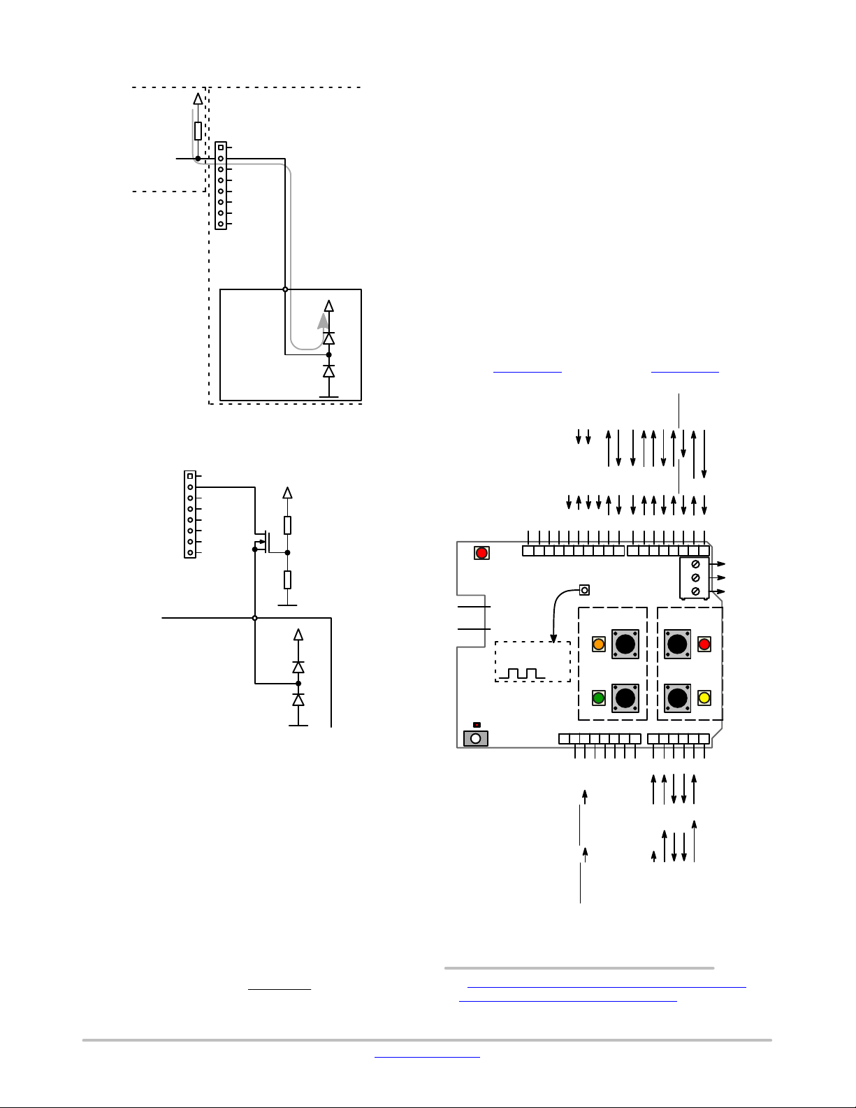
Enable Interface
The timing of the pulses which drive the NCN5110 are
extremely time critical. Some microcontroller families have
special timer modes which can be used to generate the
correct pulses. Using these modes, would limit the use of the
software to a certain microcontroller family.
An AND port combines the signals coming from D11 and
D12. The schematic is shown in Figure 12. It provides
a mechanism to set and clear the transmit signal, without the
use of special timers only available in specific
microcontroller families.
Two timers can be used, one to generate a rising edge, the
other to generate a falling edge. Both signals are combined
to create the desired transmit signal as shown in Figure 13.
Both input pins of the AND port are pulled low. This
ensures that during the startup of the microcontroller, the
transceiver won’t transmit.
&
Figure 13. Combination of a Rising and Falling Edge
to Create the Transmit Signal
PCB LAYOUT GUIDELINES
When designing a PCB for the KNX-transceiver it is
important to take certain layout aspects into consideration.
The following good practices will help to improve the EMC
performance of the whole application. The Arduino shield
is a two-layer PCB, with the main ground plane on the
bottom layer. Empty space on the top layer is filled in with
ground copper, but this is not a ground plane.
DC-DC Converters
Electromagnetic interference is dominated by the DC-DC
converters. These converters switch at frequencies around
300 kHz. Without due consideration for PCB layout,
radiated emissions can become a serious issue.
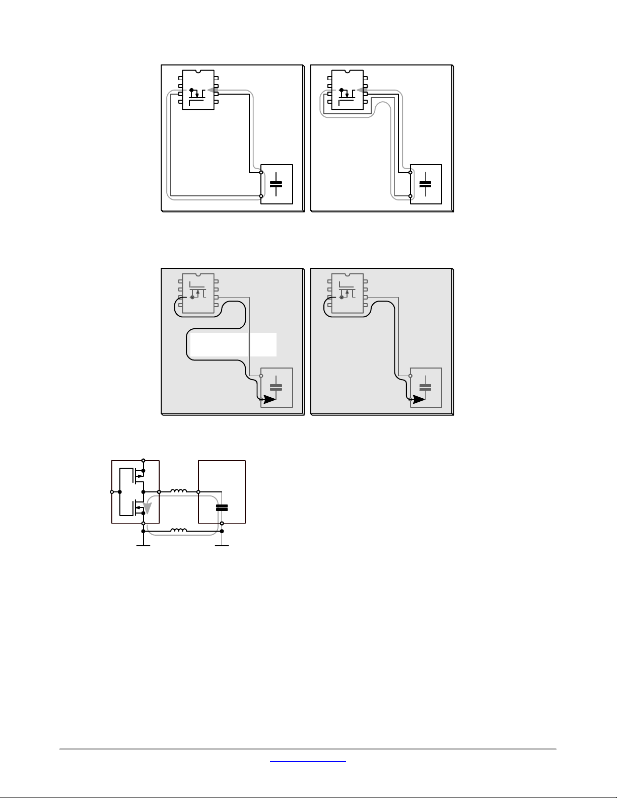
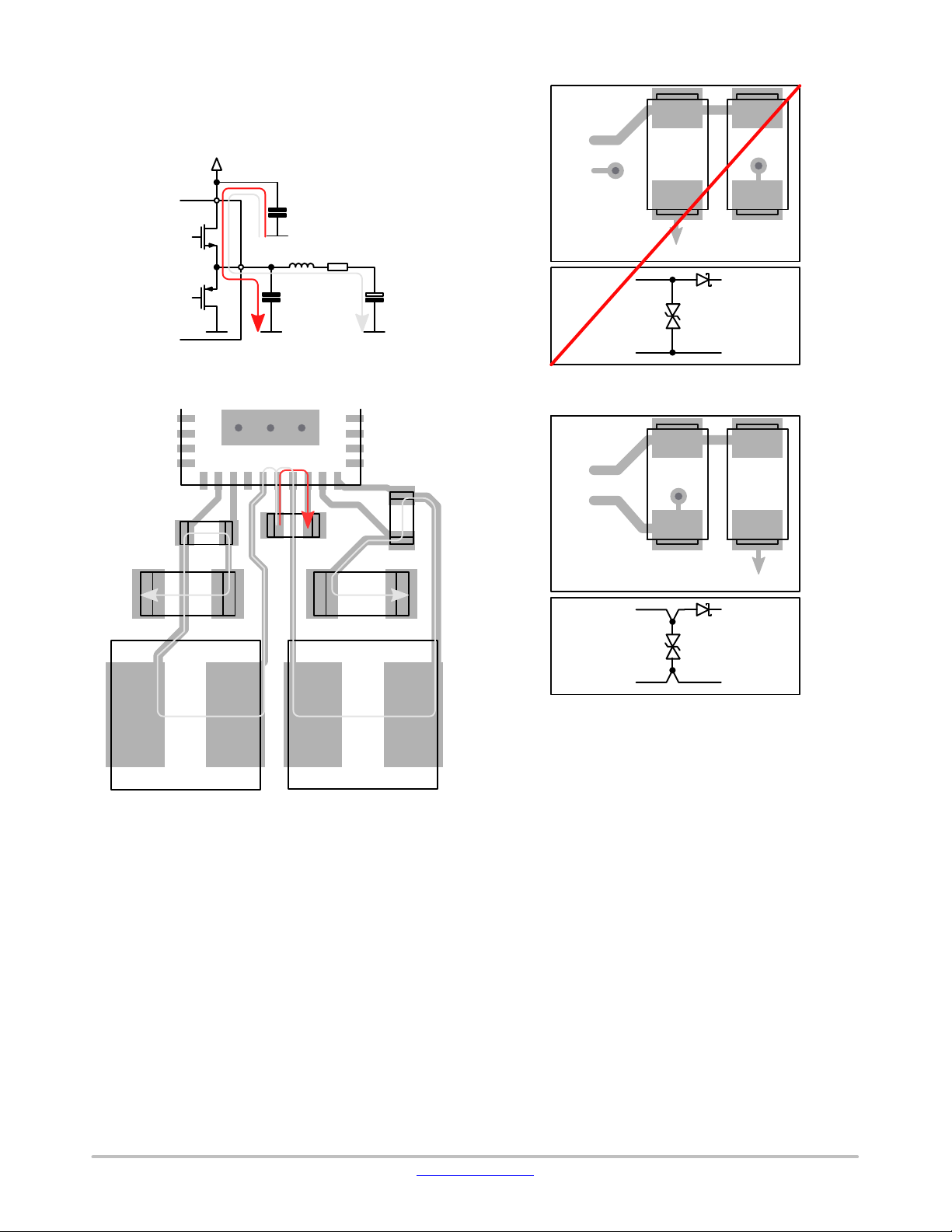
Figure 16 shows an example schematic of an inverter
driving a capacitive load. The PCB tracks going to and
coming from the load will act as an inductor at high
switching frequencies. The return path can be the common
circuit ground, but this is not always the case!
When constructing the PCB layout it is very important to
pay attention to the signal return path.
The first situation in Figure 14 shows a single-layer
design. Here the signal and return path form a large loop,
which will act as an antenna at higher frequencies.
2 x 10 kW
Figure 12. An AND Port Can be Used to Combine the
Signals Coming from Two GPIO Pins
www.onsemi.com
7
Page 8
EVBUM2715/D
Single−layer design
Signal
Return
Single−layer optimized
Signal
Return
Figure 14. Optimizing the Return Path in a Single-layer Design
Dual−layer design
Signal
Dual−layer optimized
Signal
Return
Return
Figure 15. Optimizing the Return Path in a Dual-layer Design
Inverter Load
Signal
Z
PCB
Return
Z
PCB
Figure 16. Inverter Principle Schematic Showing
a Critical Current Loop
This layout can be improved significantly by routing the
signal and return path close to each other. They should be
routed as if they were a differential pair.
In most circuit designs, the return path for most signals is
the common circuit ground. For these circuits using a twoor four-layer PCB with the main ground on the bottom- or
inner-layer is the recommended choice. It simplifies the
layout work and makes it much easier to create optimal
return paths.
Still care has to be taken during the design, as it is easy to
overlook common mistakes. Figure 15 shows a situation
where there is a slot in the ground plane. The return path now
goes around the slot creating a slot antenna.
Ideally the bottom ground plane should never be
interrupted.
Figure 17 shows the current loops for the two DC-DC
converters on the Arduino shield. All the components on the
shield are placed and routed to minimize the loop surface
areas.
When the DC-DC converter switches on its top transistor,
the instantaneous current spike is drawn from the small
100 nF capacitor C8. As these current spikes are short, they
will have a high frequency. So the most critical loop, is the
current flowing from C8 into the parasitic capacitance at
V
as shown in red. To keep this loop very small, C8 must
SW
be placed as close as possible to the VIN-pin. If possible,
place it right next to it as in Figure 18.
Keeping all the tracks on the top layer avoids any
disruptions in the bottom ground layer and resistance/
inductance being added by vias. The two grey arrows show
the larger current loops created by the DC-DC converter.
These should also be kept as short as possible to minimize
radiated emissions. Figure 18 shows the optimal layout,
used on the shield, to keep these loops small.
www.onsemi.com
8
Page 9
EVBUM2715/D
The larger buffer capacitor C9 can be placed further away
from the VIN-pin, as long as the small ceramic capacitor C8
is placed very close to it.
Vin
C8
KNX+
KNX*
D1
D2
L3
Cpar
R21
C12
Vsw
Figure 17. Schematic Showing the DC-DC Converter
Current Loops
VDD2
C11
R20
VDD2MC
VSS2
VSW2
VIN
VSW1
VSS1
C8
VDD1
VDD1M
R21
C12
To VBUS
D1
D2
Figure 19. Wrong Layout for the TVS Diode
D2
KNX+
KNX*
D1
To VBUS
D1
D2
L2
L3
Figure 18. DC-DC Converter Current Loops on the
Arduino Shield
TVS Diode
It is important to optimize the layout of the Transient
Voltage Suppression (TVS) diode in order to effectively
protect the transceiver against surges. When a surge occurs,
the TVS diode must clamp the voltage to a level which
doesn’t damage the transceiver. To achieve this, the series
resistance should be as low as possible.
This can be done by connecting KNX-directly to the TVS
diode before being routed to the rest of the PCB ground as
shown in Figure 20. This ensures that the current path to the
TVS has the lowest resistance and no transient current will
flow to the transceiver.
Figure 20. Optimal Layout for the TVS Diode
GETTING STARTED
The Arduino shield comes with demo software developed
by Tapko Technologies GmbH. The software includes
a demo version of KAIstack which runs on
a STM32F103-NUCLEO board. This software contains all
the necessary software components to connect to the
KNX-bus and comes with a variety of demo applications.
The demo version of KAIstack can be used to start
developing custom application software.
The following limitations apply to the demo version:
• Limited to 16 group addresses, 16 associations and 16
communication objects instead of 255.
• Application interface objects have been removed.
• The rout-count is set to zero in the network layer, limiting
the application use to only one line.
• There are no repetitions on the transport layer.
• It is not possible to change the individual address of the
device through ETS.
• Only one derivative is supported.
www.onsemi.com
9
Page 10
EVBUM2715/D
Prerequisites
Listed below are all the components needed to construct
a small KNX-network with the NCN5100ASGEVB.
• KNX power supply (including a choke).
• USB-KNX interface to communicate with ETS on the
PC.
• A demo version of ETS.
• STM32F103-NUCLEO board to plug the shield into.
• Any version of the NCN5100ASGEVB.
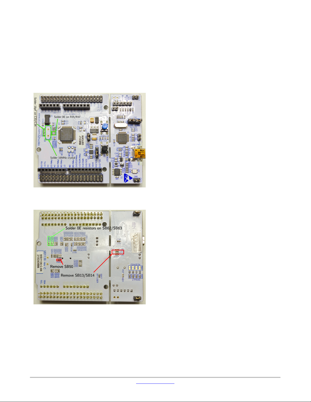
Figure 21. Hardware Modifications on the Top Side of
the Nucleo Board
To meet the timing requirements to communicate on the
KNX-bus, it is mandatory to have a more accurate clock than
the on provided by the internal RC-oscillator of the
microcontroller. Two options are suggested below.
Placing a Crystal
Mount a crystal in the X3 footprint on the Nucleo board.
This crystal must have a frequency of 16 MHz. For the
recommended value of the loading capacitors C33/C34,
refer to the datasheet of the crystal. A good crystal is the
9B-16.000MEEJ-B, which needs loading capacitors of
18 pF.
To get the crystal working on the Nucleo board the
following configuration is required (Figures 21 and 22):
• Place 0 W resistors at R35 and R37.
• Solder the loading capacitors on C33 and C34.
• Remove the 0 W resistor at SB50.
• Solder the crystal on X3.
Apply An External Clock
The second option is to use an external clock.
Use the XCLK-output of the KNX-transceiver as a clock
input for the microcontroller. By tying the XCLKC-pin
high/low a clock frequency of 16 MHz or 8 MHz can be
selected. By default on the Arduino shield, the XCLKC-pin
is pulled high, meaning a clock signal of 16 MHz is present
on the XCLK-pin. This method has the advantage that the
complete application only needs one crystal.
To use the XCLK-output as a clock signal, the following
configuration is required:
• Place a 0 W resistor at SB55.
• Remove the 0 W resistor from SB50.
• Connect the XCLK-pin on the Arduino shield to pin 29 of
CN7 on the Nucleo board. Do this using a wire which is
as short as possible.
UART Communication
On the Nucleo board the USART2 interface is by default
used to communicate with the on-board ST-LINK. This
means that it is not possible to use D0 and D1 on the Arduino
headers for UART communication, as they are not
connected.
To enable UART communication on the Arduino headers
execute the following steps (Figures 21 and 22):
• Remove the 0 W resistors from SB13 and SB14.
• Mount 0 W resistors at SB62 and SB63.
Figure 22. Hardware Modifications on the Bottom
Side of the Nucleo Board
Hardware Modifications
To get started with the demo software, a NCN5110,
NCN5121 or NCN5130 Arduino shield is required in
combination with a STM32F103-NUCLEO board. In order
to get the software running on the microcontroller, a couple
of hardware modifications are required.
www.onsemi.com
These steps will disable the communication between the
microcontroller and the ST-LINK. Then it is no longer
possible to use the Virtual COM-port on the Nucleo board.
To keep using the Virtual COM-port, connect another
USART peripheral to the ST-LINK. USART3 is a possible
candidate which can be used by connecting two wires as
follows:
• Connected pin 1 of CN7 (PC10-USART3_TX) to the RX
pin on CN3.
10
Page 11
EVBUM2715/D
• Connected pin 2 of CN7 (PC11-USART3_RX) to the TX
pin on CN3.
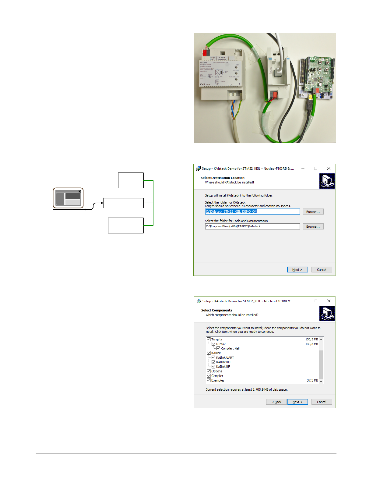
Setting Up A Network
Once the STM32F103-NUCLEO board is ready, a small
network can be set up to get started with the
NCN5100ASGEVB.
Connecting Power
There are several options to power the Nucleo board.
Refer to Section Power for all the possible configurations.
To get started, remove the jumpers J10 and J11 from the
Arduino shield and place JP5 on the Nucleo in the U5V
position. This way the microcontroller will be powered from
the USB port while the KNX-transceiver is powered from
the KNX-bus.
To power the complete solution from the KNX-bus, place
J10 on the Arduino shield and JP5 in the E5V position on the
Nucleo.
Figure 24. Picture of the Practical Setup
ETS
KNX−PSU
USB−KNX interface
NCN5100GEVB
Figure 23. Minimal Network Setup
KNX bus
UART Communication
The demo software from Tapko communicates with the
transceiver at 19.2 kb/s using an even parity bit. Place J1 and
J2 in the ‘0’-position to select the correct communication
speed.
Building The Network
A minimal network setup consists of a KNX power
supply, KNX USB-interface and the NCN5100ASGEVB.
This setup is displayed in Figure 23. The KNX
USB-interface is used to configure the NCN5100ASGEVB
through ETS and to send and receive messages.
After setting up the network, connect the USB coming
from the KNX USB-interface and the Nucleo to the PC. The
physical hardware setup is now complete.
Installing The Software
The microcontroller demo software can be found on the
ON Semiconductor website [5]. Download the software,
unpack it and execute the installer.
The installer will first ask in which folders to install the
software. The first folder will contain KAIstack, the
compiler, software examples and the documentation. In the
second installation folder, some additional tools and the
documentation for KAIstack are installed.
Figure 25. Selection of the Installation Folders
Figure 26. Select which Components to Install
www.onsemi.com
11
Page 12

EVBUM2715/D
Figure 27. Folder Structure of the KAIstack
Installation
Next, the installer gives the option to select which
components to install. It is recommended to leave
everything selected. When clicking on Next, a summary is
given of what will be installed.
Install the software and open the installation folder where
KAIstack is installed. The folder structure will look like the
one shown in Figure 27.
In the appl_example folder, many examples of application
programs can be found. Refer to the documentation included
with the installation on how to modify the software
examples to your needs.
Building and Loading The Software
The folder structure of the first application example
1in1out 07B0 is shown in Figure 28.
Two folders named dummy and tmp contain some
temporary files necessary to compile the program. These
files can be ignored.
The ETS_DB folder contains an ETS-project, that will be
used later on to configure the NCN5100ASGEVB. The
folder named 1_IN_OUT_07B0 contains all the files
necessary to get started in the KNX manufacturer tool. They
can be used to create a catalog entry, product database, etc...
KEIL m Vision IDE. The necessary files are located in the
workspace folder. For more information refer to the
documentation included with the installation.
Lastly there are two batch files included in the folder.
These can be used to build and rebuild the application.
To get started with the previously built setup, one of the
example projects must be loaded in the microcontroller.
Compile the 1in1out_07B0 example by executing the
rebuild.cmd batch file. A command window will pop-up
showing the progress of the compilation process. It will
display a message, as shown in Figure 29 once the
compilation is finished. Now the output folder contains
a .hex file, which can be loaded in the microcontroller.
To program the microcontroller, the
STM32CubeProgrammer tool is used. Open the program
after downloading and installing the latest version. In the
tool click on Open File and select the generated .hex file.
Once it is loaded in the tool, click on the Download button
to load it in the microcontroller. A window saying File
download complete should pop up, as shown in Figure 30.
Now the KNX-device is ready and the network can be
configured.
Figure 29. Output Window of the Compilation
Process
Figure 28. Folder Structure of an Application
Example
The final output files generated by the compiler are placed
in the output folder. The binary that must be loaded in the
microcontroller can be found there.
The application program specific source and header files
are located in the src folder. A file named project.h contains
all the project specific settings.
These projects are all compiled using the ARM KEIL
compiler. It is possible to open the example projects in the
www.onsemi.com
Figure 30. Program the Nucleo Using the
STM32CubeProgrammer
12
Page 13

EVBUM2715/D
Figure 31. Import the ETS-project Included with the Demo Application
Figure 32. The 1-in 1-out ETS-project
ETS Configuration
Configuring a KNX-network is done through ETS. ETS
is a PC tool used by certified KNX-installers to set up
a network. To get started, only the basics are explained here.
For more information, refer to the official
KNX-documentation [4].
The ETS project that is included with the demo
application has to be imported. Click on the import button
shown in Figure 31. Now select the Test Project
1_IN_1_OUT_07B0.knxproj File in the ETS DB folder.
When the import is finished the project will appear in the
Projects pane. Double click on the project to open it.
Because ETS is an installer tool, it is possible to create
complete building structures. This makes it easy to keep
a good overview of the whole installation and to make
modifications in the future. This building structure is created
in the Buildings pane on the left.
The NCN5100ASGEVB device can be found under
Dynamic Folders → Not assigned to a room. To be able to
use and configure it, it has to be assigned to a room first.
A room can not exist on it’s own and must be created inside
a building. To create a building, click on the word Buildings
and then Add Buildings. Once the building is created, right
click on it and select Add → Rooms to create a room.
To assign NCN5100ASGEVB to the room just created,
click on the Not assigned to a room folder and drag the
device into the room. After the device is linked to a room, an
individual address must be assigned to it.
The individual address has a fixed format, and is chosen
in such a way that it reflects it’s position in the network. It
is only used for programming the device. For more
information on this topic, refer to the official
KNX-documentation [4].
The Tapko demo stack doesn’t support changing the
individual address. So the device must be given the fixed
individual address 1.5.8 as shown in Figure 33. Click on the
device in the Buildings panel so that the Properties panel
opens on the right. Under the settings tab the individual
address can be found.
Figure 33. Assigning an Individual Address to the
NCN5100ASGEVB
www.onsemi.com
13
Page 14

EVBUM2715/D
Now the group addresses have to be assigned in order for
the device to communicate on the bus. Refer to the official
KNX-documentation [4] for more information on how the
communication system with group addresses works. Click
on the device in the Buildings panel and go to it’s Group
Objects tab, as shown in Figure 34. It will show all the
supported group objects and the group addresses which are
assigned to it. The assigned group addresses will be blank.
To assign a group address to a group object, right click on it
and select Link with.... A window as shown in Figure 35 will
pop up. In this window, select New. In this tab a new group
address can be created which will be immediately assigned
to the group object. Assign group address 0/0/2 to the bit
group object and 0/0/1 to the switch group object. Give them
both an appropriate name. The switch group object is used
to send a bit value on the bus every time the button SW3 is
pressed. The bit group object is used to control LED3 on the
shield.
It is possible to review and adjust the group
addresses/names in the Group Addresses panel (Workplace
→ Open New Panel).
Figure 35. Assign a New Group Address
Now the complete project has been configured and should
look like Figure 34. This configuration can now be loaded
in the NCN5100ASGEVB. Make sure that the USB-KNX
interface is connected to the PC. Right click on the device in
ETS and select Download → Full download.
Figure 34. The ETS-project after Completing
the Set Up
Figure 37. The Group Monitor Showing the Group Communication on the Bus
Figure 36. Downloading the Full Configuration in the
NCN5100ASGEVB
www.onsemi.com
14
Page 15

EVBUM2715/D
ETS will now ask to press the programming button on the
NCN5100ASGEVB. It can be found on the lower left corner
of the shield. After pressing the button, the LED above will
light up. Now ETS will start the download process.
Once the download has finished, open the Diagnostics
panel by clicking on the Diagnostics button on the top menu
bar. In this panel it is possible to monitor what happens on
the network and control the network through the USB-KNX
interface. Press the Start button to start monitoring the
network.
Now every time button SW3 on the shield gets pressed
a message is sent on the bus by the NCN5100ASGEVB. The
Diagnostics panel shows who is sending the message, what
group address is being sent and what value. The value should
toggle between On and Off every time the button is pressed.
It is possible to send messages on the bus through the
Diagnostics panel to control one of the LEDs on the shield.
In the Group Address field enter 0/0/2.
When pressing the Read button, the USB-KNX interface
sends a read request on the bus for group object 0/0/2. The
NCN5100ASGEVB will respond with the current state of
LED3, which is Off.
In the Value field enter 1. When the Write button is
pressed, the USB-KNX interface sends group object 0/0/2
on the bus with the value On. LED3 on the shield should now
light up. When pressing the Read button again the device
will now respond with On.
BIBLIOGRAPHY
Standards
[1] The KNX Standard v2.1 − KNX Hardware
Requirements and Tests − Part 4−1: Safety
and Environmental Requirements − General.
KNX, 2013.
[2] The KNX Standard v2.1 − System Conformance Testing − Part
8−2−2: Medium Dependant Layers Tests − TP1 Physical and
Link Layer Tests.
KNX, 2013.
Internet
[3] KNX Association. 2020, accessed January 28, 2020. url:
https://www.knx.org
[4] KNX Training Centres. 2020, accessed January 28, 2020. url:
https://www.knx.org/knx−en/
for−professionals/community/training−centres/
index.php.
[5] Wired connectivity solutions. 2020, accessed
January 28, 2020. url: https://www.onsemi.com/
PowerSolutions/segment.do?method=subSolution&
segmentId=IoT&solutionId=19116&subSolutionId=
19126.
.
APPENDIX A − MICROCONTROLLER NET LIST NCN5100AS-1
Table 4. MICROCONTROLLER PINS LIST
Pin Arduino Headers Connected to Function MCU Pin Direction
D0/RX SDO/TXD UART receive line IN
D1/TX SDI/RXD UART transmit line OUT
D2 SAVEB Save data indication IN
D3/PWM LED5 CH2 Red up button LED OUT
D4 SW4 Up button CH2 IN
D5/PWM LED3 CH2 Yellow down button LED OUT
D6/PWM LED2 CH1 Green down button LED OUT
D7 SW1 Down button CH1 IN
D8 SW3 Up button CH1 IN
D9/PWM LED4 CH1 Orange up button LED OUT
D10/CS CSB/UC1 SPI chip select IN
D11/MOSI SDO/TXD SPI MOSI IN
D12/MISO SDI/RXD SPI MISO OUT
D13/SCK SCK/UC2 SPI clock IN
A0 ANAOUT Analog multiplexer output IN (analog)
A1 SW2 Down button CH2 IN
A2 TREQ Transmission request OUT
A3 LED6 Programming LED OUT
A4 S1 Programming button IN
www.onsemi.com
15
Page 16

EVBUM2715/D
APPENDIX B − MICROCONTROLLER NET LIST NCN5100AS-2
Table 5. MICROCONTROLLER PINS LIST
Pin Arduino Headers Connected to Function MCU Pin Direction
D3/PWM LED5 CH2 Red up button LED OUT
D4 SW4 Up button CH2 IN
D5/PWM LED3 CH2 Yellow down button LED OUT
D6/PWM LED2 CH1 Green down button LED OUT
D7 SW1 Down button CH1 IN
D8 SW3 Up button CH1 IN
D9/PWM LED4 CH1 Orange up button LED OUT
D11 RXD2 Data input NCN5110 OUT
D12 RXD1 Data input NCN5110 OUT
A0 TXD Data output NCN5110 IN
A1 SW2 Down button CH2 IN
A3 LED6 Programming LED OUT
A4 S1 Programming button IN
www.onsemi.com
16
Page 17

Table 6. TESTED PLATFORMS
Manufacturer Development Board Microcontroller
STMicroelectronics NUCLEO−F103RB STM32F103RB
Cypress CY8CKIT−044 CY8C4247AZI−M485
Waveshare XNUCLEO−F103RB STM32F103RB
EVBUM2715/D
APPENDIX C − LIST OF TESTED PLATFORMS
www.onsemi.com
17
Page 18

UART-version
8
7
6
5
Place this as close
4
3
2
1
C2
10pF
as possible to the chip!
16MHz
X1
FA−238
1 3
2 4
10pF
C1
XTAL1 XTAL2
XTAL oscillator
GND GND
R1
3V3
A A
9−bit, 19200bps
9−bit, 38400bps
8−bit, 19200bps
8−bit, 38400bps
110
0
010
1
UC1 UC2
Use these to select the baud rate and
parit bit in UART mode.
123
J2
UC2
3V3
3V3
GND
10k
R5
SCK/UC2CS/UC1
123
UC1
J1
Arduino headersArduino headers
GND
10k
R4
Baud rate/parity bit select
C4
3V3
GND
0ER8
1
J3
TP3
XCLK
XCLK
XSEL
XTAL2
XTAL1
D2
RESETB
FANIN
TP1
FANIN
R3
GND
10k
R2
560E
1
ANAOUT
10k
3V3
TP2
C3
3V3
0ER7
0ER6
GND
2
3
Q1
NDS355AN
EVBUM2715/D
APPENDIX D − NCN5130ASGEVB
Red
LED1
750E
R14
3V3
Power LED
123456789
SCL/D15
SDA/D14
Populate for
100nF
U1
31
32
33
34
35
36
37
38
39
40
100nF
Place diode and TVS as close
as possible to the common mode choke!
9V
3V3S
IOREF
1234567
J4
10
AVDD
GND
SCK/D13
MISO/D12
PWM/MOSI/D11
PWM/CS/D10
PWM/D9D8D7
560ER9
560ER11
560ER12
560ER13
SPI
TP4
SCK/UC2
CS/UC1
TP7
GND
CS/UC1
SCK/UC2
MOSI/TXD
TREQ
MODE2
MISO/RXD
25
30
26
29
27
24
28
TREQ
VDDD
VSSD
SDI/RXD
CSB/UC1
SCK/UC2
SDO/TXD
XCLK
XSEL
XTAL2
XTAL1
SAVEB
RESETB
FANIN
ANAOUT
VDDA
VSSA1VBUS22TXO3CCP4CAV5VBUS16CEQ17CEQ28VFILT9V20V
VBUS
TXO
CAV
CCP
CEQ1
GND
C6
27ER10
47nF, 50VC5220nF, 50V
TP5
VBUS
D1
SS16T3G
CAV TP8
TP6
L1
1 2
4 3
KNX−
KNX+
J5
KNX−Bus
MBR0530T
D3
NRST
5VS
VIN
8
Power
MODE1
CEQ2
VFILT
J6
TP9
TRIG
22
MODE123MODE2
VFILT
GND
B B
GND
VLMS30J1L2−GS08
Mode select
1234567
MISO/RXD
TP10
XCLKC
21
TRIG
XCLKC
10
V20V
SMAJ40CA
D2
J7
PWM/D6
PWM/D5D4PWM/D3D2TX/D1
MOSI/TXD
TP11
TRIG
VDD1M
VDD1
VSS1
VSW1
VIN
VSW2
VSS2
VDD2
VDD2MC
VDD2MV
1μF, 50V
C10
100μF, 35V
C9
100nF
C8
100nF
C7
560ER15 TREQ
A0A1A2A3A4
12345
Populate for
UART
NCN5130
20
19
18
17
16
15
14
13
12
11
50V
50V
TP12
TREQ
Populate
for SPI
A5
6
560ER16
TP14
TP13
GND
8
RX/D0
560ER17
3V3
VDD1MV
GND GND
VDD2MV
J8
TP17
GND
TP16
GND
GND
TP15
TP19
GND
Analog in
J9
VDD2
123
3V3
3V3
3V3
C12
10μF
GND
GND
TP18
1E
R21
L3
L2
1E
R20
130k
R18
10μF
C11
GND
GND
691214110003
GND
GND
GND
GND
R19
GND GND
User buttons and LEDs
Figure 38. Schematic
2 x 220 uH, 0.4 A
R22
3V3S
3V3S
3V3S
3V3S
CH1 CH2
R25
R24
R23
GND
20k
Populate for SPI
0E
MODE2MODE1
0E
0E
XCLKC
3V3S
Supply select
9V
GND
10k
R29
PWM/D3PWM/D5PWM/D6 PWM/D9
10k
R27
10k
R28
10k
R26
−
11
Revision
Sheet ofA3
8
Size
Populate for UART
0E
R32
0E
R31
0E
R30
1
2
J11
1
2
J10
SW4
D4D7 D8
Red
LED5
750E
R36
SW2
A1
Yellow
LED3
560E
R34
SW3
Orange
LED4
750E
R35
SW1
Green
LED2
680E
R33
C C
UART
SPI 500kpbs
GND
0
0
10
Select the desired communication mode
GND
TREQ MODE1MODE2
TREQ
0
GND
In this configuration DC−DC2 will generate 9V
and supply the microcontroller board through
the VIN pin on the Arduino headers.
In this configuration the 3,3V generated by DC−DC1
is connected to the 3V3 pin on the Arduino headers.
Make sure your micrcontroller board can be directly
J10 J11
VLMS30J1L2−GS08
VLMA3100−GS08
VLMO30L1M2−GS08
VLMC3100−GS08
J10 J11
GND
GND
GND
GND GNDGND GND
3V3S
R37
A3
GND
Prog
ON Semiconductor — Energy Management Products
1
8MHz
16MHz
Default
1
XLCKC01
XCLK frequency selection
supplied through the 3V3 pin. Else you could damage it!
S1
10k
A4
1
2
Red
LED6
680E
R38
KPT−1608EC
D D
Tijl Schepens
A: NCN5130−UART
KNX Arduino shield
Design
Board ncn5100as−1
Variant
GND GND
Programming button/LED
7
17/10/2019
Date
6
5
4
3
2
1
www.onsemi.com
18
Page 19

Table 7. BILL OF MATERIALS UART-VERSION
Designator
J1 1 WR−PHD 2.54 mm THT Pin Header, 3p 61300311121
J2 1 WR−PHD 2.54 mm THT Pin Header, 3p 61300311121
J3 1 WR−PHD 2.54 mm THT Pin Header, 1p 61300111121
J4 1 Board-To-Board Connector, 2.54 mm,
Qty Description Value Part Number
8 Contacts, Receptacle, Through Hole, 1 Rows
EVBUM2715/D
SSQ−110 −03−G−S
J6 1 Board-To-Board Connector, 2.54 mm,
J7 1 Board-To-Board Connector, 2.54 mm,
J8 1 Serie 2141 − 3.50 mm Horizontal Entry Modular
J9 1 Board-To-Board Connector, 2.54 mm,
L2 1 SMT Power Inductor WE−LQFS, size 4828,
L3 1 SMT Power Inductor WE−LQFS, size 4828,
Q1 1 N-Channel Logic Level Enhancement Mode
J10, J11 2 WR−PHD 2.54 mm THT Pin Header, 2p
R6, R7, R8, R23,
R31, R32
C10 1 Capacitor
D1 1 Schottky Rectifier, Singel 60 V, 1 A,
R20, R21 2 Resistor
LED3 1 LED, Yellow, SMD, 2 mA, 2.2 V, 594 nm 2 mA, 2.2 V, 594 nm VLMA3100−GS08
R19 1 2 (1 x 2) Position Shunt Connector
LED4 1 LED, Orange, SMD, 2.4 mm, 2 mA, 1.8 V,
LED2 1 LED, Green, SMD, 2.4 mm, 2 mA, 1.9 V, 575
C11, C12 2 Capacitor
R2, R3, R4, R5,
R26, R27, R28,
R29, R37
10 Contacts, Receptacle, Through Hole,
1 Rows
6 Contacts, Receptacle, Through Hole, 1 Rows
with Rising Cage Clamp WR−TBL, 3 pin
8 Contacts, Receptacle, Through Hole, 1 Rows
220 mH, 0.4 A
220 mH, 0.4 A
Field Effect Transistor, 30 V, 1.7 A, −55°C to
150°C, 3-Pin SOT−3, RoHS, Tape and Reel
6 Resistor
DO−214AC, 2 Pins, 720 mV
Non-Insulated 0.400 in (10.16 mm) Gold
609 nm
nm
9 Resistor
0 W
1 mF, 50 V
1 A / 720 mV / 60 V SS16T3G
1 W
2 pins D3082−05
2.4 mm, 2 mA, 1.8 V,
609 nm
2.4 mm, 2 mA, 1.9 V,
575 nm
10 mF
10 W
SSQ−110 −03−G−S
SSQ−106−03−G−S
691214110003
SSQ−108−03−G−S
74406043221
74406043221
NDS355AN
RC0603JR−070RL
GCM21BR71H105KA03L
RC0603FR−071RL
VLMO30L1M2−GS08
VLMC3100−GS08
C3216X7R1E106K160AE
CRCW060310K0FKEA
C1, C2 2 Capacitor 10 pF C0402C100J5GACTU
SW1, SW2, SW3,
SW4
X1 1 Crystal Oscillator, 16 MHz, Low Profile SMD,
R22 1 Resistor
R10 1 Resistor
U1 1 Transceiver for KNX Twisted Pair Networks 40 pins NCN5130MNTWG
4 Switch 12 V, 50 mA MCDTS6−3N
3.2 mm 2.5 mm, 30 ppm, 12.5 pF, 50 ppm,
FA−238 Series
16 MHz to 60 MHz /
Load: 12.5 pF /
Stability: 30 ppm /
Tolerance: 50 ppm
20 W
27 W
Q22FA23800181 FA−238
CRCW060320K0FKEA
352027RJT
www.onsemi.com
19
Page 20

EVBUM2715/D
Table 7. BILL OF MATERIALS UART-VERSION (continued)
Designator Part NumberValueDescriptionQty
D2 1 SMAJ40CA − TVS Diode, TRANSZORB SMAJ
Series, Bidirectional, 40 V, 64.5 V, DO−214AC,
2 Pins
C5 1 Capacitor 47 nF, 50 V CGA3E2X7R1H473K080AA
C9 1 Capacitor
S1 1 6.0 x 3.8 mm SMD J−Bend WS−TASV
C3, C4 2 Capacitor 100 nF CC0402KRX7R7BB104
C8 1 Capacitor 100 nF, 50 V VJ0603Y104KXACW1BC
C7 1 Capacitor 100 nF, 50 V VJ0603Y104KXACW1BC
R18 1 Resistor
C6 1 Capacitor 220 nF, 50 V CGA3E3X7R1H224K080AB
R1, R16, R17, R34 4 Resistor
LED6 1 Surface Mount Chip LED, Red 0603, Red KPT−1608EC
R33, R38 2 Resistor
R14, R35, R36 3 Resistor
J5 1 Male connector for WAGO 243−211 Pitch: 5.75 mm /
LED1, LED5 2 LED, Red, 2.4 mm, 636 nm, 1.8 V, 2 mA,
18 mcd
D3 1 Surface Mount Schottky Power Rectifier Uf = 430 mV,
40 V, 400 W SMAJ40CA
100 mF, 35 V
100 mW, 250 V (AC)
130 W
560 W
680 W
750 W
Diameter:1 mm / 100 V /
6 A
Red, 1.8 V, 2 mA VLMS30J1L2−GS08
If = 500 mA, Ur = 30 V
EEEFT1V101AP
434 123 025 816
CRCW0603130KFKEA
CRCW0603560RFKEA
CRCW0603680RFKEA
CRCW0603750RFKEA
13.14.125
MBR0530T1G
www.onsemi.com
20
Page 21

SPI-version
8
7
6
5
4
3
2
1
10pF
C2
Place this as close
as possible to the chip!
16MHz
FA−238
1 3
2 4
10pF
C1
XTAL1 XTAL2
XTAL oscillator
3V3
9−bit, 19200bps
9−bit, 38400bps
8−bit, 19200bps
8−bit, 38400bps
110
0
010
1
UC1 UC2
Use these to select the baud rate and
parit bit in UART mode.
123
UC2
J2
3V3
10k
R5
SCK/UC2CS/UC1
123
UC1
J1
3V3
10k
R4
Baud rate/parity bit select
GND
0ER8
1
J3
X1
FANIN
TP1
GND GND
10k
R3
GND
0ER7
0ER6
GND
10k
R2
2
560E
R1
1
3
Q1
A A
GND
GND
3V3
TP3
XCLK
TP2
3V3
3V3
NDS355AN
3V3
Power LED
123456789
SCL/D15
SDA/D14
AVDD
GND
SCK/D13
MISO/D12
PWM/MOSI/D11
Arduino headersArduino headers
100nF
C4
U1
31
32
XCLK
33
XSEL
XTAL2
34
XTAL1
35
D2
36
37
RESETB
FANIN
38
ANAOUT
39
40
100nF
C3
J4
PWM/CS/D10
560ER9
560ER11
560ER12
560ER13
Populate for
SPI
SCK/UC2
TP4
GND
CS/UC1
SCK/UC2
MOSI/TXD
MISO/RXD
30
26
29
28
27
VDDD
VSSD
SDI/RXD
CSB/UC1
SCK/UC2
SDO/TXD
XCLK
XSEL
XTAL2
XTAL1
SAVEB
RESETB
FANIN
ANAOUT
VDDA
VSSA1VBUS22TXO3CCP4CAV5VBUS16CEQ17CEQ28VFILT9V20V
TXO
CAV
CCP
GND
27ER10
47nF, 50VC5220nF, 50V
TP5
VBUS
D1
SS16T3G
Place diode and TVS as close
as possible to the common mode choke!
1 2
KNX−
KNX+
J5
9V
D3
3V3S
IOREF
NRST
5VS
VIN
1234567
8
EVBUM2715/D
Red
LED1
750E
R14
10
J6
PWM/D9D8D7
TP9
TP7
CS/UC1
TREQ
MODE1
MODE2
TRIG
24
22
25
TREQ
MODE123MODE2
VFILT
VBUS
CEQ1
CEQ2
C6
VFILT
TP6
CAV TP8
L1
4 3
KNX−Bus
MBR0530T
GND
Power
B B
MISO/RXD
TP10
XCLKC
21
TRIG
XCLKC
10
V20V
SMAJ40CA
D2
J7
VLMS30J1L2−GS08
1234567
PWM/D6
PWM/D5D4PWM/D3D2TX/D1
Populate for
MOSI/TXD
TRIG
TP11
NCN5130
VDD1M
20
VDD1
19
VSS1
18
VSW1
17
VIN
16
VSW2
15
VSS2
14
VDD2
13
VDD2MC
12
VDD2MV
11
1μF, 50V
C10
100μF, 35V
C9
50V
100nF
C8
50V
100nF
C7
TP12
560ER15 TREQ
Populate
A0A1A2A3A4
12345
GND
560ER16
UART
TP14
TP13
GND
TREQ
for SPI
A5
6
8
RX/D0
560ER17
3V3
VDD1MV
GND GND
VDD2MV
J8
TP17
GND
TP16
GND
GND
TP15
TP19
GND
Analog in
J9
VDD2
123
1E
1E
C12
10μF
130k
R18
10μF
C11
691214110003
GND
GND
GND
GND
R19
Mode select
TP18
GND GND
Populate for SPI
0E
R25
3V3
0E
R24
3V3
0E
R23
3V3
GND
3V3S
GND
GND
R21
L3
L2
Supply select
2 x 220 uH, 0.4 A
R20
9V
20k
R22
GND
GND
R29
3V3S
PWM/D3PWM/D5PWM/D6 PWM/D9
R27
3V3S
R28
3V3S
R26
3V3S
CH1 CH2
User buttons and LEDs
Populate for UART
MODE2MODE1
XCLKC
GND
10k
10k
10k
10k
−
11
Revision
Sheet ofA3
8
Size
7
Tijl Schepens
UART
0E
R32
GND
0E
R31
GND
0E
R30
GND
1
2
J11
1
2
J10
SW4
D4D7 D8
Red
LED5
750E
R36
SW2
A1
Yellow
LED3
560E
R34
SW3
Orange
LED4
750E
R35
SW1
Green
LED2
680E
R33
C C
SPI 500kpbs
0
0
10
Select the desired communication mode
TREQ MODE1MODE2
0
TREQ
1
8MHz
XLCKC01
XCLK frequency selection
In this configuration DC−DC2 will generate 9V
and supply the microcontroller board through
the VIN pin on the Arduino headers.
In this configuration the 3,3V generated by DC−DC1
is connected to the 3V3 pin on the Arduino headers.
Make sure your micrcontroller board can be directly
supplied through the 3V3 pin. Else you could damage it!
J10 J11
VLMS30J1L2−GS08
VLMA3100−GS08
VLMO30L1M2−GS08
VLMC3100−GS08
J10 J11
GND
GND
GND
GND GNDGND GND
10k
R37
A4
GND
3V3S
1
A3
680E
R38
Prog
16MHz
Default
1
Red
LED6
D D
B: NCN5130−SPI
Design
Board ncn5100as−1
Variant
ON Semiconductor — Energy Management Products
KNX Arduino shield
S1
2
GND GND
KPT−1608EC
Programming button/LED
17/10/2019
Date
6
5
4
3
2
1
Figure 39. Schematic
www.onsemi.com
21
Page 22

Table 8. BILL OF MATERIALS SPI-VERSION
Designator
J3 1 WR−PHD 2.54 mm THT Pin Header, 1p 61300111121
J4 1 Board-To-Board Connector, 2.54 mm,
Qty Description Value Part Number
8 Contacts, Receptacle, Through Hole, 1 Rows
EVBUM2715/D
SSQ−110 −03−G−S
J6 1 Board-To-Board Connector, 2.54 mm,
J7 1 Board-To-Board Connector, 2.54 mm,
J8 1 Serie 2141 − 3.50 mm Horizontal Entry Modular
J9 1 Board-To-Board Connector, 2.54 mm,
L2 1 SMT Power Inductor WE−LQFS, size 4828,
L3 1 SMT Power Inductor WE−LQFS, size 4828,
Q1 1 N-Channel Logic Level Enhancement Mode
J10, J11 2 WR−PHD 2.54 mm THT Pin Header, 2p
R6, R7, R8, R23,
R25, R31
C10 1 Capacitor
D1 1 Schottky Rectifier, Singel 60 V, 1 A,
R20, R21 2 Resistor
LED3 1 LED, Yellow, SMD, 2 mA, 2.2 V, 594 nm 2 mA, 2.2 V, 594 nm VLMA3100−GS08
R19 1 2 (1 x 2) Position Shunt Connector
LED4 1 LED, Orange, SMD, 2.4 mm, 2 mA, 1.8 V,
LED2 1 LED, Green, SMD, 2.4 mm, 2 mA, 1.9 V,
C11, C12 2 Capacitor
R2, R3, R26, R27,
R28, R29, R37
C1, C2 2 Capacitor 10 pF C0402C100J5GACTU
SW1, SW2, SW3,
SW4
X1 1 Crystal Oscillator, 16 MHz, Low Profile SMD,
R22 1 Resistor
R10 1 Resistor
U1 1 Transceiver for KNX Twisted Pair Networks 40 pins NCN5130MNTWG
D2 1 SMAJ40CA − TVS Diode, TRANSZORB SMAJ
C5 1 Capacitor 47 nF, 50 V CGA3E2X7R1H473K080AA
10 Contacts, Receptacle, Through Hole, 1
Rows
6 Contacts, Receptacle, Through Hole, 1 Rows
with Rising Cage Clamp WR−TBL, 3 pin
8 Contacts, Receptacle, Through Hole, 1 Rows
220 mH, 0.4 A
220 mH, 0.4 A
Field Effect Transistor, 30 V, 1.7 A, −55°C to
150°C, 3-Pin SOT−3, RoHS, Tape and Reel
6 Resistor
DO−214AC, 2 Pins, 720 mV
Non−Insulated 0.400 in (10.16 mm) Gold
2.4 mm, 2 mA, 1.8 V,
609 nm
2.4 mm, 2 mA, 1.9 V,
575 nm
7 Resistor
4 Switch 12 V, 50 mA MCDTS6−3N
3.2 mm 2.5 mm, 30 ppm, 12.5 pF, 50 ppm,
FA−238 Series
Series, Bidirectional, 40 V, 64.5 V, DO−214AC,
2 Pins
0 W
1 mF, 50 V
1 A / 720 mV / 60 V SS16T3G
1 W
2 pins D3082−05
609 nm
575 nm
10 mF
10 W
16 MHz to 60 MHz /
Load: 12.5 pF /
Stability: 30 ppm /
Tolerance: 50 ppm
20 W
27 W
40 V, 400 W SMAJ40CA
SSQ−110 −03−G−S
SSQ−106−03−G−S
691214110003
SSQ−108−03−G−S
74406043221
74406043221
NDS355AN
RC0603JR−070RL
GCM21BR71H105KA03L
RC0603FR−071RL
VLMO30L1M2−GS08
VLMC3100−GS08
C3216X7R1E106K160AE
CRCW060310K0FKEA
Q22FA23800181 FA−238
CRCW060320K0FKEA
352027RJT
www.onsemi.com
22
Page 23

EVBUM2715/D
Table 8. BILL OF MATERIALS SPI-VERSION (continued)
Designator Part NumberValueDescriptionQty
C9 1 Capacitor
S1 1 6.0 x 3.8 mm SMD J−Bend WS−TASV
C3, C4 2 Capacitor 100 nF CC0402KRX7R7BB104
C8 1 Capacitor 100 nF, 50 V VJ0603Y104KXACW1BC
C7 1 Capacitor 100 nF, 50 V VJ0603Y104KXACW1BC
R18 1 Resistor
C6 1 Capacitor 220 nF, 50 V CGA3E3X7R1H224K080AB
R1, R9, R11, R12,
R13, R15, R34
LED6 1 Surface Mount Chip LED, Red 0603, Red KPT−1608EC
R33, R38 2 Resistor
R14, R35, R36 3 Resistor
J5 1 Male connector for WAGO 243−211 Pitch: 5.75 mm /
LED1, LED5 2 LED, Red, 2.4 mm, 636 nm, 1.8 V, 2 mA,
D3 1 Surface Mount Schottky Power Rectifier Uf = 430 mV,
7 Resistor
18 mcd
100 mF, 35 V
100 mW, 250 V (AC)
130 W
560 W
680 W
750 W
Diameter: 1 mm / 100 V /
6 A
Red, 1.8 V, 2 mA VLMS30J1L2−GS08
If = 500 mA, Ur = 30 V
EEEFT1V101AP
434 123 025 816
CRCW0603130KFKEA
CRCW0603560RFKEA
CRCW0603680RFKEA
CRCW0603750RFKEA
13.14.125
MBR0530T1G
www.onsemi.com
23
Page 24

UART-version
8
7
6
5
Place this as close
4
3
2
1
C2
10pF
as possible to the chip!
16MHzX1FA−238
1 3
2 4
10pF
C1
XTAL1 XTAL2
XTAL oscillator
GND GND
R1
3V3
A A
9−bit, 19200bps
9−bit, 38400bps
8−bit, 19200bps
8−bit, 38400bps
110
0
010
1
UC1 UC2
Use these to select the baud rate and
parit bit in UART mode.
123
J2
UC2
3V3
3V3
GND
10k
R5
SCK/UC2CS/UC1
123
UC1
J1
Arduino headersArduino headers
GND
10k
R4
Baud rate/parity bit select
C4
3V3
GND
0ER8
1
J3
TP3
XCLK
XCLK
XSEL
XTAL2
XTAL1
D2
RESETB
FANIN
FANIN
TP1
R3
GND
10k
R2
560E
1
ANAOUT
0E
3V3
TP2
C3
3V3
0ER7
0ER6
GND
2
3
Q1
NDS355AN
EVBUM2715/D
APPENDIX E − NCN5121ASGEVB
Red
LED1
750E
R14
3V3
Power LED
123456789
SCL/D15
SDA/D14
Populate for
100nF
U1
31
32
33
34
35
36
37
38
39
40
100nF
Place diode and TVS as close
as possible to the common mode choke!
9V
3V3S
IOREF
1234567
J4
10
AVDD
GND
SCK/D13
MISO/D12
PWM/MOSI/D11
PWM/CS/D10
PWM/D9D8D7
560ER9
560ER11
560ER12
560ER13
SPI
SCK/UC2
TP4
TP7
CS/UC1
GND
CS/UC1
SCK/UC2
MOSI/TXD
TREQ
MODE2
MISO/RXD
25
30
26
29
24
27
28
TREQ
VDDD
VSSD
SDI/RXD
CSB/UC1
SCK/UC2
SDO/TXD
XCLK
XSEL
XTAL2
XTAL1
SAVEB
RESETB
FANIN
ANAOUT
VDDA
VSSA1VBUS22TXO3CCP4CAV5VBUS16CEQ17CEQ28VFILT9V20V
CCP
CEQ1
VBUS
TXO
CAV
GND
C6
27ER10
47nF, 50VC5220nF, 50V
TP5
VBUS
D1
SS16T3G
CAV TP8
TP6
L1
1 2
4 3
KNX−
KNX+
J5
KNX−Bus
D3
MBR0530T
NRST
5VS
VIN
8
Power
MODE1
CEQ2
VFILT
J6
TP9
TRIG
22
MODE123MODE2
VFILT
GND
B B
MISO/RXD
TP10
XCLKC
21
TRIG
XCLKC
10
V20V
SMAJ40CA
D2
J7
VLMS30J1L2−GS08
1234567
PWM/D6
PWM/D5D4PWM/D3D2TX/D1
Populate for
MOSI/TXD
TP11
TRIG
NCN5121
VDD1M
20
VDD1
19
VSS1
18
VSW1
17
VIN
16
VSW2
15
VSS2
14
VDD2
13
VDD2MC
12
VDD2MV
11
1μF, 50V
C10
100μF, 35V
C9
50V
100nF
C8
50V
100nF
C7
TP12
560ER15 TREQ
Populate
A0A1A2A3A4
12345
GND
560ER16
UART
TP14
TP13
GND
TREQ
for SPI
A5
6
8
RX/D0
560ER17
3V3
VDD1MV
GND GND
VDD2MV
J8
TP17
GND
TP16
GND
GND
TP15
TP19
GND
Analog in
J9
VDD2
123
1E
1E
10μF
C12
130k
R18
10μF
C11
691214110003
GND
GND
GND
GND
R19
Mode select
TP18
GND GND
3V3
3V3
3V3
GND
GND
R21
L3
L2
R20
GND
GND
User buttons and LEDs
2 x 220 uH, 0.4 A
R22
3V3S
3V3S
3V3S
3V3S
CH1 CH2
R25
R24
R23
GND
20k
Populate for SPI
0E
MODE2MODE1
0E
0E
XCLKC
3V3S
Supply select
9V
GND
10k
R29
PWM/D3PWM/D5PWM/D6 PWM/D9
10k
R27
10k
R28
10k
R26
−
11
Revision
Sheet ofA3
8
Size
Populate for UART
0E
R32
0E
R31
0E
R30
1
2
J11
1
2
J10
SW4
D4D7 D8
Red
LED5
750E
R36
SW2
A1
Yellow
LED3
560E
R34
SW3
Orange
LED4
750E
R35
SW1
Green
LED2
680E
R33
C C
UART
SPI 500kpbs
GND
0
0
10
Select the desired communication mode
GND
TREQ MODE1MODE2
TREQ
0
GND
In this configuration DC−DC2 will generate 9V
and supply the microcontroller board through
the VIN pin on the Arduino headers.
In this configuration the 3,3V generated by DC−DC1
is connected to the 3V3 pin on the Arduino headers.
Make sure your micrcontroller board can be directly
J10 J11
VLMS30J1L2−GS08
VLMA3100−GS08
VLMO30L1M2−GS08
VLMC3100−GS08
J10 J11
GND
GND
GND
GND GNDGND GND
3V3S
R37
A3
GND
Prog
ON Semiconductor — Energy Management Products
1
8MHz
16MHz
Default
1
XLCKC01
XCLK frequency selection
supplied through the 3V3 pin. Else you could damage it!
S1
10k
A4
1
2
Red
LED6
680E
R38
KPT−1608EC
D D
Tijl Schepens
C: NCN5121−UART
KNX Arduino shield
Design
Board ncn5100as−1
Variant
GND GND
Programming button/LED
7
21/11/2019
Date
6
5
4
3
2
1
Figure 40. Schematic
www.onsemi.com
24
Page 25

EVBUM2715/D
Table 9. BILL OF MATERIALS UART-VERSION
Designator
J1 1 WR−PHD 2.54 mm THT Pin Header, 3p 61300311121
J2 1 WR−PHD 2.54 mm THT Pin Header, 3p 61300311121
J3 1 WR−PHD 2.54 mm THT Pin Header, 1p 61300111121
J4 1 Board-To-Board Connector, 2.54 mm,
J6 1 Board-To-Board Connector, 2.54 mm,
J7 1 Board-To-Board Connector, 2.54 mm,
J8 1 Serie 2141 − 3.50 mm Horizontal Entry Modular
J9 1 Board-To-Board Connector, 2.54 mm,
L2 1 SMT Power Inductor WE−LQFS, size 4828,
L3 1 SMT Power Inductor WE−LQFS, size 4828,
Q1 1 N-Channel Logic Level Enhancement Mode
J10, J11 2 WR−PHD 2.54 mm THT Pin Header, 2p
R3, R6, R7, R8,
R23, R31, R32
C10 1 Capacitor
D1 1 Schottky Rectifier, Singel 60 V, 1 A,
R20, R21 2 Resistor
LED3 1 LED, Yellow, SMD, 2 mA, 2.2 V, 594 nm 2 mA, 2.2 V, 594 nm VLMA3100−GS08
R19 1 2 (1 x 2) Position Shunt Connector
LED4 1 LED, Orange, SMD, 2.4 mm, 2 mA, 1.8 V,
LED2 1 LED, Green, SMD, 2.4 mm, 2 mA, 1.9 V,
C11, C12 2 Capacitor
R2, R4, R5, R26,
R27, R28, R29,
R37
C1, C2 2 Capacitor 10 pF C0402C100J5GACTU
SW1, SW2, SW3,
SW4
X1 1 16 MHz to 60 MHz /
R22 1 Resistor
R10 1 Resistor
U1 1 Transceiver for KNX Twisted Pair Networks 40 pins NCN5121MNTWG
Qty Description Value Part Number
8 Contacts, Receptacle, Through Hole, 1 Rows
10 Contacts, Receptacle, Through Hole,
1 Rows
6 Contacts, Receptacle, Through Hole, 1 Rows
with Rising Cage Clamp WR−TBL, 3 pin
8 Contacts, Receptacle, Through Hole, 1 Rows
220 mH, 0.4 A
220 mH, 0.4 A
Field Effect Transistor, 30 V, 1.7 A, −55°C to
150°C, 3-Pin SOT−3, RoHS, Tape and Reel
7 Resistor
DO−214AC, 2 Pins, 720 mV
Non-Insulated 0.400 in (10.16 mm) Gold
2.4 mm, 2 mA, 1.8 V,
609 nm
2.4 mm, 2 mA, 1.9 V,
575 nm
8 Resistor
4 Switch 12 V, 50 mA MCDTS6−3N
0 W
1 mF, 50 V
1 A / 720 mV / 60 V SS16T3G
1 W
2 pins D3082−05
609 nm
575 nm
10 mF
10 W
Load: 12.5 pF /
Stability: 30 ppm /
Tolerance: 50 ppm
20 W
27 W
SSQ−110 −03−G−S
SSQ−110 −03−G−S
SSQ−106−03−G−S
691214110003
SSQ−108−03−G−S
74406043221
74406043221
NDS355AN
CRCW06030000Z0EA,
RC0603JR−070RL
GCM21BR71H105KA03L
RC0603FR−071RL
VLMO30L1M2−GS08
VLMC3100−GS08
C3216X7R1E106K160AE
CRCW060310K0FKEA
Q22FA23800181 FA−238
CRCW060320K0FKEA
352027RJT
www.onsemi.com
25
Page 26

EVBUM2715/D
Table 9. BILL OF MATERIALS UART-VERSION (continued)
Designator Part NumberValueDescriptionQty
D2 1 SMAJ40CA − TVS Diode, TRANSZORB SMAJ
Series, Bidirectional, 40 V, 64.5 V, DO−214AC,
2 Pins
C5 1 Capacitor 47 nF, 50 V CGA3E2X7R1H473K080AA
C9 1 Capacitor
S1 1 6.0 x 3.8 mm SMD J−Bend WS−TASV
C3, C4 2 Capacitor 100 nF CC0402KRX7R7BB104
C8 1 Capacitor 100 nF, 50 V VJ0603Y104KXACW1BC
C7 1 Capacitor 100 nF, 50 V VJ0603Y104KXACW1BC
R18 1 Resistor
C6 1 Capacitor 220 nF, 50 V CGA3E3X7R1H224K080AB
R1, R16, R17, R34 4 Resistor
LED6 1 Surface Mount Chip LED, Red 0603, Red KPT−1608EC
R33, R38 2 Resistor
R14, R35, R36 3 Resistor
J5 1 Male connector for WAGO 243−211 Pitch: 5.75 mm /
LED1, LED5 2 LED, Red, 2.4 mm, 636 nm, 1.8 V, 2 mA,
18 mcd
D3 1 Surface Mount Schottky Power Rectifier Uf = 430 mV,
40 V, 400 W SMAJ40CA
100 mF, 35 V
100 mW, 250 V (AC)
130 W
560 W
680 W
750 W
Diameter: 1 mm / 100 V /
6 A
Red, 1.8 V, 2 mA VLMS30J1L2−GS08
If = 500 mA, Ur = 30 V
EEEFT1V101AP
434 123 025 816
CRCW0603130KFKEA
CRCW0603560RFKEA
CRCW0603680RFKEA
CRCW0603750RFKEA
13.14.125
MBR0530T1G
www.onsemi.com
26
Page 27

SPI-version
8
7
6
5
4
3
2
1
C2
10pF
Place this as close
as possible to the chip!
FA−238
16MHz
1 3
2 4
10pF
C1
XTAL1 XTAL2
XTAL oscillator
3V3
9−bit, 19200bps
9−bit, 38400bps
8−bit, 19200bps
8−bit, 38400bps
110
0
010
1
UC1 UC2
Use these to select the baud rate and
parit bit in UART mode.
123
UC2
J2
3V3
10k
R5
SCK/UC2CS/UC1
123
UC1
J1
3V3
10k
R4
Baud rate/parity bit select
GND
0ER8
1
J3
X1
FANIN
TP1
GND GND
0E
R3
GND
0ER7
0ER6
GND
10k
R2
2
560E
R1
1
3
Q1
A A
GND
GND
3V3
TP3
XCLK
3V3
TP2
3V3
NDS355AN
3V3
Power LED
123456789
SCL/D15
SDA/D14
AVDD
GND
SCK/D13
MISO/D12
PWM/MOSI/D11
Arduino headersArduino headers
C4
100nF
U1
31
32
XCLK
33
XSEL
XTAL2
34
XTAL1
35
D2
36
37
RESETB
FANIN
38
ANAOUT
39
40
100nF
C3
J4
PWM/CS/D10
560ER9
560ER11
560ER12
560ER13
Populate for
SPI
SCK/UC2
TP4
GND
CS/UC1
SCK/UC2
MOSI/TXD
MISO/RXD
26
29
30
28
27
VDDD
VSSD
SDI/RXD
CSB/UC1
SCK/UC2
SDO/TXD
XCLK
XSEL
XTAL2
XTAL1
SAVEB
RESETB
FANIN
ANAOUT
VDDA
VSSA1VBUS22TXO3CCP4CAV5VBUS16CEQ17CEQ28VFILT9V20V
CCP
TXO
CAV
GND
27ER10
47nF, 50VC5220nF, 50V
TP5
VBUS
D1
SS16T3G
Place diode and TVS as close
as possible to the common mode choke!
1 2
KNX−
KNX+
J5
9V
D3
3V3S
IOREF
NRST
5VS
VIN
1234567
8
EVBUM2715/D
Red
LED1
750E
R14
10
J6
PWM/D9D8D7
TP9
TP7
CS/UC1
TREQ
MODE1
MODE2
TRIG
25
24
22
TREQ
MODE123MODE2
CEQ1
CEQ2
VFILT
VBUS
C6
VFILT
CAV TP8
TP6
L1
4 3
KNX−Bus
MBR0530T
GND
Power
B B
MISO/RXD
TP10
XCLKC
21
TRIG
XCLKC
10
V20V
SMAJ40CA
D2
J7
VLMS30J1L2−GS08
1234567
PWM/D6
PWM/D5D4PWM/D3D2TX/D1
Populate for
MOSI/TXD
TP11
TRIG
NCN5121
VDD1M
20
VDD1
19
VSS1
18
VSW1
17
VIN
16
VSW2
15
VSS2
14
VDD2
13
VDD2MC
12
VDD2MV
11
1μF, 50V
C10
100μF, 35V
C9
50V
100nF
C8
50V
100nF
C7
TP12
560ER15 TREQ
Populate
A0A1A2A3A4
12345
GND
560ER16
UART
TP14
TP13
GND
TREQ
for SPI
A5
6
8
RX/D0
560ER17
3V3
VDD1MV
GND GND
VDD2MV
J8
TP17
GND
TP16
GND
GND
TP15
TP19
GND
Analog in
J9
VDD2
123
1E
1E
10μF
C12
130k
R18
10μF
C11
691214110003
GND
GND
GND
GND
R19
Mode select
TP18
GND GND
Populate for SPI
0E
R25
3V3
0E
R24
3V3
0E
R23
3V3
GND
3V3S
GND
GND
R21
L3
L2
Supply select
2 x 220 uH, 0.4 A
R20
9V
20k
R22
GND
GND
R29
3V3S
PWM/D3PWM/D5PWM/D6 PWM/D9
R27
3V3S
R28
3V3S
R26
3V3S
CH1 CH2
User buttons and LEDs
Populate for UART
MODE2MODE1
XCLKC
GND
10k
10k
10k
10k
−
11
Revision
Sheet ofA3
8
Size
7
Tijl Schepens
UART
0E
R32
GND
0E
R31
GND
0E
R30
GND
1
2
J11
1
2
J10
SW4
D4D7 D8
Red
LED5
750E
R36
SW2
A1
Yellow
LED3
560E
R34
SW3
Orange
LED4
750E
R35
SW1
Green
LED2
680E
R33
C C
SPI 500kpbs
0
0
10
Select the desired communication mode
TREQ MODE1MODE2
0
TREQ
1
8MHz
XLCKC01
XCLK frequency selection
In this configuration DC−DC2 will generate 9V
and supply the microcontroller board through
the VIN pin on the Arduino headers.
In this configuration the 3,3V generated by DC−DC1
is connected to the 3V3 pin on the Arduino headers.
Make sure your micrcontroller board can be directly
supplied through the 3V3 pin. Else you could damage it!
J10 J11
VLMS30J1L2−GS08
VLMA3100−GS08
VLMO30L1M2−GS08
VLMC3100−GS08
J10 J11
GND
GND
GND
GND GNDGND GND
10k
R37
A4
GND
3V3S
1
A3
680E
R38
Prog
16MHz
Default
1
Red
LED6
D D
D: NCN5121−SPI
Board ncn5100as−1
Variant
ON Semiconductor — Energy Management Products
KNX Arduino shield
Design
S1
2
GND GND
KPT−1608EC
Programming button/LED
21/11/2019
Date
6
5
4
3
2
1
Figure 41. Schematic
www.onsemi.com
27
Page 28

EVBUM2715/D
Table 10. BILL OF MATERIALS SPI-VERSION
Designator
J3 1 WR−PHD 2.54 mm THT Pin Header, 1p 61300111121
J4 1 Board-To-Board Connector, 2.54 mm,
J6 1 Board-To-Board Connector, 2.54 mm,
J7 1 Board-To-Board Connector, 2.54 mm,
J8 1 Serie 2141 − 3.50 mm Horizontal Entry Modular
J9 1 Board-To-Board Connector, 2.54 mm,
L2 1 SMT Power Inductor WE−LQFS, size 4828,
L3 1 SMT Power Inductor WE−LQFS, size 4828,
Q1 1 N−Channel Logic Level Enhancement
J10, J11 2 WR−PHD 2.54 mm THT Pin Header,
R3, R6, R7, R8,
R23, R25, R31
C10 1 Capacitor
D1 1 Schottky Rectifier, Singel 60 V, 1 A,
R20, R21 2 Resistor
LED3 1 LED, Yellow, SMD, 2 mA, 2.2 V, 594 nm 2 mA, 2.2 V, 594 nm VLMA3100−GS08
R19 1 2 (1 x 2) Position Shunt Connector
LED4 1 LED, Orange, SMD, 2.4 mm, 2 mA, 1.8 V,
LED2 1 LED, Green, SMD, 2.4 mm, 2 mA, 1.9 V,
C11, C12 2 Capacitor
R2, R26, R27,
R28, R29, R37
C1, C2 2 Capacitor 10 pF C0402C100J5GACTU
SW1, SW2, SW3, 4 Switch 12 V, 50 mA MCDTS6−3N
SW4 X1 1 16 MHz to 60 Mhz /
R22 1 Resistor
R10 1 Resistor
U1 1 Transceiver for KNX Twisted Pair Networks 40pins NCN5121MNTWG
D2 1 SMAJ40CA − TVS Diode,
C5 1 Capacitor 47 nF, 50 V CGA3E2X7R1H473K080AA
Qty Description Value Part Number
8 Contacts, Receptacle, Through Hole, 1 Rows
10 Contacts, Receptacle, Through Hole,
1 Rows
6 Contacts, Receptacle, Through Hole, 1 Rows
with Rising Cage Clamp WR−TBL, 3 pin
8 Contacts, Receptacle, Through Hole, 1 Rows
220 mH, 0.4 A
220 mH, 0.4 A
Mode Field Effect Transistor, 30 V, 1.7 A,
−55°C to 150°C, 3-Pin SOT−3, RoHS,
Tape and Reel
7 Resistor
DO−214AC, 2 Pins, 720 mV
Non-Insulated 0.400in (10.16 mm) Gold
609 nm
575 nm
6 Resistor
TRANSZORB SMAJ Series,
Bidirectional, 40 V, 64.5 V,
DO−214AC, 2 Pins
0 W
1 mF, 50 V
1 A / 720 mV / 60 V SS16T3G
1 W
2 pins D3082−05
2.4 mm, 2 mA,
1.8 V, 609 nm
2.4 mm, 2 mA,
1.9 V, 575 nm
10 mF
10 W
Load: 12.5 pF /
Stability: 30 ppm /
Tolerance: 50 ppm
20 W
27 W
40 V, 400 W SMAJ40CA
SSQ−110 −03−G−S
SSQ−110 −03−G−S
SSQ−106−03−G−S
691214110003
SSQ−108−03−G−S
74406043221
74406043221
NDS355AN
CRCW06030000Z0EA,
RC0603JR−070RL
GCM21BR71H105KA03L
RC0603FR−071RL
VLMO30L1M2−GS08
VLMC3100−GS08
C3216X7R1E106K160AE
CRCW060310K0FKEA
Q22FA23800181 FA−238
CRCW060320K0FKEA
352027RJT
www.onsemi.com
28
Page 29

EVBUM2715/D
Table 10. BILL OF MATERIALS SPI-VERSION (continued)
Designator Part NumberValueDescriptionQty
C9 1 Capacitor
S1 1 6.0 x 3.8 mm SMD J−Bend WS−TASV
C3, C4 2 Capacitor 100 nF CC0402KRX7R7BB104
C8 1 Capacitor 100 nF, 50 V VJ0603Y104KXACW1BC
C7 1 Capacitor 100 nF, 50 V VJ0603Y104KXACW1BC
R18 1 Resistor
C6 1 Capacitor 220 nF, 50 V CGA3E3X7R1H224K080AB
R1, R9, R11, R12,
R13, R15, R34
LED6 1 Surface Mount Chip LED, Red 0603, Red KPT−1608EC
R33, R38 2 Resistor
R14, R35, R36 3 Resistor
J5 1 Male connector for WAGO 243−211 Pitch: 5.75 mm /
LED1, LED5 2 LED, Red, 2.4 mm, 636 nm, 1.8 V, 2 mA,
D3 1 Surface Mount Schottky Power Rectifier Uf = 430 mV,
7 Resistor
18 mcd
100 mF, 35 V
100 mW, 250 V (AC)
130 W
560 W
680 W
750 W
Diameter: 1 mm / 100 V /
6 A
Red, 1.8 V, 2 mA VLMS30J1L2−GS08
If = 500 mA, Ur = 30 V
EEEFT1V101AP
434 123 025 816
CRCW0603130KFKEA
CRCW0603560RFKEA
CRCW0603680RFKEA
CRCW0603750RFKEA
13.14.125
MBR0530T1G
www.onsemi.com
29
Page 30

Full Option
8
EVBUM2715/D
APPENDIX F − NCN5110ASGEVB SCHEMATIC (FULL OPTION)
−
Revision
11
Sheet ofA3
8
123456789
SCL/D15
SDA/D14
AVDD
7
U2B
5
3V3
100nF
C1
6
5
TP1
FANIN
10k
R3
GND
4
3
GND
10k
R2
560E
R1
3V3
2
1
1
Arduino headersArduino headers
3
GND
16V
100nF,16V
C4
3V3
U1
GND
31
32
33
34
35
D2
36
37
RESETB
FANIN
38
39
40
3V3
TP2
100nF,16V
C3
3V3
0ER6
Place diode and TVS as close
as possible to the common mode choke!
2
3
NDS355AN
Q1
9V
3V3S
IOREF
NRST
1234567
J4
GND
SCK/D13
MISO/D12
PWM/MOSI/D11
PWM/CS/D10
PWM/D9D8D7
&
U2A
MC74HC1G08
A0
560ER4
TP10
TXD
TP9
GND
V20VEN
RXD 560ER5
DC2EN
TXD
26
27
28
25
29
30
TXD
RXD
VDDD
VSSD
DC2EN
V20VEN
XCLK
TEST5
XTAL2
XTAL1
SAVEB
RESETB
FANIN
TEST6
VDDA
VBUS22TXO3CCP4CAV5VBUS16CEQ17CEQ28VFILT9V20V
VSSA
1
CCP
VBUS
TXO
CAV
GND
27ER10
47nF, 50VC5220nF, 50V
TP5
VBUS
D1
SS16T3G
TP6
1 2
4 3
KNX−
KNX+
J5
D3
5VS
VIN
8
10
RXD
24
TEST4
CEQ1
CEQ2
C6
VFILT
CAV TP8
L1
KNX−Bus
MBR0530T
Power
J6
R8
R7
21
TEST122TEST223TEST3
10
VFILT
V20V
GND
1234567
10k
10k
1
2
3
XCLKC
SMAJ40CA
D2
A0A1A2A3A4
12345
J7
PWM/D6
PWM/D5D4PWM/D3D2TX/D1
GND
J1
GND
VDD1M
20
VDD1
19
VSS1
18
VSW1
17
VIN
16
VSW2
15
VSS2
14
VDD2
13
VDD2MC
12
VDD2MV
11
1μF, 50V
C10
47μF, 35V
C9
50V
100nF
C8
50V
100nF
C7
0ER9
A5
6
RX/D0
3V3
3V3
VDD1MV
TP14
GND GND
TP13
VDD2MV
GND
TP7
TP4
TP3
Analog in
8
J9
R120ER15
R11
3V3
VDD2
123
J8
GND
GND
GND
0E
0E
C12
1E
1E
R18
C11
GND
GND
GND
Power LED
DC2EN
V20VEN
TP18
10μF
130k
10μF
691214110003
R19
GND GND
LED1
750E
R14
3V3
GND
0E
R13
GND
GND
GND
GND
3V3S
R21
0ER16
L3
L2
Supply select
2 x 220 uH, 0.4 A
R20
9V
20k
R22
GND
GND
R29
3V3S
PWM/D3PWM/D5PWM/D6 PWM/D9
R27
3V3S
R28
3V3S
R26
3V3S
CH1 CH2
User buttons and LEDs
Size
Red
GND
VLMS30J1L2−GS08
7
Tijl Schepens
A: DC−DC2+V20V
20/09/2019
Board ncn5100as−2
Variant
Date
KNX Arduino shield
ON Semiconductor — Energy Management Products
Design
6
1
2
J11
1
2
J10
and supply the microcontroller board through
In this configuration DC−DC2 will generate 9V
the VIN pin on the Arduino headers.
In this configuration the 3,3V generated by DC−DC1
is connected to the 3V3 pin on the Arduino headers.
Make sure your micrcontroller board can be directly
GND
J10 J11
10k
10k
10k
10k
SW4
D4D7 D8
750E
R36
08
A1
560E
R34
750E
R35
680E
R33
LED5
LED3
LED4
LED2
Red
SW2
Yellow
SW3
Orange
SW1
Green
GND
VLMS30J1L2−GS
GND
VLMA3100−GS08
GND
GND GNDGND GND
VLMO30L1M2−GS08
GND
VLMC3100−GS08
supplied through the 3V3 pin. Else you could damage it!
J10 J11
S1
10k
R37
A4
1
2
Red
LED6
680E
R38
KPT−1608EC
Prog
3V3S
A3
GND GND
5
4
3
2
1
A A
B B
C C
D D
Figure 42. Schematic
www.onsemi.com
30
Page 31

EVBUM2715/D
Table 11. BILL OF MATERIALS FULL VERSION
Designator
J1 1 WR−PHD 2.54 mm THT Pin Header, 03p 61300311121
J4 1 Board-To-Board Connector, 2.54 mm,
J6 1 Board-To-Board Connector, 2.54 mm,
J7 1 Board-To-Board Connector, 2.54 mm,
J8 1 Serie 2141 − 3.50 mm Horizontal Entry
J9 1 Board-To-Board Connector, 2.54 mm,
L2 1 SMT Power Inductor WE−LQFS, size 4828,
L3 1 SMT Power Inductor WE−LQFS, size 4828,
Q1 1 N-Channel Logic Level Enhancement Mode
U2 1 Single 2-Input AND Gate MC74HC1G08DTT1G
J10, J11 2 WR−PHD 2.54 mm THT Pin Header, 2p
R6, R13, R15 3 Resistor
C10 1 Capacitor
D1 1 Schottky Rectifier, Singel 60 V, 1 A, 1 A / 720 mV / 60 V SS16T3G
R20, R21 2 Resistor
LED3 1 LED, Yellow, SMD, 2 mA, 2.2 V, 594 nm 2 mA, 2.2 V, 594 nm VLMA3100−GS08
R19 1 2 (1 x 2) Position Shunt Connector 2 pins D3082−05
LED4 1 LED, Orange, SMD, 2.4 mm, 2 mA, 1.8 V,
LED2 1 LED, Green, SMD, 2.4 mm, 2 mA, 1.9 V,
C11, C12 2 Capacitor
R2, R3, R7, R8,
R26, R27, R28,
R29, R37
SW1, SW2, SW3,
SW4
R22 1 Resistor
R10 1 Resistor
U1 1 Transceiver for KNX Twisted Pair Networks 40 pins NCN5110
D2 1 SMAJ40CA − TVS Diode, TRANSZORB
C9 1 Capacitor
C5 1 Capacitor 47 nF, 50 V
S1 1 6.0 x 3.8 mm SMD J−Bend WS−TASV
C3, C4 2 Capacitor 100 nF, 16 V
Qty Description Value Part Number
8 Contacts, Receptacle, Through Hole, 1 Rows
10 Contacts, Receptacle, Through Hole,
1 Rows
6 Contacts, Receptacle, Through Hole, 1 Rows
Modular with Rising Cage Clamp WR−TBL,
3 pin
8 Contacts, Receptacle, Through Hole, 1 Rows
220 mH, 0.4 A
220 mH, 0.4 A
Field Effect Transistor, 30 V, 1.7 A,
−55°C to 150°C, 3-Pin SOT−3, RoHS,
Tape and Reel
0 W
1 mF, 50 V
1 W
609 nm
575 nm
9 Resistor
4 Switch 12 V, 50 mA MCDTS6−3N
SMAJ Series, Bidirectional, 40 V, 64.5 V,
DO−214AC, 2 Pins
2.4 mm, 2 mA, 1.8 V,
609 nm
2.4 mm, 2 mA, 1.9 V,
575 nm
10 mF
10 W
20 W
27 W
40 V, 400 W SMAJ40CA
47 mF, 35 V
100 mW, 250 V (AC)
SSQ−110 −03−G−S
SSQ−110 −03−G−S
SSQ−106−03−G−S
SSQ−108−03−G−S
VLMO30L1M2−GS08
VLMC3100−GS08
434 123 025 816
www.onsemi.com
31
Page 32

EVBUM2715/D
Table 11. BILL OF MATERIALS FULL VERSION (continued)
Designator Part NumberValueDescriptionQty
C8 1 Capacitor 100 nF, 50 V
C1 1 Capacitor 100 nF, 16 V
C7 1 Capacitor 100 nF, 50 V
R18 1 Resistor
C6 1 Capacitor 220 nF, 50 V
R1, R4, R5, R34 4 Resistor
LED6 1 Surface Mount Chip LED, Red 0603, Red KPT−1608EC
R33, R38 2 Resistor
R14, R35, R36 3 Resistor
LED1, LED5 2 LED, Red, 2.4 mm, 636 nm, 1.8 V, 2 mA,
18 mcd
J5 1 Male connector for WAGO 243−211 Pitch: 5.75 mm /
Diameter: 1 mm / 100 V /
D3 1 Surface Mount Schottky Power Rectifier Uf = 430 mV,
130 W
560 W
680 W
750 W
Led, Red, 1.8 V, 2 mA VLMS30J1L2−GS08
6 A
If = 500 mA, Ur = 30 V
243−211Male
MBR0530T1G
www.onsemi.com
32
Page 33

Minimal BoM Version
8
EVBUM2715/D
−
Revision
11
Sheet ofA3
8
123456789
SCL/D15
SDA/D14
AVDD
7
U2B
5
3V3
100nF
C1
6
5
TP1
FANIN
10k
R3
GND
4
3
GND
10k
R2
560E
R1
3V3
2
1
1
Arduino headersArduino headers
3
GND
16V
C4
100nF,16V
3V3
U1
GND
31
32
33
34
35
D2
36
37
RESETB
FANIN
38
39
40
3V3
TP2
100nF,16V
C3
3V3
0ER6
Place diode and TVS as close
as possible to the common mode choke!
2
3
NDS355AN
Q1
9V
3V3S
IOREF
NRST
1234567
J4
GND
SCK/D13
MISO/D12
PWM/MOSI/D11
PWM/CS/D10
PWM/D9D8D7
&
U2A
MC74HC1G08
A0
560ER4
TP10
TXD
TP9
GND
V20VEN
RXD 560ER5
DC2EN
TXD
26
27
28
25
29
30
TXD
RXD
VDDD
VSSD
DC2EN
V20VEN
XCLK
TEST5
XTAL2
XTAL1
SAVEB
RESETB
FANIN
TEST6
VDDA
VBUS22TXO3CCP4CAV5VBUS16CEQ17CEQ28VFILT9V20V
VSSA
1
CCP
TXO
CAV
VBUS
GND
27ER10
47nF, 50VC5220nF, 50V
TP5
VBUS
D1
SS16T3G
TP6
1 2
4 3
KNX−
KNX+
J5
D3
5VS
VIN
8
10
RXD
24
TEST4
CEQ1
CEQ2
C6
VFILT
CAV TP8
L1
KNX−Bus
MBR0530T
Power
J6
R8
R7
21
TEST122TEST223TEST3
10
VFILT
V20V
GND
1234567
10k
10k
1
2
3
XCLKC
SMAJ40CA
D2
A0A1A2A3A4
12345
J7
PWM/D6
PWM/D5D4PWM/D3D2TX/D1
GND
J1
GND
VDD1M
20
VDD1
19
VSS1
18
VSW1
17
VIN
16
VSW2
15
VSS2
14
VDD2
13
VDD2MC
12
VDD2MV
11
1μF, 50V
C10
47μF, 35V
C9
50V
100nF
C8
50V
100nF
C7
0ER9
A5
6
RX/D0
3V3
3V3
VDD1MV
TP14
GND GND
TP13
VDD2MV
GND
TP7
TP4
TP3
Analog in
8
J9
R120ER15
R11
3V3
VDD2
123
J8
GND
GND
GND
0E
0E
C12
1E
1E
R18
C11
GND
GND
GND
Power LED
DC2EN
V20VEN
TP18
10μF
130k
10μF
691214110003
R19
GND GND
LED1
750E
R14
3V3
GND
0E
R13
GND
GND
GND
GND
3V3S
R21
0ER16
L3
L2
Supply select
2 x 220 uH, 0.4 A
R20
9V
20k
R22
GND
GND
R29
3V3S
PWM/D3PWM/D5PWM/D6 PWM/D9
R27
3V3S
R28
3V3S
R26
3V3S
CH1 CH2
User buttons and LEDs
Size
Red
GND
VLMS30J1L2−GS08
7
Tijl Schepens
B: Minimal BOM
20/09/2019
KNX Arduino shield
Date
Design
Board ncn5100as−2
Variant
6
5
4
3
2
1
ON Semiconductor — Energy Management Products
1
2
J11
1
2
J10
In this configuration DC−DC2 will generate 9V
and supply the microcontroller board through
the VIN pin on the Arduino headers.
In this configuration the 3,3V generated by DC−DC1
is connected to the 3V3 pin on the Arduino headers.
Make sure your micrcontroller board can be directly
GND
J10 J11
10k
10k
10k
10k
SW4
D4D7 D8
750E
R36
08
S
A1
560E
R34
750E
R35
680E
R33
LED5
LED3
LED4
LED2
Red
SW2
Yellow
SW3
Orange
SW1
Green
GND
VLMS30J1L2−G
GND
VLMA3100−GS08
GND
GND GNDGND GND
VLMO30L1M2−GS08
GND
VLMC3100−GS08
supplied through the 3V3 pin. Else you could damage it!
J10 J11
S1
10k
R37
A4
1
2
Red
LED6
680E
R38
KPT−1608EC
Prog
3V3S
A3
GND GND
A A
B B
C C
D D
Figure 43. Schematic
www.onsemi.com
33
Page 34

EVBUM2715/D
Table 12. BILL OF MATERIALS minimal BOM VERSION
Designator
J1 1 WR−PHD 2.54 mm THT Pin Header, 03p 61300311121
J4 1 Board-To-Board Connector, 2.54 mm,
J6 1 Board-To-Board Connector, 2.54 mm,
J7 1 Board-To-Board Connector, 2.54 mm,
J9 1 Board-To-Board Connector, 2.54 mm,
J11 1 WR−PHD 2.54 mm THT Pin Header, 2p
L3 1 SMT Power Inductor WE−LQFS, size 4828,
Q1 1 N-Channel Logic Level Enhancement Mode
U2 1 Single 2−Input AND Gate MC74HC1G08DTT1G
R6, R9, R11, R12,
R16
D1 1 Schottky Rectifier, Single 60 V, 1 A,
R21 1 Resistor
LED3 1 LED, Yellow, SMD, 2 mA, 2.2 V, 594 nm 2 mA, 2.2 V, 594 nm VLMA3100−GS08
R19 1 2 (1 x 2) Position Shunt Connector
LED4 1 LED, Orange, SMD, 2.4 mm, 2 mA, 1.8 V,
LED2 1 LED, Green, SMD, 2.4 mm, 2 mA, 1.9 V,
C12 1 Capacitor
R2, R3, R7, R8,
R26, R27, R28,
R29, R37
R10 1 Resistor
U1 1 Transceiver for KNX Twisted Pair Networks 40 pins NCN5110
D2 1 SMAJ40CA − TVS Diode, TRANSZORB
C9 1 Capacitor
C5 1 Capacitor 47 nF, 50 V
S1 1 6.0 x 3.8 mm SMD J−Bend WS−TASV
C3, C4 2 Capacitor 100 nF, 16 V
C8 1 Capacitor 100 nF, 50 V
C1 1 Capacitor 100 nF, 16 V
C7 1 Capacitor 100 nF, 50 V
C6 1 Capacitor 220 nF, 50 V
R1, R4, R5, R34 4 Resistor
Qty Description Value Part Number
8 Contacts, Receptacle, Through Hole, 1 Rows
10 Contacts, Receptacle, Through Hole,
1 Rows
6 Contacts, Receptacle, Through Hole, 1 Rows
8 Contacts, Receptacle, Through Hole, 1 Rows
220 mH, 0.4 A
Field Effect Transistor, 30 V, 1.7 A, −55°C,
3-Pin SOT−3, RoHS, Tape and Reel
5 Resistor
DO−214AC, 2 Pins, 720 mV
Non-Insulated 0.400in (10.16 mm) Gold
2.4 mm, 2 mA, 1.8 V,
609 nm
2.4 mm, 2 mA, 1.9 V,
575 nm
9 Resistor
4 Switch 12 V, 50 mA MCDTS6−3N
SMAJ Series, Bidirectional, 40 V, 64.5 V,
DO−214AC, 2 Pins
0 W
1 A / 720 mV / 60 V SS16T3G
1 W
2 pins D3082−05
609 nm
575 nm
10 mF
10 W
27 W
40 V, 400 W SMAJ40CA
47 mF, 35 V
100 mW, 250 V (AC)
560 W
SSQ−110 −03−G−S
SSQ−110 −03−G−S
SSQ−106−03−G−S
SSQ−108−03−G−S
VLMO30L1M2−GS08
VLMC3100−GS08
434 123 025 816
www.onsemi.com
34
Page 35

EVBUM2715/D
Table 12. BILL OF MATERIALS minimal BOM VERSION (continued)
Designator Part NumberValueDescriptionQty
LED6 1 Surface Mount Chip LED, Red 0603, Red KPT−1608EC
R33, R38 2 Resistor
R14, R35, R36 3 Resistor
LED1, LED5 2 LED, Red, 2.4 mm, 636 nm, 1.8 V, 2 mA,
18 mcd
J5 1 Male connector for WAGO 243−211 Pitch: 5.75 mm /
Diameter: 1 mm / 100 V /
680 W
750 W
Led, Red, 1.8 V, 2 mA VLMS30J1L2−GS08
6 A
243−211Male
Arduino is a trademark of Arduino AG.
All other brand names and product names appearing in this document are registered trademarks or trademarks of their respective holders.
www.onsemi.com
35
Page 36

ON Semiconductor and the ON Semiconductor logo are trademarks of Semiconductor Components Industries, LLC dba ON Semiconductor or its subsidiaries in the United States and/or
other countries. ON Semiconductor owns the rights to a number of patents, trademarks, copyrights, trade secrets, and other intellectual property. A listing of ON Semiconductor’s
product/patent coverage may be accessed at www.onsemi.com/site/pdf/Patent−Marking.pdf
subject to all applicable copyright laws and is not for resale in any manner.
The evaluation board/kit (research and development board/kit) (hereinafter the “board”) is not a finished product and is as such not available for sale to consumers. The board is only intended
for research, development, demonstration and evaluation purposes and should as such only be used in laboratory/development areas by persons with an engineering/technical training
and familiar with the risks associated with handling electrical/mechanical components, systems and subsystems. This person assumes full responsibility/liability for proper and safe handling.
Any other use, resale or redistribution for any other purpose is strictly prohibited.
The board is delivered “AS IS” and without warranty of any kind including, but not limited to, that the board is production−worthy, that the functions contained in the board will meet your
requirements, or that the operation of the board will be uninterrupted or error free. ON Semiconductor expressly disclaims all warranties, express, implied or otherwise, including without
limitation, warranties of fitness for a particular purpose and non−infringement of intellectual property rights.
ON Semiconductor reserves the right to make changes without further notice to any board.
You are responsible for determining whether the board will be suitable for your intended use or application or will achieve your intended results. Prior to using or distributing any systems
that have been evaluated, designed or tested using the board, you agree to test and validate your design to confirm the functionality for your application. Any technical, applications or design
information or advice, quality characterization, reliability data or other services provided by ON Semiconductor shall not constitute any representation or warranty by ON Semiconductor,
and no additional obligations or liabilities shall arise from ON Semiconductor having provided such information or services.
The boards are not designed, intended, or authorized for use in life support systems, or any FDA Class 3 medical devices or medical devices with a similar or equivalent classification in
a foreign jurisdiction, or any devices intended for implantation in the human body. Should you purchase or use the board for any such unintended or unauthorized application, you shall
indemnify and hold ON Semiconductor and its officers, employees, subsidiaries, affiliates, and distributors harmless against all claims, costs, damages, and expenses, and reasonable
attorney fees arising out of, directly or indirectly, any claim of personal injury or death associated with such unintended or unauthorized use, even if such claim alleges that ON Semiconductor
was negligent regarding the design or manufacture of the board.
This evaluation board/kit does not fall within the scope of the European Union directives regarding electromagnetic compatibility, restricted substances (RoHS), recycling (WEEE), FCC,
CE or UL, and may not meet the technical requirements of these or other related directives.
FCC WARNING – This evaluation board/kit is intended for use for engineering development, demonstration, or evaluation purposes only and is not considered by ON Semiconductor to
be a finished end product fit for general consumer use. It may generate, use, or radiate radio frequency energy and has not been tested for compliance with the limits of computing devices
pursuant to part 15 of FCC rules, which are designed to provide reasonable protection against radio frequency interference. Operation of this equipment may cause interference with radio
communications, in which case the user shall be responsible, at its expense, to take whatever measures may be required to correct this interference.
ON Semiconductor does not convey any license under its patent rights nor the rights of others.
LIMITATIONS OF LIABILITY: ON Semiconductor shall not be liable for any special, consequential, incidental, indirect or punitive damages, including, but not limited to the costs of
requalification, delay, loss of profits or goodwill, arising out of or in connection with the board, even if ON Semiconductor is advised of the possibility of such damages. In no event shall
ON Semiconductor’s aggregate liability from any obligation arising out of or in connection with the board, under any theory of liability, exceed the purchase price paid for the board, if any.
For more information and documentation, please visit www.onsemi.com
.
. ON Semiconductor is an Equal Opportunity/Affirmative Action Employer. This literature is
PUBLICATION ORDERING INFORMATION
LITERATURE FULFILLMENT:
Email Requests to: orderlit@onsemi.com
ON Semiconductor Website: www.onsemi.com
TECHNICAL SUPPORT
North American Technical Support:
Voice Mail: 1 800−282−9855 Toll Free USA/Canada
Phone: 011 421 33 790 2910
Europe, Middle East and Africa Technical Support:
Phone: 00421 33 790 2910
For additional information, please contact your local Sales Representative
◊
www.onsemi.com
1
 Loading...