

Page 1
5.5V ESD Protection Diodes
Micro−packaged Diodes for ESD
Protection
ESDM1051
The ESDM1051 Series is designed to protect voltage sensitive
components from ESD. Excellent clamping capability, low leakage,
and fast response time provide best in class protection on designs that
are exposed to ESD. Because of its small size, it is suited for use in
smartphone, smart−watch, or many other portable / wearable
applications where board space comes at a premium.
www.onsemi.com
Features
• Low Capacitance (22 pF Typ, I/O to GND)
• Small Body Outline Dimensions − 01005 Size: 0.445 x 0.240 mm
• Protection for the Following IEC Standards:
IEC 61000−4−2 (Level 4)
• Low ESD Clamping Voltage
• These Devices are Pb−Free, Halogen Free/BFR Free and are RoHS
Compliant
MAXIMUM RATINGS (T
Rating
Operating Junction Temperature Range T
Storage Temperature Range T
Lead Solder Temperature −
Maximum (10 Seconds)
ESDM1051:
IEC 61000−4−2 Contact
IEC 61000−4−2 Air
Stresses exceeding those listed in the Maximum Ratings table may damage the
device. If any of these limits are exceeded, device functionality should not be
assumed, damage may occur and reliability may be affected.
See Application Note AND8308/D for further description of
survivability specs.
= 25°C unless otherwise noted)
J
Symbol Value Unit
J
stg
T
L
ESD
−55 to +125 °C
−55 to +150 °C
260 °C
±30
±30
kV
kV
X4DFN2 (01005)
CASE 718AA
MARKING DIAGRAM
LM
L = Specific Device Code
M = Date Code
PIN CONFIGURATION
AND SCHEMATIC
12
ORDERING INFORMATION
See detailed ordering and shipping information on page 2 of
this data sheet.
© Semiconductor Components Industries, LLC, 2016
March, 2021 − Rev. 0
1 Publication Order Number:
ESDM1051/D
Page 2
ESDM1051
ELECTRICAL CHARACTERISTICS (T
Parameter
Reverse Working Voltage V
Breakdown Voltage V
Reverse Leakage Current I
Clamping Voltage
TLP (Note 1)
Symbol Conditions Min Ty p Max Unit
RWM
BR
R
V
= 25°C unless otherwise specified)
A
I/O Pin to GND 5.5 V
IT = 1 mA, I/O Pin to GND 6.1 6.8 8.2 V
V
= 5.5 V, I/O Pin to GND 0.1
RWM
IPP = 8 A IEC 61000−4−2 Level 2 equivalent
C
7.5
(±4 kV Contact, ±8 kV Air)
IPP = 16 A
IEC 61000−4−2 Level 2 equivalent
8.4
mA
V
(±8 kV Contact, ±16 kV Air)
Reverse Peak Pulse Current I
Clamping Voltage V
Dynamic Resistance R
Junction Capacitance C
PP
C
DYN
J
IEC61000−4−5 (8x20 ms)
IPP = 11 A, (8/20 ms pulse)
100 ns TLP Pulse 0.11
VR = 0 V, f = 1 MHz 22 25 pF
11 13 A
8.0 8.8 V
W
Product parametric performance is indicated in the Electrical Characteristics for the listed test conditions, unless otherwise noted. Product
performance may not be indicated by the Electrical Characteristics if operated under different conditions.
1. ANSI/ESD STM5.5.1 − Electrostatic Discharge Sensitivity Testing using Transmission Line Pulse (TLP) Model.
TLP conditions: Z
= 50 W, tp = 100 ns, tr = 1 ns, averaging window; t1 = 70 ns to t2 = 90 ns.
0
ORDERING INFORMATION
Device Package Shipping
ESDM1051MX4T5G X4DFN2 (01005)
10,000 / Tape & Reel
(Pb−Free)
†For information on tape and reel specifications, including part orientation and tape sizes, please refer to our Tape and Reel Packaging
Specifications Brochure, BRD8011/D.
†
www.onsemi.com
2
Page 3
ESDM1051
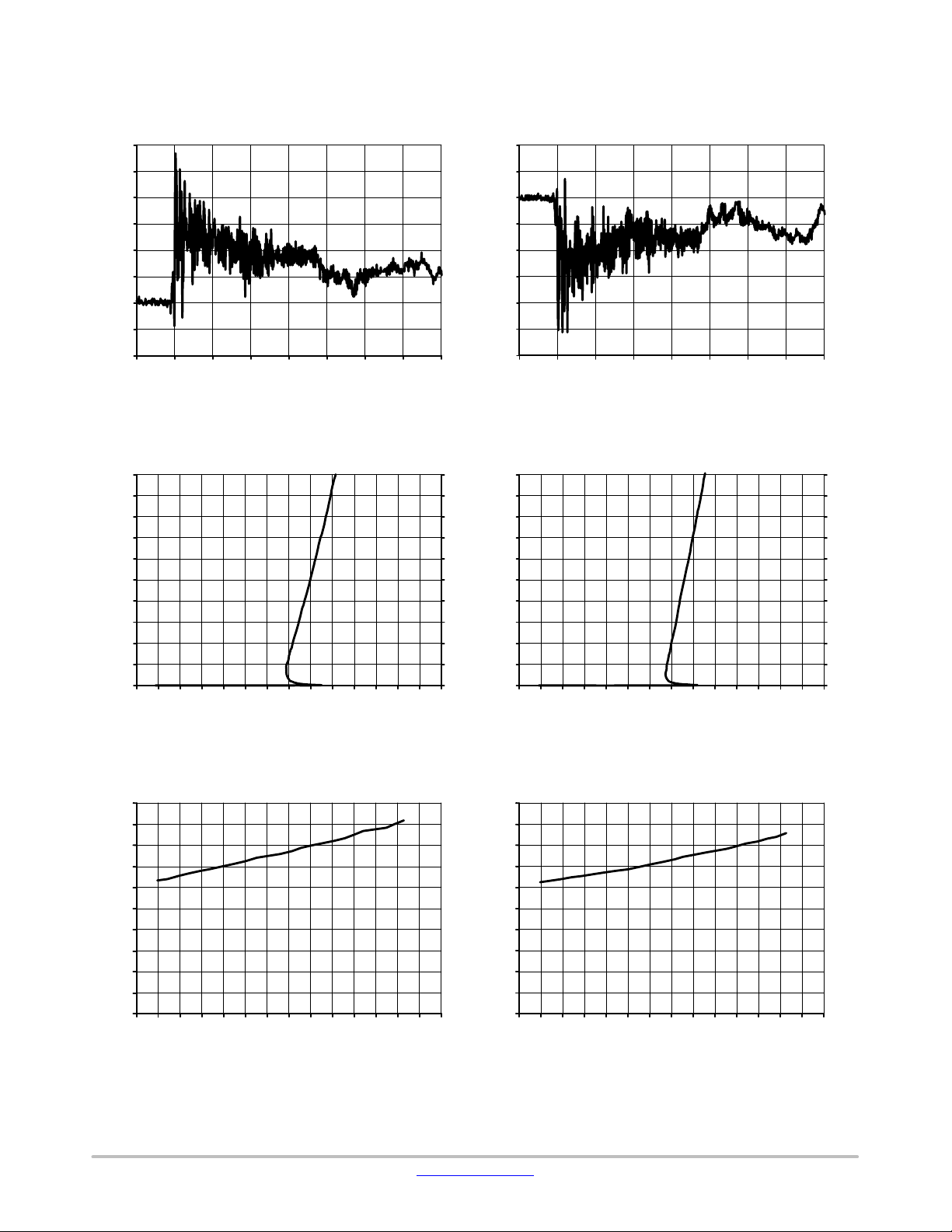
TYPICAL CHARACTERISTICS
30
25
20
15
10
Voltage (V)
5
0
−5
−10
−20
0 20 40 60 80 100 120 140
Time (ns)
Figure 1. ESD Clamping Voltage
Positive 8 kV Contact per IEC61000−4−2
20 10
18 9
16 8
14 7
12 6
(A)
10 5
TLP
I
84
63
42
21
0
0
1234567891011121314
V
(V)
CTLP
0
10
5
0
−5
−10
Voltage (V)
−15
−20
−25
−30
−20
0 20 40 60 80 100 120 140
Time (ns)
Figure 2. ESD Clamping Voltage
Negative 8 kV Contact per IEC61000−4−2
−20 10
−18 9
−16 8
−14 7
−12 6
(A)
−10 5
Eq (kV)
TLP
I
−84
IEC
V
−63
−42
−21
0
0
1234567891011121314
V
(V)
CTLP
Figure 3. Positive TLP I−V Curve Figure 4. Negative TLP I−V Curve
0
Eq (kV)
IEC
V
10
9
8
7
6
(A)
PK
5
@ I
4
C
V
3
2
1
0
0
2 4 6 8 10 12 14
135791113
IPK (A)
Figure 5. Positive Clamping Voltage vs. Peak
Pulse Current (tp = 8/20 ms)
10
9
8
7
6
(A)
PK
5
@ I
4
C
V
3
2
1
0
0
www.onsemi.com
3
2 4 6 8 10 12 14
135791113
IPK (A)
Figure 6. Negative Clamping Voltage vs. Peak
Pulse Current (tp = 8/20 ms)
Page 4

ESDM1051
TYPICAL CHARACTERISTICS
(A)
R
I
1E−03
1E−04
1E−05
1E−06
1E−07
1E−08
1E−09
1E−10
1E−11
−11
−10 −9 −8 −7 −6 −5 −4 −3 −2 −10
Figure 7. Breakdown Voltage Figure 8. Reverse Leakage Current
1234567891011
VR (V)
30
25
20
15
C (pF)
10
(A)
R
I
1E−03
1E−04
1E−05
1E−06
1E−07
1E−08
1E−09
1E−10
1E−11
1E−12
−11
−10 −9 −8 −7 −6 −5 −4 −3 −2 −10
1234567891011
VR (V)
0.0
−0.2
−0.4
−0.6
−0.8
−1.0
−1.2
−1.4
−1.6
−1.8
−2.0
S(2,1) Magnitude (dB)
−2.2
−2.4
−2.6
−2.8
−3.0
1.0E+06
5
0
−6
−5 −4 −3 −2 −10123456
V
(V)
BIAS
Figure 9. Line Capacitance, f = 1 MHz
1.0E+07 1.0E+08
Frequency (Hz)
Figure 10. Magnitude vs. Frequency
www.onsemi.com
4
Page 5

ESDM1051
IEC 61000−4−2 Spec.
Test Volt-
Level
age (kV)
1 2 7.5 4 2
2 4 15 8 4
3 6 22.5 12 6
4 8 30 16 8
First Peak
Current
(A)
Current at
30 ns (A)
Current at
60 ns (A)
Figure 11. IEC61000−4−2 Spec
Transmission Line Pulse (TLP) Measurement
Transmission Line Pulse (TLP) provides current versus
voltage (I−V) curves in which each data point is obtained
from a 100 ns long rectangular pulse from a charged
transmission line. A simplified schematic of a typical TLP
system is shown in Figure 12. TLP I−V curves of ESD
protection devices accurately demonstrate the product’s
ESD capability because the 10s of amps current levels and
under 100 ns time scale match those of an ESD event. This
is illustrated in Figure 13 where an 8 kV IEC 61000−4−2
current waveform is compared with TLP current pulses at
8 A and 16 A. A TLP I−V curve shows the voltage at which
the device turns on as well as how well the device clamps
voltage over a range of current levels.
IEC61000−4−2 Waveform
I
peak
100%
90%
I @ 30 ns
I @ 60 ns
10%
tP = 0.7 ns to 1 ns
L
Attenuator
S
50 W Coax
Cable
÷
50 W Coax
Cable
10 MW
V
C
Figure 12. Simplified Schematic of a Typical TLP
System
I
M
V
M
Oscilloscope
DUT
Figure 13. Comparison Between 8 kV IEC 61000−4−2 and 8 A and 16 A TLP Waveforms
www.onsemi.com
5
Page 6

MECHANICAL CASE OUTLINE
PACKAGE DIMENSIONS
SCALE 10:1
X4DFN2, 0.445x0.24, 0.27P
CASE 718AA
ISSUE A
DATE 21 MAR 2017
PIN 1
REFERENCE
0.03 C
0.03 C
D
TOP VIEW
SIDE VIEW
e
e/2
PIN 1
L2X
BOTTOM VIEW
A1
A
B
E
A
SEATING
C
PLANE
b
2X
2
A0.10 BC
NOTE 3
0.05
C
NOTES:
1. DIMENSIONING AND TOLERANCING PER
ASME Y14.5M, 1994.
2. CONTROLLING DIMENSION: MILLIMETERS.
3. EXPOSED COPPER ALLOWED AS SHOWN.
MILLIMETERS
DIM MIN NOM
A 0.15 0.18
A1 −−− −−−
b 0.170 0.185
D 0.415 0.445
E 0.210 0.240
e 0.270 BSC
L 0.105 0.120
MAX
0.21
0.03
0.200
0.475
0.270
0.135
GENERIC
MARKING DIAGRAMS*
X
X = Specific Device Code
*This information is generic. Please refer to
device data sheet for actual part marking.
Some products may not follow the Generic
X
Marking.
RECOMMENDED
MOUNTING FOOTPRINT*
0.27
PITCH
1
2X
0.21
2X
0.13
DIMENSIONS: MILLIMETERS
See Application Note AND8398/D for more mounting details
*For additional information on our Pb−Free strategy and soldering
details, please download the ON Semiconductor Soldering and
Mounting Techniques Reference Manual, SOLDERRM/D.
DOCUMENT NUMBER:
DESCRIPTION:
ON Semiconductor and are trademarks of Semiconductor Components Industries, LLC dba ON Semiconductor or its subsidiaries in the United States and/or other countries.
ON Semiconductor reserves the right to make changes without further notice to any products herein. ON Semiconductor makes no warranty, representation or guarantee regarding
the suitability of its products for any particular purpose, nor does ON Semiconductor assume any liability arising out of the application or use of any product or circuit, and specifically
disclaims any and all liability, including without limitation special, consequential or incidental damages. ON Semiconductor does not convey any license under its patent rights nor the
rights of others.
98AON29067G
X4DFN2, 0.445X0.24, 0.27P
Electronic versions are uncontrolled except when accessed directly from the Document Repository.
Printed versions are uncontrolled except when stamped “CONTROLLED COPY” in red.
PAGE 1 OF 1
© Semiconductor Components Industries, LLC, 2019
www.onsemi.com
Page 7

ON Semiconductor and are trademarks of Semiconductor Components Industries, LLC dba ON Semiconductor or its subsidiaries in the United States and/or other countries.
ON Semiconductor owns the rights to a number of patents, trademarks, copyrights, trade secrets, and other intellectual property. A listing of ON Semiconductor’s product/patent
coverage may be accessed at www.onsemi.com/site/pdf/Patent−Marking.pdf
ON Semiconductor makes no warranty, representation or guarantee regarding the suitability of its products for any particular purpose, nor does ON Semiconductor assume any liability
arising out of the application or use of any product or circuit, and specifically disclaims any and all liability, including without limitation special, consequential or incidental damages.
Buyer is responsible for its products and applications using ON Semiconductor products, including compliance with all laws, regulations and safety requirements or standards,
regardless of any support or applications information provided by ON Semiconductor. “Typical” parameters which may be provided in ON Semiconductor data sheets and/or
specifications can and do vary in different applications and actual performance may vary over time. All operating parameters, including “Typicals” must be validated for each customer
application by customer’s technical experts. ON Semiconductor does not convey any license under its patent rights nor the rights of others. ON Semiconductor products are not
designed, intended, or authorized for use as a critical component in life support systems or any FDA Class 3 medical devices or medical devices with a same or similar classification
in a foreign jurisdiction or any devices intended for implantation in the human body. Should Buyer purchase or use ON Semiconductor products for any such unintended or unauthorized
application, Buyer shall indemnify and hold ON Semiconductor and its officers, employees, subsidiaries, affiliates, and distributors harmless against all claims, costs, damages, and
expenses, and reasonable attorney fees arising out of, directly or indirectly, any claim of personal injury or death associated with such unintended or unauthorized use, even if such
claim alleges that ON Semiconductor was negligent regarding the design or manufacture of the part. ON Semiconductor is an Equal Opportunity/Affirmative Action Employer. This
literature is subject to all applicable copyright laws and is not for resale in any manner.
. ON Semiconductor reserves the right to make changes without further notice to any products herein.
PUBLICATION ORDERING INFORMATION
LITERATURE FULFILLMENT:
Email Requests to: orderlit@onsemi.com
ON Semiconductor Website: www.onsemi.com
TECHNICAL SUPPORT
North American Technical Support:
Voice Mail: 1 800−282−9855 Toll Free USA/Canada
Phone: 011 421 33 790 2910
Europe, Middle East and Africa Technical Support:
Phone: 00421 33 790 2910
For additional information, please contact your local Sales Representative
◊
www.onsemi.com
1
 Loading...