

Page 1
ESD8011
ESD Protection Diodes
Ultra Low Capacitance ESD Protection
Diode for High Speed Data Line
The ESD8011 ESD protection diodes are designed to protect high
speed data lines from ESD. Ultra−low capacitance and low ESD
clamping voltage make this device an ideal solution for protecting
voltage sensitive high speed data lines.
Features
• Ultra Low Capacitance (0.10 pF Typ, I/O to GND)
• Protection for the Following IEC Standards:
IEC 61000−4−2 (Level 4)
• Low ESD Clamping Voltage
• These Devices are Pb−Free, Halogen Free/BFR Free and are RoHS
Compliant
www.
onsemi.com
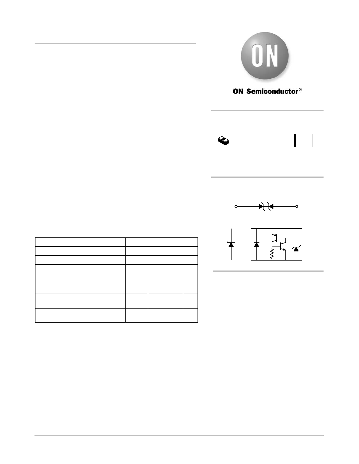
X3DFN2
CASE 152AF
R = Specific Device Code
(Rotated 90° clockwise)
M = Date Code
MARKING
DIAGRAM
PIN 1
R
M
Typical Applications
• USB 3.x
• MHL 2.0
• SATA/SAS
• PCI Express
MAXIMUM RATINGS (T
Rating Symbol Value Unit
Operating Junction Temperature Range T
Storage Temperature Range T
Lead Solder Temperature −
Maximum (10 Seconds)
IEC 61000−4−2 Contact (ESD)
IEC 61000−4−2 Air (ESD)
Maximum Peak Pulse Current
8/20 ms @ T
Maximum Peak Pulse Power
8/20 ms @ T
Stresses exceeding those listed in the Maximum Ratings table may damage the
device. If any of these limits are exceeded, device functionality should not be
assumed, damage may occur and reliability may be affected.
= 25°C
A
= 25°C
A
= 25°C unless otherwise noted)
J
J
stg
T
L
ESD
ESD
I
pp
P
pk
−55 to +125 °C
−55 to +150 °C
260 °C
±20
±20
3.6 A
34 W
kV
kV
PIN CONFIGURATION
AND SCHEMATIC
12
=
ORDERING INFORMATION
See detailed ordering and shipping information in the package
dimensions section on page 7 of this data sheet.
See Application Note AND8308/D for further description of
survivability specs.
© Semiconductor Components Industries, LLC, 2016
May, 2016 − Rev. 4
1 Publication Order Number:
ESD8011/D
Page 2

ESD8011
I
HOLD
I
I
PP
R
DYN
I
T
I
R
I
R
I
T
I
HOLD
−I
PP
DYN
V
)
HOLD
V
RWM
V
V
V
BR
C
ELECTRICAL CHARACTERISTICS
(TA = 25°C unless otherwise noted)
Symbol Parameter
V
V
V
I
HOLD
R
RWM
HOLD
I
V
Working Peak Voltage
I
Maximum Reverse Leakage Current @ V
R
Breakdown Voltage @ I
BR
I
Test Current
T
Holding Reverse Voltage
Holding Reverse Current
Dynamic Resistance
DYN
Maximum Peak Pulse Current
PP
Clamping Voltage @ I
C
VC = V
HOLD
+ (IPP * R
PP
DYN
T
)
ELECTRICAL CHARACTERISTICS (T
RWM
= 25°C unless otherwise specified)
A
V
BR
V
CVRWMVHOLD
VC = V
R
HOLD
DYN
+ (IPP * R
Parameter Symbol Conditions Min Typ Max Unit
Reverse Working Voltage V
Breakdown Voltage V
Reverse Leakage Current I
Reverse Holding Voltage V
Holding Reverse Current I
Clamping Voltage
TLP (Note 2)
RWM
HOLD
HOLD
V
I/O Pin to GND 5.5 V
IT = 1 mA, I/O Pin to GND 6.5 7.3 V
BR
V
R
= 5.5 V, I/O Pin to GND 1.0
RWM
I/O Pin to GND 2.05 V
I/O Pin to GND 17 mA
IPP = 8 A IEC61000−4−2 Level 2 Equivalent
C
11.0
(±4 kV Contact, ±8 kV Air)
IPP = 16 A
IEC61000−4−2 Level 2 Equivalent
19.0
(±8 kV Contact, ±16 kV Air)
Dynamic Resistance R
Junction Capacitance C
Series Inductance L
DYN
Pin1 to Pin2
Pin2 to Pin1
VR = 0 V, f = 1 MHz 0.10 0.20 pF
J
VR = 0 V 0.3 nH
S
1.0
1.0
Product parametric performance is indicated in the Electrical Characteristics for the listed test conditions, unless otherwise noted. Product
performance may not be indicated by the Electrical Characteristics if operated under different conditions.
1. For test procedure see Figure 5 and application note AND8307/D.
2. ANSI/ESD STM5.5.1 − Electrostatic Discharge Sensitivity Testing using Transmission Line Pulse (TLP) Model.
TLP conditions: Z
= 50 W, tp = 100 ns, tr = 4 ns, averaging window; t1 = 30 ns to t2 = 60 ns.
0
mA
V
W
www.onsemi.com
2
Page 3
ESD8011
TYPICAL CHARACTERISTICS
2
0
−2
−4
−6
(dB)
−8
−10
−12
−14
FREQUENCY (Hz)
Data Rate
Interface
USB 3.0 5 2.5 (m1) 7.5 (m2) m1 = 0.087
(Gb/s)
Fundamental Frequency
(GHz)
3rd Harmonic Frequency
(GHz)
m1
m2
3E10
1E101E91E81E7
ESD8011 Insertion Loss (dB)
m2 = 0.256
Figure 1. ESD8011 Insertion Loss
www.onsemi.com
3
Page 4

ESD8011
TYPICAL CHARACTERISTICS
20
18
16
14
12
10
8
6
TLP CURRENT (A)
4
2
0
10
V
8
IEC
, EQUIVALENT (kV)
6
4
2
610 16 2224
VC, VOLTAGE (V)
201814128420
0
Figure 2. Positive TLP I−V Curve
−20
−18
−16
−14
−12
−10
−8
−6
TLP CURRENT (A)
−4
−2
0
Figure 3. Negative TLP I−V Curve
10
V
8
IEC
, EQUIVALENT (kV)
6
4
2
610 16 2224
VC, VOLTAGE (V)
201814128420
0
www.onsemi.com
4
Page 5

ESD8011
Latch−Up Considerations
ON Semiconductor’s 8000 series of ESD protection
devices utilize a snap−back, SCR type structure. By using
this technology, the potential for a latch−up condition was
taken into account by performing load line analyses of
common high speed serial interfaces. Example load lines for
latch−up free applications and applications with the
potential for latch−up are shown below with a generic IV
characteristic of a snapback, SCR type structured device
overlaid on each. In the latch−up free load line case, the IV
characteristic of the snapback protection device intersects
the load−line in one unique point (V
I
I
SSMAX
I
OP
USB 2.0 LS/FS, USB 2.0 HS, USB 3.0 SS,
ESD8011 Latch−up free:
DisplayPort
, IOP). This is the only
OP
OP
V
DD
V
V
stable operating point of the circuit and the system is
therefore latch−up free. In the non−latch up free load line
case, the IV characteristic of the snapback protection device
, I
OPB
) and
OPA
) after a
intersects the load−line in two points (V
(V
, I
OPB
latch−up exists if the system settles at (V
). Therefore in this case, the potential for
OPB
OPB
OPA
, I
transient. Because of this, ESD8011 should not be used for
HDMI applications − ESD8104 or ESD8040 have been
designed to be acceptable for HDMI applications without
latch−up. Please refer to Application Note AND9116/D for
a more in−depth explanation of latch−up considerations
using ESD8000 series devices.
I
I
SSMAX
I
OPB
I
OPA
V
V
OPB
ESD8011 Potential Latch−up:
HDMI 1.4/1.3a TMDS
V
OPAVDD
Figure 4. Example Load Lines for Latch−up Free Applications and Applications with the Potential for Latch−up
Table 1. SUMMARY OF SCR REQUIREMENTS FOR LATCH−UP FREE APPLICATIONS
VBR (min) IH (min) VH (min) ON Semiconductor ESD8000 Series
Application
HDMI 1.4/1.3a TMDS 3.465 54.78 1.0 ESD8104, ESD8040
USB 2.0 LS/FS 3.301 1.76 1.0 ESD8004, ESD8011
USB 2.0 HS 0.482 N/A 1.0 ESD8004, ESD8011
USB 3.0 SS 2.800 N/A 1.0 ESD8004, ESD8006, ESD8011
DisplayPort 3.600 25.00 1.0 ESD8004, ESD8006, ESD8011
(V) (mA) (V) Recommended PN
www.onsemi.com
5
Page 6

ESD8011
IEC 61000−4−2 Spec.
Test Volt-
Level
age (kV)
1 2 7.5 4 2
2 4 15 8 4
3 6 22.5 12 6
4 8 30 16 8
First Peak
Current
(A)
Current at
30 ns (A)
Current at
60 ns (A)
Figure 5. IEC61000−4−2 Spec
Transmission Line Pulse (TLP) Measurement
Transmission Line Pulse (TLP) provides current versus
voltage (I−V) curves in which each data point is obtained
from a 100 ns long rectangular pulse from a charged
transmission line. A simplified schematic of a typical TLP
system is shown in Figure 6. TLP I−V curves of ESD
protection devices accurately demonstrate the product’s
ESD capability because the 10s of amps current levels and
under 100 ns time scale match those of an ESD event. This
is illustrated in Figure 7 where an 8 kV IEC 61000−4−2
current waveform is compared with TLP current pulses at
8 A and 16 A. A TLP I−V curve shows the voltage at which
the device turns on as well as how well the device clamps
voltage over a range of current levels.
IEC61000−4−2 Waveform
I
peak
100%
90%
I @ 30 ns
I @ 60 ns
10%
tP = 0.7 ns to 1 ns
L
Attenuator
S
50 W Coax
÷
50 W Coax
Cable
10 MW
V
C
Figure 6. Simplified Schematic of a Typical TLP
System
I
M
V
M
Oscilloscope
Cable
DUT
Figure 7. Comparison Between 8 kV IEC 61000−4−2 and 8 A and 16 A TLP Waveforms
www.onsemi.com
6
Page 7

ESD8011
ORDERING INFORMATION
Device Package Shipping
ESD8011MUT5G X3DFN2
(Pb−Free)
†For information on tape and reel specifications, including part orientation and tape sizes, please refer to our Tape and Reel Packaging
Specifications Brochure, BRD8011/D.
10000 / Tape & Reel
†
HDMI is a registered trademark of HDMI Licensing, LLC.
www.onsemi.com
7
Page 8

MECHANICAL CASE OUTLINE
PACKAGE DIMENSIONS
X3DFN2, 0.62x0.32, 0.355P, (0201)
SCALE 8:1
A1
2
A B
2X
E
A
C
b
0.05 BC
SEATING
PLANE
M
INDICATOR
(OPTIONAL)
2X
0.05 BC
PIN 1
0.05 C
0.05 C
L22X
M
A
BOTTOM VIEW
D
TOP VIEW
SIDE VIEW
e
1
CASE 152AF
ISSUE A
A
NOTES:
1. DIMENSIONING AND TOLERANCING PER
ASME Y14.5M, 1994.
2. CONTROLLING DIMENSION: MILLIMETERS.
MILLIMETERS
DIM MIN MAX
A 0.25 0.33
A1 −−− 0.05
b 0.22 0.28
D 0.58 0.66
E 0.28 0.36
e 0.355 BSC
L2 0.17 0.23
GENERIC
MARKING DIAGRAM*
PIN 1
XM
X = Specific Device Code
M = Date Code
RECOMMENDED
MOUNTING FOOTPRINT*
0.74
2X
0.30
DATE 17 FEB 2015
DOCUMENT NUMBER:
DESCRIPTION:
*For additional information on our Pb−Free strategy and soldering
98AON56472E
Electronic versions are uncontrolled except when accessed directly from the Document Repository.
Printed versions are uncontrolled except when stamped “CONTROLLED COPY” in red.
X3DFN2, 0.62X0.32, 0.355P, (0201)
1
2X
0.31
DIMENSIONS: MILLIMETERS
See Application Note AND8398/D for more mounting details
details, please download the ON Semiconductor Soldering and
Mounting Techniques Reference Manual, SOLDERRM/D.
PAGE 1 OF 1
ON Semiconductor and are trademarks of Semiconductor Components Industries, LLC dba ON Semiconductor or its subsidiaries in the United States and/or other countries.
ON Semiconductor reserves the right to make changes without further notice to any products herein. ON Semiconductor makes no warranty, representation or guarantee regarding
the suitability of its products for any particular purpose, nor does ON Semiconductor assume any liability arising out of the application or use of any product or circuit, and specifically
disclaims any and all liability, including without limitation special, consequential or incidental damages. ON Semiconductor does not convey any license under its patent rights nor the
rights of others.
© Semiconductor Components Industries, LLC, 2019
www.onsemi.com
Page 9

ON Semiconductor and are trademarks of Semiconductor Components Industries, LLC dba ON Semiconductor or its subsidiaries in the United States and/or other countries.
ON Semiconductor owns the rights to a number of patents, trademarks, copyrights, trade secrets, and other intellectual property. A listing of ON Semiconductor’s product/patent
coverage may be accessed at www.onsemi.com/site/pdf/Patent−Marking.pdf
ON Semiconductor makes no warranty, representation or guarantee regarding the suitability of its products for any particular purpose, nor does ON Semiconductor assume any liability
arising out of the application or use of any product or circuit, and specifically disclaims any and all liability, including without limitation special, consequential or incidental damages.
Buyer is responsible for its products and applications using ON Semiconductor products, including compliance with all laws, regulations and safety requirements or standards,
regardless of any support or applications information provided by ON Semiconductor. “Typical” parameters which may be provided in ON Semiconductor data sheets and/or
specifications can and do vary in different applications and actual performance may vary over time. All operating parameters, including “Typicals” must be validated for each customer
application by customer’s technical experts. ON Semiconductor does not convey any license under its patent rights nor the rights of others. ON Semiconductor products are not
designed, intended, or authorized for use as a critical component in life support systems or any FDA Class 3 medical devices or medical devices with a same or similar classification
in a foreign jurisdiction or any devices intended for implantation in the human body. Should Buyer purchase or use ON Semiconductor products for any such unintended or unauthorized
application, Buyer shall indemnify and hold ON Semiconductor and its officers, employees, subsidiaries, affiliates, and distributors harmless against all claims, costs, damages, and
expenses, and reasonable attorney fees arising out of, directly or indirectly, any claim of personal injury or death associated with such unintended or unauthorized use, even if such
claim alleges that ON Semiconductor was negligent regarding the design or manufacture of the part. ON Semiconductor is an Equal Opportunity/Affirmative Action Employer. This
literature is subject to all applicable copyright laws and is not for resale in any manner.
. ON Semiconductor reserves the right to make changes without further notice to any products herein.
PUBLICATION ORDERING INFORMATION
LITERATURE FULFILLMENT:
Email Requests to: orderlit@onsemi.com
ON Semiconductor Website: www.onsemi.com
TECHNICAL SUPPORT
North American Technical Support:
Voice Mail: 1 800−282−9855 Toll Free USA/Canada
Phone: 011 421 33 790 2910
Europe, Middle East and Africa Technical Support:
Phone: 00421 33 790 2910
For additional information, please contact your local Sales Representative
◊
www.onsemi.com
1
 Loading...