

Page 1
ESD7484
ESD Protection Diode
4−Line, Ultra Large Bandwidth
Functional Description
The ESD7484 chip is a monolithic, application specific discrete
device dedicated to ESD protection of the HDMI connection. It also
offers the same high level of protection for IEEE 1394a and IEEE
1394b/c, USB2.0, Ethernet links, and video lines.
Its ultra high cutoff frequency (5.3 GHz) secures a high level of
signal integrity. The device topology provides this integrity without
compromising the complete protection of ICs against the most
stringent ESD strikes.
Features
• Wideband Performance
• Flow−Through Layout
• Low Profile with Small Footprint: 1.6 mm x 1.1 mm Package
• 0.4 mm Pitch WLCSP Package
• IEC61000−4−2 Level 4 (At External Pins)
♦ ± 15 kV (Air Discharge)
♦ ± 15 kV (Contact Discharge)
• These Devices are Pb−Free, Halogen Free and are RoHS II
Compliant
www.onsemi.com
MARKING
DIAGRAM
84
WLCSP10
CASE 567DE
84 = Specific Device Code
Y = Year
W = Work Week
G = Pb−Free Package
YW
G
ORDERING INFORMATION
See detailed ordering and shipping information in the package
dimensions section on page 6 of this data sheet.
Applications
• Mobile Phones and Communications Systems
• HDMI Ports at 1.65 Gb/s and up to 3.2 Gb/s
• Video Out Protection
A
B
C
External
(Connector)
D
E
F
Figure 1. Pin Configuration (Bump View)
123
_1+
OUT
GND
D
_1−
OUT
_2+
OUT
GND
_2−
OUT
DIN_1+D
D
_1−
IN
Internal
(ASIC)
_2+D
D
IN
DIN_2−D
© Semiconductor Components Industries, LLC, 2011
November, 2017 − Rev. 1
1 Publication Order Number:
ESD7484/D
Page 2
ESD7484
ABSOLUTE MAXIMUM RATINGS
Symbol Parameter Value Unit
V
P
T
Stresses exceeding those listed in the Maximum Ratings table may damage the device. If any of these limits are exceeded, device functionality
should not be assumed, damage may occur and reliability may be affected.
ELECTRICAL CHARACTERISTICS (Note 1)
Symbol Test Condition Min Typ Max Unit
V
I
C
DC
1. All parameters specified at TA = 25°C unless otherwise noted.
2. Standard IEC 61000−4−2 with C
ESD IEC61000−4−2, level 4 – air discharge (external pins)
PP
ESD IEC61000−4−2, level 4 – contact discharge (external pins)
Peak Pulse Power Dissipation (8/20 ms)
PP
T
Maximum Junction Temperature 125 °C
J
Storage Temperature Range −55 to +150 °C
stg
BR
RM
line
I/O−I/O
Breakdown Voltage (Ir = 1 mA) 6 9 V
Leakage Current @ Vrm (Vrm = 3 V per line) 3 100 nA
V
line
V
line
V
line
= 0 V, V
= 0 V, V
= 0 V, V
= 30 mV, F = 1 MHz, Capacitor between I/O and GND 1.6 1.75
osc
= 30 mV, F = 1 MHz, Capacitor between I/O 0.8
osc
= 30 mV, F = 1 MHz, Capacitance Variation between I/O 0.006 pF
osc
Discharge
= 150 pF, R
Discharge
= 330 W.
±15
±15
70 W
kV
pF
www.onsemi.com
2
Page 3
ESD7484
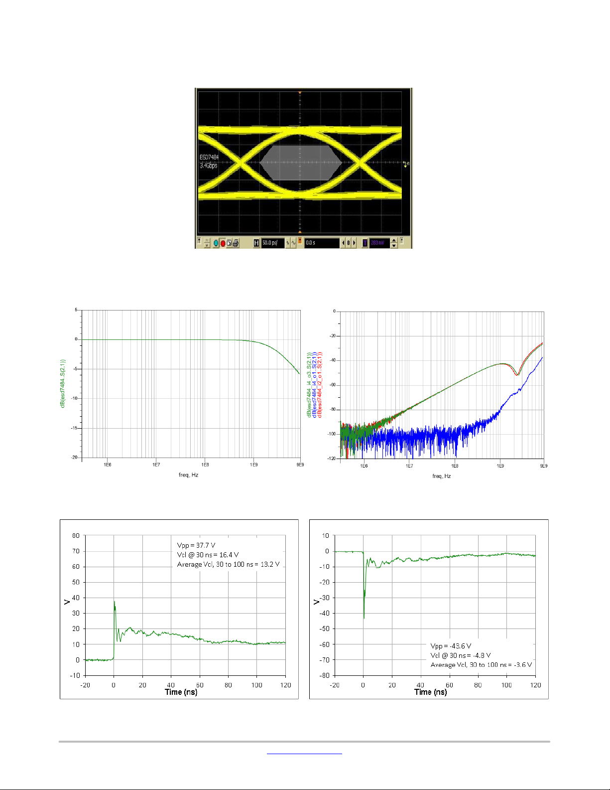
TYPICAL CHARACTERISTICS
Figure 2. HDMI1.4 Test Conditions
3.4 Gb/s Datarate;
Clears HDMI Source Mask
Figure 3. S21 Plot Figure 4. Crosstalk Measurements
Figure 5. ESD Clamping Voltage Screenshot
Positive 8 kV Contact per IEC61000−4−2
Figure 6. ESD Clamping Voltage Screenshot
Negative 8 kV Contact per IEC61000−4−2
www.onsemi.com
3
Page 4

ESD7484
IEC61000−4−2 Spec.
Test Volt-
Level
age (kV)
1 2 7.5 4 2
2 4 15 8 4
3 6 22.5 12 6
4 8 30 16 8
ESD Gun
First Peak
Current
(A)
Current at
30 ns (A)
Device
Under
Test
50 W
Cable
IEC61000−4−2 Waveform
I
peak
Current at
60 ns (A)
100%
90%
I @ 30 ns
I @ 60 ns
10%
Figure 7. IEC61000−4−2 Spec
Oscilloscope
50 W
tP = 0.7 ns to 1 ns
Figure 8. Diagram of ESD Clamping Voltage Test Setup
The following is taken from Application Note
AND8308/D − Interpretation of Datasheet Parameters
for ESD Devices.
ESD Voltage Clamping
For sensitive circuit elements it is important to limit the
voltage that an IC will be exposed to during an ESD event
to as low a voltage as possible. The ESD clamping voltage
is the voltage drop across the ESD protection diode during
an ESD event per the IEC61000−4−2 waveform. Since the
IEC61000−4−2 was written as a pass/fail spec for larger
100
t
r
90
80
70
60
50
40
30
20
% OF PEAK PULSE CURRENT
10
0
020406080
PEAK VALUE I
t
P
Figure 9. 8 x 20 ms Pulse Waveform
systems such as cell phones or laptop computers it is not
clearly defined in the spec how to specify a clamping voltage
at the device level. ON Semiconductor has developed a way
to examine the entire voltage waveform across the ESD
protection diode over the time domain of an ESD pulse in the
form of an oscilloscope screenshot, which can be found on
the datasheets for all ESD protection diodes. For more
information on how ON Semiconductor creates these
screenshots and how to interpret them please refer to
AND8307/D.
@ 8 ms
RSM
PULSE WIDTH (tP) IS DEFINED
AS THAT POINT WHERE THE
PEAK CURRENT DECAY = 8 ms
HALF VALUE I
t, TIME (ms)
/2 @ 20 ms
RSM
www.onsemi.com
4
Page 5

ESD7484
Figure 10. Positive TLP I−V Curve Figure 11. Negative TLP I−V Curve
Transmission Line Pulse (TLP) Measurement
Transmission Line Pulse (TLP) provides current versus
voltage (I−V) curves in which each data point is obtained
from a 100 ns long rectangular pulse from a charged
transmission line. A simplified schematic of a typical TLP
system is shown in Figure 12. TLP I−V curves of ESD
protection devices accurately demonstrate the product’s
ESD capability because the 10s of amps current levels and
under 100 ns time scale match those of an ESD event. This
is illustrated in Figure 13 where an 8 kV IEC61000−4−2
current waveform is compared with TLP current pulses at
8 A and 16 A. A TLP I−V curve shows the voltage at which
the device turns on as well as how well the device clamps
voltage over a range of current levels. A typical TLP I−V
curve for the ESD7383 is shown in Figures 10 and 11.
L
Attenuator
S
50 W Coax
Cable
÷
50 W Coax
Cable
Figure 12. Simplified Schematic of a Typical TLP
10 MW
V
C
System
I
M
V
M
Oscilloscope
DUT
Figure 13. Comparison Between 8 kV IEC61000−4−2 and 8 A and 16 A TLP Waveforms
www.onsemi.com
5
Page 6

ESD7484
TYPICAL APPLICATION SCHEMATIC
HDMI Type C
Connector
Data2 Shield
Data2 +
Data2 −
Data1 Shield
Data1 +
Data1 −
Data0 Shield
Data0 +
Data0 −
CLK Shield
CLK +
CLK −
DDC GROUND
Reserved
+5 Power
CEC
SCL
SDA
HPD
ESD7484
1
2
3
4
5
6
7
8
9
10
11
12
13
14
15
16
17
18
19
A1A3C1 D1 F1C3 D3 F 3B2 E2
A1 A3
5V
B2, C2
C3 B3
HPD SDA SCL CEC
100KW
A1A3 C1 D1 F 1C3 D3 F 3B2 E2
A2
1.75KW
27KW
1.75KW
ESD7484
C1
B1
Data2 +
Data2 −
Data1 +
Data1 −
Data0 +
Data0 −
CLK +
CLK −
CEC
SCL
SDA
+5 Power
HPD
5V
VDD_CEC
ESD5384
Figure 14. Typical Application Schematic
ORDERING INFORMATION
Pocket Size (mm)
X A0 X K
Part Number Chip Size (mm)
ESD7484 1.6 x 1.1 x 0.615 1.80 x 1.27 x 0.73 4 mm 4 mm WLCSP10
B
0
P0P
0
Package Shipping
1
5000 / Tape & Reel
(Pb−Free)
†For information on tape and reel specifications, including part orientation and tape sizes, please refer to our Tape and Reel Packaging
Specifications Brochure, BRD8011/D.
†
www.onsemi.com
6
Page 7

MECHANICAL CASE OUTLINE
PACKAGE DIMENSIONS
SCALE 4:1
WLCSP10, 1.60x1.10
CASE 567DE−01
ISSUE O
DATE 10 MAY 2011
REFERENCE
2X
2X
NOTE 3
0.03
PIN A1
0.05 C
10X
A0.05 BC
C
0.05 C
0.05 C
0.05 C
A1
b
D
TOP VIEW
SIDE VIEW
eD
1
2
3
ABC
DEF
BOTTOM VIEW
eD/2
A
A2
A
eE
B
E
C
SEATING
PLANE
NOTES:
1. DIMENSIONING AND TOLERANCING PER
ASME Y14.5M, 1994.
2. CONTROLLING DIMENSION: MILLIMETERS.
3. COPLANARITY APPLIES TO SPHERICAL
CROWNS OF SOLDER BALLS.
MILLIMETERS
DIMAMIN MAX
A1
A2 0.41 REF
b 0.24 0.29
D 1.60 BSC
E
eD 0.400 BSC
eE 0.347 BSC
0.63
0.57
0.17 0.24
1.10 BSC
GENERIC
MARKING DIAGRAM*
XX
YW
G
Y = Year
W = Work Week
G = Pb−Free Package
*This information is generic. Please refer to
device data sheet for actual part marking.
Pb−Free indicator, “G” or microdot “ G”,
may or may not be present.
RECOMMENDED
SOLDERING FOOTPRINT*
0.40
PITCH
0.35
PITCH
A1
*For additional information on our Pb−Free strategy and soldering
details, please download the ON Semiconductor Soldering and
Mounting Techniques Reference Manual, SOLDERRM/D.
DOCUMENT NUMBER:
DESCRIPTION:
98AON57139E
WLCSP10, 1.60X1.10
0.20
PITCH
10X
DIMENSIONS: MILLIMETERS
PACKAGE
OUTLINE
0.25
Electronic versions are uncontrolled except when accessed directly from the Document Repository.
Printed versions are uncontrolled except when stamped “CONTROLLED COPY” in red.
PAGE 1 OF 1
ON Semiconductor and are trademarks of Semiconductor Components Industries, LLC dba ON Semiconductor or its subsidiaries in the United States and/or other countries.
ON Semiconductor reserves the right to make changes without further notice to any products herein. ON Semiconductor makes no warranty, representation or guarantee regarding
the suitability of its products for any particular purpose, nor does ON Semiconductor assume any liability arising out of the application or use of any product or circuit, and specifically
disclaims any and all liability, including without limitation special, consequential or incidental damages. ON Semiconductor does not convey any license under its patent rights nor the
rights of others.
© Semiconductor Components Industries, LLC, 2019
www.onsemi.com
Page 8

ON Semiconductor and are trademarks of Semiconductor Components Industries, LLC dba ON Semiconductor or its subsidiaries in the United States and/or other countries.
ON Semiconductor owns the rights to a number of patents, trademarks, copyrights, trade secrets, and other intellectual property. A listing of ON Semiconductor’s product/patent
coverage may be accessed at www.onsemi.com/site/pdf/Patent−Marking.pdf
ON Semiconductor makes no warranty, representation or guarantee regarding the suitability of its products for any particular purpose, nor does ON Semiconductor assume any liability
arising out of the application or use of any product or circuit, and specifically disclaims any and all liability, including without limitation special, consequential or incidental damages.
Buyer is responsible for its products and applications using ON Semiconductor products, including compliance with all laws, regulations and safety requirements or standards,
regardless of any support or applications information provided by ON Semiconductor. “Typical” parameters which may be provided in ON Semiconductor data sheets and/or
specifications can and do vary in different applications and actual performance may vary over time. All operating parameters, including “Typicals” must be validated for each customer
application by customer’s technical experts. ON Semiconductor does not convey any license under its patent rights nor the rights of others. ON Semiconductor products are not
designed, intended, or authorized for use as a critical component in life support systems or any FDA Class 3 medical devices or medical devices with a same or similar classification
in a foreign jurisdiction or any devices intended for implantation in the human body. Should Buyer purchase or use ON Semiconductor products for any such unintended or unauthorized
application, Buyer shall indemnify and hold ON Semiconductor and its officers, employees, subsidiaries, affiliates, and distributors harmless against all claims, costs, damages, and
expenses, and reasonable attorney fees arising out of, directly or indirectly, any claim of personal injury or death associated with such unintended or unauthorized use, even if such
claim alleges that ON Semiconductor was negligent regarding the design or manufacture of the part. ON Semiconductor is an Equal Opportunity/Affirmative Action Employer. This
literature is subject to all applicable copyright laws and is not for resale in any manner.
. ON Semiconductor reserves the right to make changes without further notice to any products herein.
PUBLICATION ORDERING INFORMATION
LITERATURE FULFILLMENT:
Email Requests to: orderlit@onsemi.com
ON Semiconductor Website: www.onsemi.com
TECHNICAL SUPPORT
North American Technical Support:
Voice Mail: 1 800−282−9855 Toll Free USA/Canada
Phone: 011 421 33 790 2910
Europe, Middle East and Africa Technical Support:
Phone: 00421 33 790 2910
For additional information, please contact your local Sales Representative
◊
www.onsemi.com
1
 Loading...