

Page 1

Is Now Part of
To learn more about ON Semiconductor, please visit our website at
www.onsemi.com
Please note: As part of the Fairchild Semiconductor integration, some of the Fairchild orderable part numbers
will need to change in order to meet ON Semiconductor’s system requirements. Since the ON Semiconductor
product management systems do not have the ability to manage part nomenclature that utilizes an underscore
(_), the underscore (_) in the Fairchild part numbers will be changed to a dash (-). This document may contain
device numbers with an underscore (_). Please check the ON Semiconductor website to verify the updated
device numbers. The most current and up-to-date ordering information can be found at www.onsemi.com. Please
email any questions regarding the system integration to Fairchild_questions@onsemi.com.
ON Semi conductor an d the ON Semico nductor logo a re trademar ks of Semicon ductor Comp onents Indus tries, L LC dba ON Semico nductor or it s subsidiari es in the United S tates and /or other coun tries. ON Se miconducto r owns the righ ts to a number
of patents, trademarks, copyrights, trade secrets, and other intellectual property. A listing of ON Semiconductor’s product/patent coverage may be accessed at www.onsemi.com/site/pdf/Patent-Marking.pdf. ON Semiconductor reserve s the right
to make changes without f urther noti ce to any produc ts herein. ON S emicon ductor makes no warran ty, representat ion or guar antee regar ding the suitability of its pro ducts for any partic ular purpose, n or does ON Semic onductor as sume any liabilit y
arisin g out of the applica tion or us e of any product o r circui t, and specific ally dis claims any and all lia bilit y, includin g witho ut limit ation sp ecial, c onsequential or incidental da mages . Buye r is responsib le for it s products and a pplica tions us ing ON
Semic onductor pr oducts, inc luding complia nce with all law s, regulati ons and safet y requirem ents or stan dards, rega rdless of an y support or ap plications in formation p rovided by ON S emiconduc tor. “Typical ” parameter s which may be pr ovided in ON
Semic onductor data s heet s and/or s pecificatio ns can and do vary in diff erent a pplica tions an d actual perf ormance may var y over time. All o perat ing parameter s, including “Typical s” must b e validated for e ach cus tomer ap plicat ion by customer’s
techni cal exper ts. ON Semic onductor do es not conve y any license un der its pate nt rights no r the rights o f others. ON S emiconduc tor produc ts are not des igned, inte nded, or autho rized for use a s a critical c omponent in lif e support s ystems or an y FDA
Clas s 3 medical devi ces or medica l devices wit h a same or similar c lassificat ion in a foreign j urisdictio n or any device s intended for im plantation in t he human body. Sho uld Buyer pur chase or use ON S emiconduct or products f or any such unint ended
or unaut horized appli cation, Buy er shall indemn ify and hold O N Semiconduc tor and its of ficers, e mployees , subsidiari es, affilia tes, and dis tributor s harmless ag ainst all claim s, costs , damages, an d expenses , and reason able attorn ey fees aris ing out
of, dire ctly or indire ctly, any claim o f personal inj ury or death as sociated w ith such unint ended or unauth orized use, e ven if such claim a lleges that ON S emiconduc tor was neglig ent regardin g the design or ma nufacture o f the part. ON S emiconduct or
is an Equa l Oppor tunity/Affirm ative Action E mployer. This li terature is s ubject to all applicable c opyright la ws and is no t for resale in any manner.
Page 2
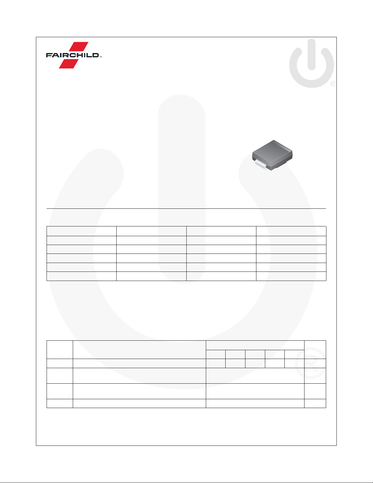
ES3A - ES3J
Fast Rectifiers
Features
• For Surface Mount Applications
• Glass-Passivated Junction
• Low-Profile Package
• Easy Pick and Place
• Built-in Strain Relief
• Superfast Recovery Times for High Efficiency
ES3A - ES3J — Fast Rectifiers
June 2016
SMC/DO-214AB
COLOR BAND DENOTES CATHODE
Ordering Information
Part Number Top Mark Package Packing Method
ES3A ES3A DO-214AB (SMC) Tape and Reel
ES3B ES3B DO-214AB (SMC) Tape and Reel
ES3C ES3C DO-214AB (SMC) Tape and Reel
ES3D ES3D DO-214AB (SMC) Tape and Reel
ES3J ES3J DO-214AB (SMC) Tape and Reel
Absolute Maximum Ratings
Stresses exceeding the absolute maximum ratings may damage the device. The device may not function or be operable above the recommended operating co nd iti ons an d s tres si ng the parts to these levels is not recommended. In addition, extended exposure to stresses above the recommended operating conditions may affect device reliability. The
absolute maximum ratings are stress ratings only. Values are at T
Symbol Parameter
V
I
F(AV)
I
FSM
T
J, TSTG
Maximum Repetitive Reverse Voltage 50 100 150 200 600 V
RRM
Average Rectified Forward Current,
.375” Lead Length at T
Non-Repetitive Peak Forward Surge Current
8.3 ms Single Half-Sine Wave
Operating Junction and Storage Temperature Range -50 to +150 C
= 75°C
A
= 25°C unless otherwise noted.
A
Value
ES3A ES3B ES3C ES3D ES3J
3.0 A
100 A
Unit
© 1999 Fairchild Semiconductor Corporation www.fairchildsemi.com
ES3A - ES3J Rev. 2.11
Page 3
Thermal Characteristics
Values are at TA = 25°C unless otherwise noted.
Symbol Parameter Value Unit
P
Power Dissipation 1.66 W
D
R
R
Thermal Resistance,
JA
Junction to Ambient
Thermal Resistance,
JL
Junction to Lead
(1)
(1)
Note:
1. Device mounted on FR-4 PCB 0.013 mm.
Maximum Land Pattern: 16 x 16 mm 47
Minimum Land Pattern: 2.6 x 3.2 mm 125
Maximum Land Pattern: 16 x 16 mm 12
Minimum Land Pattern: 2.6 x 3.2 mm 16
C/W
C/W
Electrical Characteristics
Values are at TA = 25°C unless otherwise noted.
ES3A - ES3J — Fast Rectifiers
Symbol Parameter Conditions
Maximum Forward Voltage IF = 3.0 A 0.95 1.70 V
V
F
I
= 0.5 A,
Reverse Recovery Time
t
rr
Maximum Reverse Current
I
R
at Rated V
Total Capacitance VR = 4.0 V, f = 1.0 MHz 45 pF
C
T
R
F
= 1.0 A,
I
R
= 0.25 A
I
RR
TA = 25C10
T
= 100C500
A
Typ. 20 35
Max. 30 45
Value
ES3A ES3B ES3C ES3D ES3J
Unit
ns
A
© 1999 Fairchild Semiconductor Corporation www.fairchildsemi.com
ES3A - ES3J Rev. 2.11 2
Page 4

Typical Performance Characteristics
0 25 50 75 100 125 150 175
0
0.5
1
1.5
2
2.5
3
3.5
Ambient Temperature [ºC]
Average Rectified Forward Current, I
F
[A]
SINGLE PHASE
HALF WAVE
60HZ
RESISTIVE OR
INDUCTIVE LOAD
.375" (9.0mm) LEAD
LENGTHS
0.01
0.1
1
10
100
0.40.60.81.01.21.41.61.8
ES3A-ES3D
ES3J
TA=25 oC
Pulse Width = 300us
2% Duty Cycle
Forward Voltage Drop, VF[V]
Forward Current, I
F
[A]
0.1 0.5 1 5 10 20 50 100 500
0
10
20
30
40
50
60
70
80
90
100
Reverse Voltage, VR [V]
Total Capacitance, C
T
[pF]
0 20406080100120140
0.1
1
10
100
1000
Percent of Rated Peak Reverse Voltage [%]
Reverse Current, I
R
[ A]
T = 25 C
º
A
T = 100 C
º
A
T = 75 C
º
A
μ
Pulse
Generator
(Note 2)
50
NONINDUCTIVE
50
NONINDUCTIVE
DUT
(-)
(+)
OSCILLOSCOPE
(Note 1)
50
NONINDUCTIVE
50V
(approx)
1. Rise time = 7.0 ns max; Input impedance = 1.0 megaohm 22 pf.
2. Rise time = 10 ns max; Source impedance = 50 ohms.
NOTES:
trr
+0.5A
0
-0.25A
-1.0A
Figure 1. Forward Current Derating Curve Figure 2. Foward Voltage Characteristics
ES3A - ES3J — Fast Rectifiers
© 1999 Fairchild Semiconductor Corporation www.fairchildsemi.com
ES3A - ES3J Rev. 2.11 3
Figure 3. Total Capacitance
Figure 4. Reverse Current vs. Reverse Voltage
1.0cm S ET TIME BASE FOR
Figure 5. Reverse Recovery Time Characteristic and Test Circuit Diagram
5/ 10 ns/ cm
Page 5

B
8.15
7.75
1.96
2.45
1.90
6.25
5.55
A
0.30
0.05
NOTES:
7.15
6.60
TOP VIEW
A
4.70
4.40
SIDE VIEW
3.27
2.75
B
3.39
6.81
M
0.13
2.65 MAX
C
B A
LAND PATTERN RECOMMENDATION
8°
R0.15
0°
4X
GAGE
C
PLANE
0.41
0.15
SEATING
PLANE
0.203
0.050
0.13
M
C
B
B A
0.45
1.60
0.75
8°
0°
DETAIL A
SCALE 2:1
EXCEPT WHERE NOTED, CONFORMS TO
A.
JEDEC DO-214, VARIATION AB
B
DOES NOT COMPLY TO JEDEC STD. VALUE
C. ALL DIMENSIONS ARE IN MILLIMETERS
D. DIMENSIONS ARE EXCLUSIVE OF BURRS,
MOLD FLASH, AND TIE BAR PROTRUSIONS.
E. DIMENSIONS AND TOLERANCING AS PER
ASME Y14.5-2009
F. LAND PATTERN STANDARD: DIOM7957X241M
G. DRAWING FILENAME: MKT-DO214ABrev2
Page 6

ON Semiconductor and are trademarks of Semiconductor Components Industries, LLC dba ON Semiconductor or its subsidiaries in the United States and/or other countries.
ON Semiconductor owns the rights to a number of patents, trademarks, copyrights, trade secrets, and other intellectual property. A listing of ON Semiconductor’s product/patent
coverage may be accessed at www.onsemi.com/site/pdf/Patent−Marking.pdf
ON Semiconductor makes no warranty, representation or guarantee regarding the suitability of its products for any particular purpose, nor does ON Semiconductor assume any liability
arising out of the application or use of any product or circuit, and specifically disclaims any and all liability, including without limitation special, consequential or incidental damages.
Buyer is responsible for its products and applications using ON Semiconductor products, including compliance with all laws, regulations and safety requirements or standards,
regardless of any support or applications information provided by ON Semiconductor. “Typical” parameters which may be provided in ON Semiconductor data sheets and/or
specifications can and do vary in different applications and actual performance may vary over time. All operating parameters, including “Typicals” must be validated for each customer
application by customer’s technical experts. ON Semiconductor does not convey any license under its patent rights nor the rights of others. ON Semiconductor products are not
designed, intended, or authorized for use as a critical component in life support systems or any FDA Class 3 medical devices or medical devices with a same or similar classification
in a foreign jurisdiction or any devices intended for implantation in the human body. Should Buyer purchase or use ON Semiconductor products for any such unintended or unauthorized
application, Buyer shall indemnify and hold ON Semiconductor and its officers, employees, subsidiaries, affiliates, and distributors harmless against all claims, costs, damages, and
expenses, and reasonable attorney fees arising out of, directly or indirectly, any claim of personal injury or death associated with such unintended or unauthorized use, even if such
claim alleges that ON Semiconductor was negligent regarding the design or manufacture of the part. ON Semiconductor is an Equal Opportunity/Affirmative Action Employer. This
literature is subject to all applicable copyright laws and is not for resale in any manner.
. ON Semiconductor reserves the right to make changes without further notice to any products herein.
PUBLICATION ORDERING INFORMATION
LITERATURE FULFILLMENT:
Literature Distribution Center for ON Semiconductor
19521 E. 32nd Pkwy, Aurora, Colorado 80011 USA
Phone: 303−675−2175 or 800−344−3860 Toll Free USA/Canada
Fax: 303−675−2176 or 800−344−3867 Toll Free USA/Canada
Email: orderlit@onsemi.com
© Semiconductor Components Industries, LLC
N. American Technical Support: 800−282−9855 Toll Free
USA/Canada
Europe, Middle East and Africa Technical Support:
Phone: 421 33 790 2910
Japan Customer Focus Center
Phone: 81−3−5817−1050
www.onsemi.com
ON Semiconductor Website: www.onsemi.com
Order Literature: http://www.onsemi.com/orderlit
For additional information, please contact your local
Sales Representative
www.onsemi.com
1
Page 7

Mouser Electronics
Authorized Distributor
Click to View Pricing, Inventory, Delivery & Lifecycle Information:
ON Semiconductor:
ES3J
 Loading...