

Page 1
MUN2114, MMUN2114L,
MUN5114, DTA114YE,
DTA114YM3, NSBA114YF3
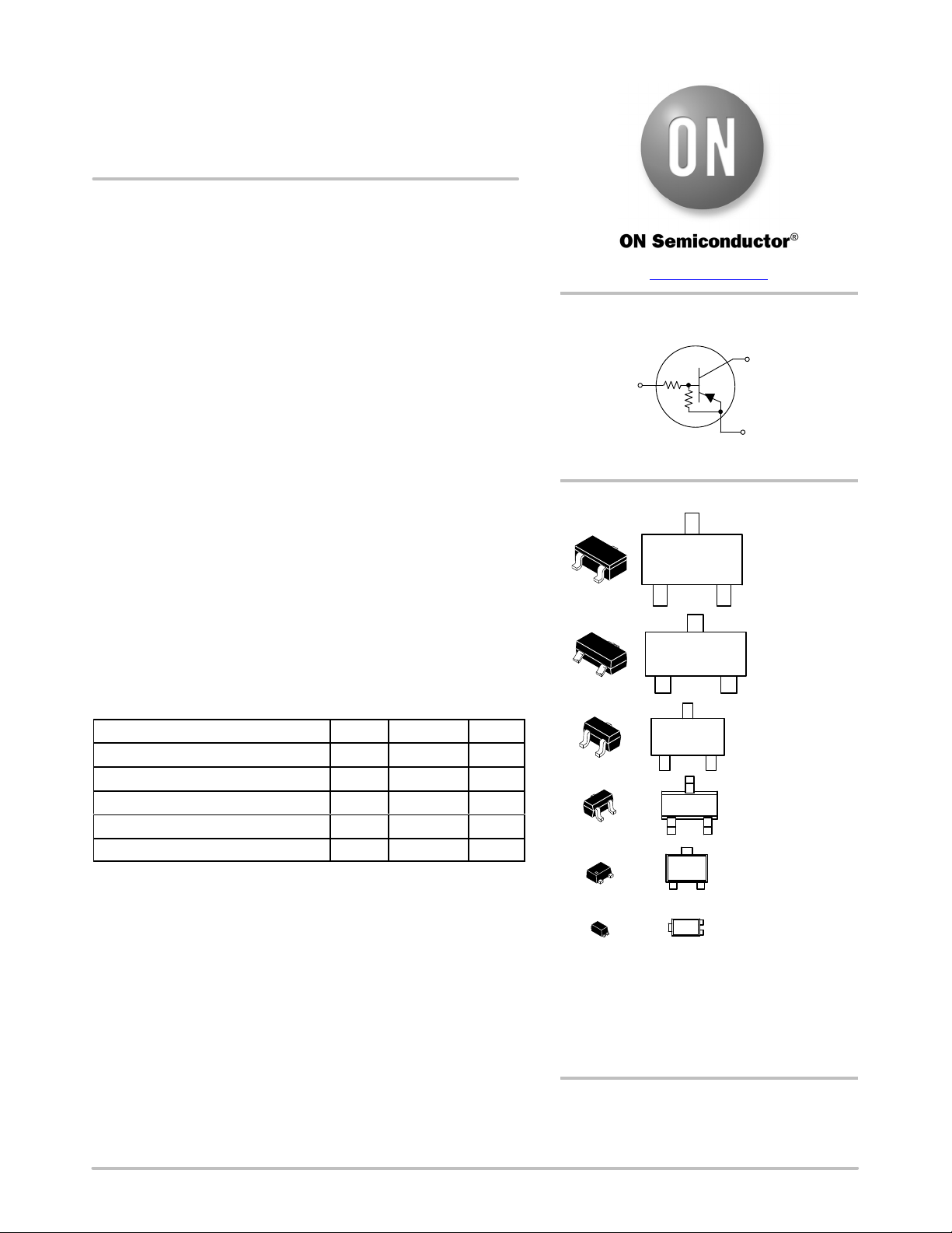
Digital Transistors (BRT)
R1 = 10 kW, R2 = 47 kW
PNP Transistors with Monolithic Bias
Resistor Network
This series of digital transistors is designed to replace a single
device and its external resistor bias network. The Bias Resistor
Transistor (BRT) contains a single transistor with a monolithic bias
network consisting of two resistors; a series base resistor and a
base−emitter resistor. The BRT eliminates these individual
components by integrating them into a single device. The use of a BRT
can reduce both system cost and board space.
PIN 1
BASE
(INPUT)
www.onsemi.com
PIN CONNECTIONS
COLLECTOR
R1
R2
(OUTPUT)
PIN 2
EMITTER
(GROUND)
PIN 3
Features
• Simplifies Circuit Design
• Reduces Board Space
• Reduces Component Count
• S and NSV Prefix for Automotive and Other Applications Requiring
Unique Site and Control Change Requirements; AEC−Q101
Qualified and PPAP Capable
• These Devices are Pb−Free, Halogen Free/BFR Free and are RoHS
Compliant
MAXIMUM RATINGS (T
Rating
Collector−Base Voltage V
Collector−Emitter Voltage V
Collector Current − Continuous I
Input Forward Voltage V
Input Reverse Voltage V
Stresses exceeding those listed in the Maximum Ratings table may damage the
device. If any of these limits are exceeded, device functionality should not be
assumed, damage may occur and reliability may be affected.
= 25°C)
A
Symbol Max Unit
CBO
CEO
C
IN(fwd)
IN(rev)
50 Vdc
50 Vdc
100 mAdc
40 Vdc
6 Vdc
MARKING DIAGRAMS
XX MG
G
1
XXX MG
G
1
XX MG
G
1
XX M
1
XX M
1
X M
1
CASE 318D
STYLE 1
SOT−23
CASE 318
STYLE 6
SC−70/SOT−323
CASE 419
STYLE 3
CASE 463
STYLE 1
SOT−723
CASE 631AA
STYLE 1
SOT−1123
CASE 524AA
STYLE 1
SC−59
SC−75
© Semiconductor Components Industries, LLC, 2012
October, 2016 − Rev. 6
XXX = Specific Device Code
M = Date Code*
G =Pb−Free Package
(Note: Microdot may be in either location)
*Date Code orientation may vary depending up-
on manufacturing location.
ORDERING INFORMATION
See detailed ordering, marking, and shipping information in
the package dimensions section on page 2 of this data sheet.
1 Publication Order Number:
DTA114Y/D
Page 2
MUN2114, MMUN2114L, MUN5114, DTA114YE, DTA114YM3, NSBA114YF3
Table 1. ORDERING INFORMATION
Device Part Marking Package Shipping
MUN2114T1G, SMUN2114T1G* 6D SC−59 3,000 / Tape & Reel
MMUN2114LT1G, SMMUN2114LT1G* A6D SOT−23 3,000 / Tape & Reel
MMUN2114LT3G, NSVMMUN2114LT3G* A6D SOT−23 10,000 / Tape & Reel
MUN5114T1G, SMUN5114T1G* 6D SC−70/SOT−323 3,000 / Tape & Reel
SMUN5114T3G 6D SC−70/SOT−323 10,000 / Tape & Reel
DTA114YET1G, SDTA114YET1G* 6D SC−75 3,000 / Tape & Reel
DTA114YM3T5G, NSVDTA114YM3T5G* 6D SOT−723 8,000 / Tape & Reel
NSBA114YF3T5G K SOT−1123 8,000 / Tape & Reel
†For information on tape and reel specifications, including part orientation and tape sizes, please refer to our Tape and Reel Packaging
Specifications Brochure, BRD8011/D.
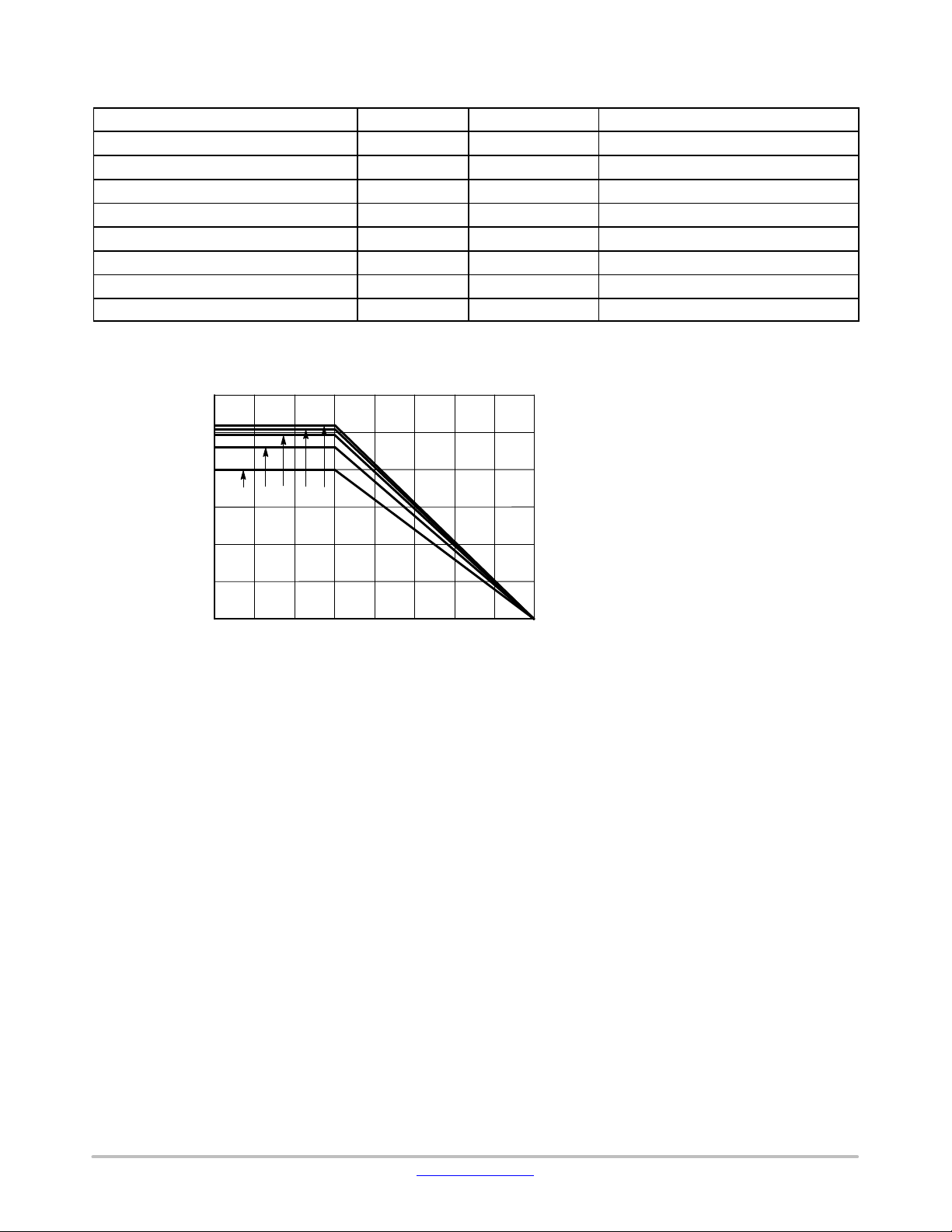
300
250
†
200
150
100
, POWER DISSIPATION (mW)
50
D
P
0
(1) (2) (3) (4) (5)
AMBIENT TEMPERATURE (°C)
150
1251007550250−25−50
Figure 1. Derating Curve
(1) SC−75 and SC−70/SOT−323; Minimum Pad
(2) SC−59; Minimum Pad
(3) SOT−23; Minimum Pad
(4) SOT−1123; 100 mm
(5) SOT−723; Minimum Pad
2
, 1 oz. copper trace
www.onsemi.com
2
Page 3
MUN2114, MMUN2114L, MUN5114, DTA114YE, DTA114YM3, NSBA114YF3
Table 2. THERMAL CHARACTERISTICS
Characteristic Symbol Max Unit
THERMAL CHARACTERISTICS (SC−59) (MUN2114)
Total Device Dissipation
= 25°C (Note 1)
T
A
Derate above 25°C (Note 1)
Thermal Resistance, (Note 1)
Junction to Ambient (Note 2)
Thermal Resistance, (Note 1)
Junction to Lead (Note 2)
Junction and Storage Temperature Range TJ, T
THERMAL CHARACTERISTICS (SOT−23) (MMUN2114L)
Total Device Dissipation
TA = 25°C (Note 1)
Derate above 25°C (Note 1)
Thermal Resistance, (Note 1)
Junction to Ambient (Note 2)
Thermal Resistance, (Note 1)
Junction to Lead (Note 2)
Junction and Storage Temperature Range TJ, T
THERMAL CHARACTERISTICS (SC−70/SOT−323) (MUN5114)
Total Device Dissipation
= 25°C (Note 1)
T
A
Derate above 25°C (Note 1)
Thermal Resistance, (Note 1)
Junction to Ambient (Note 2)
Thermal Resistance, (Note 1)
Junction to Lead (Note 2)
Junction and Storage Temperature Range TJ, T
THERMAL CHARACTERISTICS (SC−75) (DTA114YE)
Total Device Dissipation
= 25°C (Note 1)
T
A
Derate above 25°C (Note 1)
Thermal Resistance, (Note 1)
Junction to Ambient (Note 2)
Junction and Storage Temperature Range TJ, T
THERMAL CHARACTERISTICS (SOT−723) (DTA114YM3)
Total Device Dissipation
T
= 25°C (Note 1)
A
Derate above 25°C (Note 1)
Thermal Resistance, (Note 1)
Junction to Ambient (Note 2)
Junction and Storage Temperature Range TJ, T
1. FR−4 @ Minimum Pad.
2. FR−4 @ 1.0 x 1.0 Inch Pad.
3. FR−4 @ 100 mm
4. FR−4 @ 500 mm
2
, 1 oz. copper traces, still air.
2
, 1 oz. copper traces, still air.
(Note 2)
(Note 2)
(Note 2)
(Note 2)
(Note 2)
(Note 2)
(Note 2)
(Note 2)
(Note 2)
(Note 2)
P
D
230
mW
338
1.8
mW/°C
2.7
R
q
JA
R
q
JL
stg
P
D
540
370
264
287
−55 to +150 °C
246
°C/W
°C/W
mW
400
2.0
mW/°C
3.2
R
q
JA
R
q
JL
stg
P
D
508
311
174
208
−55 to +150 °C
202
°C/W
°C/W
mW
310
1.6
mW/°C
2.5
R
q
JA
R
q
JL
stg
P
D
618
403
280
332
−55 to +150 °C
200
°C/W
°C/W
mW
300
1.6
mW/°C
2.4
R
q
JA
stg
P
D
600
400
−55 to +150 °C
260
°C/W
mW
600
2.0
mW/°C
4.8
R
q
JA
stg
480
205
−55 to +150 °C
°C/W
www.onsemi.com
3
Page 4
MUN2114, MMUN2114L, MUN5114, DTA114YE, DTA114YM3, NSBA114YF3
Table 2. THERMAL CHARACTERISTICS
Characteristic UnitMaxSymbol
THERMAL CHARACTERISTICS (SOT−1123) (NSBA114YF3)
Total Device Dissipation
= 25°C (Note 3)
T
A
Derate above 25°C (Note 3)
Thermal Resistance, (Note 3)
Junction to Ambient (Note 4)
Thermal Resistance, Junction to Lead (Note 3)
Junction and Storage Temperature Range TJ, T
1. FR−4 @ Minimum Pad.
2. FR−4 @ 1.0 x 1.0 Inch Pad.
3. FR−4 @ 100 mm
4. FR−4 @ 500 mm
2
, 1 oz. copper traces, still air.
2
, 1 oz. copper traces, still air.
(Note 4)
(Note 4)
P
D
254
mW
297
2.0
mW/°C
2.4
R
q
JA
R
q
JL
stg
493
421
193 °C/W
−55 to +150 °C
°C/W
Table 3. ELECTRICAL CHARACTERISTICS (T
= 25°C, unless otherwise noted)
A
Characteristic Symbol Min Typ Max Unit
OFF CHARACTERISTICS
Collector−Base Cutoff Current
(VCB = 50 V, IE = 0)
Collector−Emitter Cutoff Current
(V
= 50 V, IB = 0)
CE
Emitter−Base Cutoff Current
(VEB = 6.0 V, IC = 0)
Collector−Base Breakdown Voltage
= 10 mA, IE = 0)
(I
C
Collector−Emitter Breakdown Voltage (Note 5)
(I
= 2.0 mA, IB = 0)
C
I
CBO
I
CEO
I
EBO
V
(BR)CBO
V
(BR)CEO
− − 100
− − 500
− − 0.2
50 − −
50 − −
nAdc
nAdc
mAdc
Vdc
Vdc
ON CHARACTERISTICS
DC Current Gain (Note 5)
= 5.0 mA, VCE = 10 V)
(I
C
Collector *Emitter Saturation Voltage (Note 5)
(IC = 10 mA, IB = 0.3 mA)
Input Voltage (off)
= 5.0 V, IC = 100 mA)
(V
CE
Input Voltage (on)
(V
= 0.2 V, IC = 1.0 mA)
CE
Output Voltage (on)
= 5.0 V, VB = 2.5 V, RL = 1.0 kW)
(V
CC
Output Voltage (off)
= 5.0 V, VB = 0.5 V, RL = 1.0 kW)
(V
CC
Input Resistor R1 7.0 10 13
Resistor Ratio R1/R
h
V
CE(sat)
V
V
V
V
FE
i(off)
i(on)
OL
OH
80 140 −
Vdc
− − 0.25
Vdc
− 0.7 0.5
Vdc
1.4 0.9 −
Vdc
− − 0.2
Vdc
4.9 − −
kW
2
0.17 0.21 0.25
5. Pulsed Condition: Pulse Width = 300 msec, Duty Cycle v 2%.
Product parametric performance is indicated in the Electrical Characteristics for the listed test conditions, unless otherwise noted. Product
performance may not be indicated by the Electrical Characteristics if operated under different conditions.
www.onsemi.com
4
Page 5
MUN2114, MMUN2114L, MUN5114, DTA114YE, DTA114YM3, NSBA114YF3
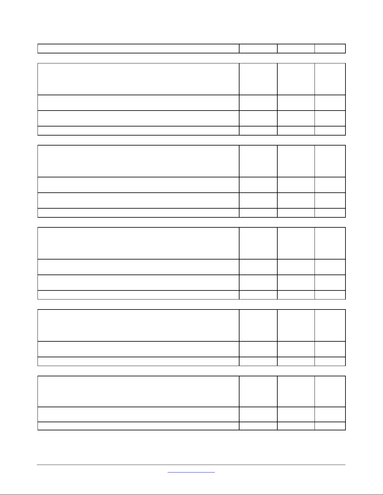
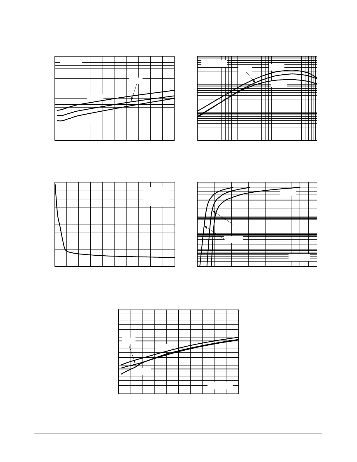
TYPICAL CHARACTERISTICS
MUN2114, MMUN2114L, MUN5114, DTA114YE, DTA114YM3
1
IC/IB = 10
25°C
0.1
150°C
−55°C
, COLLECTOR−EMITTER VOLTAGE (V)
0.01
01020
CE(sat)
V
I
, COLLECTOR CURRENT (mA)
C
Figure 2. V
CE(sat)
vs. I
4030
C
10
9
8
7
f = 10 kHz
= 0 A
I
E
T
= 25°C
A
6
5
4
3
2
, OUTPUT CAPACITANCE (pF)
1
ob
C
0
010 20304050
VR, REVERSE VOLTAGE (V)
Figure 4. Output Capacitance
1000
VCE = 10 V
100
10
, DC CURRENT GAIN
FE
h
1
50
0.1 1
100
10
1
0.1
0.01
, COLLECTOR CURRENT (mA)
C
I
0.001
01234
Figure 5. Output Current vs. Input Voltage
25°C
150°C
−55°C
I
, COLLECTOR CURRENT (mA)
C
Figure 3. DC Current Gain
25°C
150°C
V
, INPUT VOLTAGE (V)
in
10010
−55°C
VO = 5 V
56 7
100
10
1
, INPUT VOLTAGE (V)
in
V
0.1
25°C
−55°C
150°C
VO = 0.2 V
1002030
I
, COLLECTOR CURRENT (mA)
C
40 50
Figure 6. Input Voltage vs. Output Current
www.onsemi.com
5
Page 6

MUN2114, MMUN2114L, MUN5114, DTA114YE, DTA114YM3, NSBA114YF3
TYPICAL CHARACTERISTICS
NSBA114YF3
1
IC/IB = 10
0.1
150°C
−55°C
, COLLECTOR−EMITTER VOLTAGE (V)
0.01
01020
CE(sat)
V
I
, COLLECTOR CURRENT (mA)
C
Figure 7. V
7
6
5
4
25°C
CE(sat)
vs. I
C
4030
f = 10 kHz
= 0 A
I
E
T
= 25°C
A
1000
VCE = 10 V
100
10
, DC CURRENT GAIN
FE
h
1
50
0.1 1
100
10
1
25°C
150°C
−55°C
I
, COLLECTOR CURRENT (mA)
C
Figure 8. DC Current Gain
−55°C
10010
3
2
, OUTPUT CAPACITANCE (pF)
1
ob
C
0
010 20304050
VR, REVERSE VOLTAGE (V)
Figure 9. Output Capacitance
100
10
25°C
1
, INPUT VOLTAGE (V)
in
V
150°C
0.1
1002030
I
, COLLECTOR CURRENT (mA)
C
Figure 11. Input Voltage vs. Output Current
−55°C
0.1
0.01
, COLLECTOR CURRENT (mA)
C
I
0.001
01 2 3 4
Figure 10. Output Current vs. Input Voltage
VO = 0.2 V
40 50
25°C
150°C
567
V
, INPUT VOLTAGE (V)
in
VO = 5 V
11101112
www.onsemi.com
6
Page 7

MECHANICAL CASE OUTLINE
PACKAGE DIMENSIONS
SCALE 4:1
D
3
E
1
2
e
TOP VIEW
A
A1
SIDE VIEW
RECOMMENDED
SOLDERING FOOTPRINT
2.90
3X
H
E
b
SEE VIEW C
END VIEW
3X
0.90
SOT−23 (TO−236)
CASE 318−08
ISSUE AS
0.25
T
L
L1
VIEW C
c
DATE 30 JAN 2018
NOTES:
1. DIMENSIONING AND TOLERANCING PER ASME Y14.5M, 1994.
2. CONTROLLING DIMENSION: MILLIMETERS.
3. MAXIMUM LEAD THICKNESS INCLUDES LEAD FINISH.
MINIMUM LEAD THICKNESS IS THE MINIMUM THICKNESS OF
THE BASE MATERIAL.
4. DIMENSIONS D AND E DO NOT INCLUDE MOLD FLASH,
PROTRUSIONS, OR GATE BURRS.
DIMAMIN NOM MAX MIN
A1 0.01 0.06 0.10 0.000
b 0.37 0.44 0.50 0.015
c 0.08 0.14 0.20 0.003
D 2.80 2.90 3.04 0.110
E 1.20 1.30 1.40 0.047
e 1.78 1.90 2.04 0.070
L 0.30 0.43 0.55 0.012
L1
H
E
MILLIMETERS
0.89 1.00 1.11 0.035
0.35 0.54 0.69 0.014 0.021 0.027
2.10 2.40 2.64 0.083 0.094 0.104
0 −−− 10 0 −−− 10T°°°°
INCHES
NOM MAX
0.039 0.044
0.002 0.004
0.017 0.020
0.006 0.008
0.114 0.120
0.051 0.055
0.075 0.080
0.017 0.022
GENERIC
MARKING DIAGRAM*
XXXMG
G
1
XXX = Specific Device Code
M = Date Code
G = Pb−Free Package
3X
0.80
0.95
PITCH
DIMENSIONS: MILLIMETERS
STYLE 1 THRU 5:
CANCELLED
STYLE 9:
PIN 1. ANODE
2. ANODE
3. CATHODE
STYLE 15:
PIN 1. GATE
2. CATHODE
3. ANODE
STYLE 21:
PIN 1. GATE
2. SOURCE
3. DRAIN
STYLE 27:
PIN 1. CATHODE
2. CATHODE
3. CATHODE
DOCUMENT NUMBER:
DESCRIPTION:
ON Semiconductor and are trademarks of Semiconductor Components Industries, LLC dba ON Semiconductor or its subsidiaries in the United States and/or other countries.
ON Semiconductor reserves the right to make changes without further notice to any products herein. ON Semiconductor makes no warranty, representation or guarantee regarding
the suitability of its products for any particular purpose, nor does ON Semiconductor assume any liability arising out of the application or use of any product or circuit, and specifically
disclaims any and all liability, including without limitation special, consequential or incidental damages. ON Semiconductor does not convey any license under its patent rights nor the
rights of others.
STYLE 6:
PIN 1. BASE
2. EMITTER
3. COLLECTOR
STYLE 10:
PIN 1. DRAIN
2. SOURCE
3. GATE
STYLE 16:
PIN 1. ANODE
2. CATHODE
3. CATHODE
STYLE 22:
PIN 1. RETURN
2. OUTPUT
3. INPUT
STYLE 28:
PIN 1. ANODE
2. ANODE
3. ANODE
98ASB42226B
SOT−23 (TO−236)
STYLE 7:
PIN 1. EMITTER
2. BASE
3. COLLECTOR
STYLE 11:
PIN 1. ANODE
2. CATHODE
3. CATHODE−ANODE
STYLE 17:
PIN 1. NO CONNECTION
2. ANODE
3. CATHODE
STYLE 23:
PIN 1. ANODE
2. ANODE
3. CATHODE
STYLE 8:
PIN 1. ANODE
2. NO CONNECTION
3. CATHODE
STYLE 12:
PIN 1. CATHODE
2. CATHODE
3. ANODE
STYLE 18:
PIN 1. NO CONNECTION
2. CATHODE
3. ANODE
STYLE 24:
PIN 1. GATE
2. DRAIN
3. SOURCE
Electronic versions are uncontrolled except when accessed directly from the Document Repository.
Printed versions are uncontrolled except when stamped “CONTROLLED COPY” in red.
*This information is generic. Please refer to
device data sheet for actual part marking.
Pb−Free indicator, “G” or microdot “ G”,
may or may not be present.
STYLE 13:
PIN 1. SOURCE
2. DRAIN
3. GATE
STYLE 19:
PIN 1. CATHODE
2. ANODE
3. CATHODE−ANODE
STYLE 25:
PIN 1. ANODE
2. CATHODE
3. GATE
STYLE 14:
PIN 1. CATHODE
2. GATE
3. ANODE
STYLE 20:
PIN 1. CATHODE
2. ANODE
3. GATE
STYLE 26:
PIN 1. CATHODE
2. ANODE
3. NO CONNECTION
PAGE 1 OF 1
© Semiconductor Components Industries, LLC, 2019
www.onsemi.com
Page 8

MECHANICAL CASE OUTLINE
PACKAGE DIMENSIONS
SCALE 2:1
SC−59
CASE 318D−04
ISSUE H
DATE 28 JUN 2012
D
H
E
3
1
E
2
b
e
C
A1
A
L
SOLDERING FOOTPRINT*
0.95
0.95
0.037
1.0
0.039
0.8
0.031
*For additional information on our Pb−Free strategy and soldering
details, please download the ON Semiconductor Soldering and
Mounting Techniques Reference Manual, SOLDERRM/D.
0.037
0.094
SCALE 10:1
2.4
ǒ
inches
mm
Ǔ
NOTES:
1. DIMENSIONING AND TOLERANCING PER ANSI Y14.5M, 1982.
2. CONTROLLING DIMENSION: MILLIMETER.
DIMAMIN NOM MAX MIN
A1 0.01 0.06 0.10 0.001
b 0.35 0.43 0.50 0.014
c 0.09 0.14 0.18 0.003
D 2.70 2.90 3.10 0.106
E 1.30 1.50 1.70 0.051
e 1.70 1.90 2.10 0.067
L 0.20 0.40 0.60 0.008
H
E
MILLIMETERS
1.00 1.15 1.30 0.039
2.50 2.80 3.00 0.099
GENERIC
MARKING DIAGRAM
XXX MG
G
1
XXX = Specific Device Code
M = Date Code
G = Pb−Free Package*
(*Note: Microdot may be in either location)
*This information is generic. Please refer to
device data sheet for actual part marking.
Pb−Free indicator, “G” or microdot “ G”,
may or may not be present.
STYLE 1:
PIN 1. BASE
2. EMITTER
3. COLLECTOR
STYLE 4:
PIN 1. CATHODE
2. N.C.
3. ANODE
STYLE 2:
PIN 1. ANODE
2. N.C.
3. CATHODE
STYLE 5:
PIN 1. CATHODE
2. CATHODE
3. ANODE
INCHES
NOM MAX
0.045 0.051
0.002 0.004
0.017 0.020
0.005 0.007
0.114 0.122
0.059 0.067
0.075 0.083
0.016 0.024
0.110 0.118
STYLE 3:
PIN 1. ANODE
2. ANODE
3. CATHODE
STYLE 6:
PIN 1. ANODE
2. CATHODE
3. ANODE/CATHODE
DOCUMENT NUMBER:
DESCRIPTION:
ON Semiconductor and are trademarks of Semiconductor Components Industries, LLC dba ON Semiconductor or its subsidiaries in the United States and/or other countries.
ON Semiconductor reserves the right to make changes without further notice to any products herein. ON Semiconductor makes no warranty, representation or guarantee regarding
the suitability of its products for any particular purpose, nor does ON Semiconductor assume any liability arising out of the application or use of any product or circuit, and specifically
disclaims any and all liability, including without limitation special, consequential or incidental damages. ON Semiconductor does not convey any license under its patent rights nor the
rights of others.
© Semiconductor Components Industries, LLC, 2019
98ASB42664B
SC−59
Electronic versions are uncontrolled except when accessed directly from the Document Repository.
Printed versions are uncontrolled except when stamped “CONTROLLED COPY” in red.
PAGE 1 OF 1
www.onsemi.com
Page 9

MECHANICAL CASE OUTLINE
PACKAGE DIMENSIONS
SCALE 4:1
D
e1
3
E
b
A
0.05 (0.002)
H
E
12
e
A1
SC−70 (SOT−323)
CASE 419−04
ISSUE N
A2
DATE 11 NOV 2008
NOTES:
1. DIMENSIONING AND TOLERANCING PER ANSI Y14.5M, 1982.
2. CONTROLLING DIMENSION: INCH.
DIMAMIN NOM MAX MIN
A1 0.00 0.05 0.10 0.000
A2 0.70 REF
b 0.30 0.35 0.40 0.012
c 0.10 0.18 0.25 0.004
D 1.80 2.10 2.20 0.071
E 1.15 1.24 1.35 0.045
e 1.20 1.30 1.40 0.047
e1
L
H
E
MILLIMETERS
0.80 0.90 1.00 0.032
0.65 BSC
0.38
0.20 0.56
2.00 2.10 2.40 0.079 0.083 0.095
INCHES
NOM MAX
0.035 0.040
0.002 0.004
0.028 REF
0.014 0.016
0.007 0.010
0.083 0.087
0.049 0.053
0.051 0.055
0.026 BSC
0.015
0.008 0.022
c
GENERIC
L
MARKING DIAGRAM
SOLDERING FOOTPRINT*
0.65
0.65
0.025
0.9
0.035
0.7
0.028
*For additional information on our Pb−Free strategy and soldering
details, please download the ON Semiconductor Soldering and
Mounting Techniques Reference Manual, SOLDERRM/D.
STYLE 1:
STYLE 6:
PIN 1. EMITTER
2. BASE
3. COLLECTOR
CANCELLED
STYLE 2:
PIN 1. ANODE
2. N.C.
3. CATHODE
STYLE 7:
PIN 1. BASE
2. EMITTER
3. COLLECTOR
0.025
1.9
0.075
SCALE 10:1
STYLE 3:
PIN 1. BASE
2. EMITTER
3. COLLECTOR
STYLE 8:
PIN 1. GATE
2. SOURCE
3. DRAIN
ǒ
inches
mm
Ǔ
STYLE 4:
STYLE 9:
PIN 1. CATHODE
2. CATHODE
3. ANODE
PIN 1. ANODE
2. CATHODE
3. CATHODE-ANODE
XX MG
G
1
XX = Specific Device Code
M = Date Code
G = Pb−Free Package
*This information is generic. Please refer to
device data sheet for actual part marking.
Pb−Free indicator, “G” or microdot “ G”,
may or may not be present.
STYLE 5:
PIN 1. ANODE
2. ANODE
3. CATHODE
STYLE 10:
PIN 1. CATHODE
2. ANODE
3. ANODE-CATHODE
STYLE 11:
PIN 1. CATHODE
2. CATHODE
3. CATHODE
DOCUMENT NUMBER:
DESCRIPTION:
ON Semiconductor and are trademarks of Semiconductor Components Industries, LLC dba ON Semiconductor or its subsidiaries in the United States and/or other countries.
ON Semiconductor reserves the right to make changes without further notice to any products herein. ON Semiconductor makes no warranty, representation or guarantee regarding
the suitability of its products for any particular purpose, nor does ON Semiconductor assume any liability arising out of the application or use of any product or circuit, and specifically
disclaims any and all liability, including without limitation special, consequential or incidental damages. ON Semiconductor does not convey any license under its patent rights nor the
rights of others.
© Semiconductor Components Industries, LLC, 2019
98ASB42819B
SC−70 (SOT−323)
Electronic versions are uncontrolled except when accessed directly from the Document Repository.
Printed versions are uncontrolled except when stamped “CONTROLLED COPY” in red.
PAGE 1 OF 1
www.onsemi.com
Page 10

MECHANICAL CASE OUTLINE
PACKAGE DIMENSIONS
3
1
SCALE 4:1
2
3 PL
b
0.20 (0.008) D
M
C
STYLE 1:
PIN 1. BASE
2. EMITTER
3. COLLECTOR
STYLE 4:
PIN 1. CATHODE
2. CATHODE
3. ANODE
−E−
2
3
1
L
STYLE 2:
PIN 1. ANODE
STYLE 5:
PIN 1. GATE
e
−D−
H
E
A1
2. N/C
3. CATHODE
2. SOURCE
3. DRAIN
SC−75/SOT−416
CASE 463−01
ISSUE G
0.20 (0.008) E
A
STYLE 3:
PIN 1. ANODE
2. ANODE
3. CATHODE
SOLDERING FOOTPRINT*
0.356
0.014
DATE 07 AUG 2015
NOTES:
1. DIMENSIONING AND TOLERANCING PER ANSI
Y14.5M, 1982.
2. CONTROLLING DIMENSION: MILLIMETER.
MILLIMETERS
DIM MIN NOM MAX
A 0.70 0.80 0.90
A1 0.00 0.05 0.10
b
0.15 0.20 0.30 0.006 0.008 0.012
C 0.10 0.15 0.25
D 1.55 1.60 1.65
E
0.70 0.80 0.90 0.027 0.031 0.035
e 1.00 BSC
L 0.10 0.15 0.20
H
1.50 1.60 1.70
E
INCHES
MIN NOM MAX
0.027 0.031 0.035
0.000 0.002 0.004
0.004 0.006 0.010
0.061 0.063 0.065
0.04 BSC
0.004 0.006 0.008
0.060 0.063 0.067
GENERIC
MARKING DIAGRAM*
XX M
G
1
XX = Specific Device Code
M = Date Code
G = Pb−Free Package
*This information is generic. Please refer to
device data sheet for actual part marking.
Pb−Free indicator, “G” or microdot “ G”,
may or may not be present.
1.803
0.071
0.508
0.020
0.787
0.031
1.000
0.039
SCALE 10:1
ǒ
inches
mm
Ǔ
*For additional information on our Pb−Free strategy and soldering
details, please download the ON Semiconductor Soldering and
Mounting Techniques Reference Manual, SOLDERRM/D.
DOCUMENT NUMBER:
DESCRIPTION:
ON Semiconductor and are trademarks of Semiconductor Components Industries, LLC dba ON Semiconductor or its subsidiaries in the United States and/or other countries.
ON Semiconductor reserves the right to make changes without further notice to any products herein. ON Semiconductor makes no warranty, representation or guarantee regarding
the suitability of its products for any particular purpose, nor does ON Semiconductor assume any liability arising out of the application or use of any product or circuit, and specifically
disclaims any and all liability, including without limitation special, consequential or incidental damages. ON Semiconductor does not convey any license under its patent rights nor the
rights of others.
© Semiconductor Components Industries, LLC, 2019
98ASB15184C
SC−75/SOT−416
Electronic versions are uncontrolled except when accessed directly from the Document Repository.
Printed versions are uncontrolled except when stamped “CONTROLLED COPY” in red.
PAGE 1 OF 1
www.onsemi.com
Page 11

MECHANICAL CASE OUTLINE
PACKAGE DIMENSIONS
SCALE 8:1
1
2
TOP VIEW
c
SIDE VIEW
3X
L2
e
2X
b1
BOTTOM VIEW
SOLDERING FOOTPRINT*
1.20
3X
0.34
1
−X−
D
−Y−
3
E
A
H
E
b
3X
L
0.26
CASE 524AA
0.08 XY
SOT−1123
ISSUE C
NOTES:
1. DIMENSIONING AND TOLERANCING PER ASME
Y14.5M, 1994.
2. CONTROLLING DIMENSION: MILLIMETERS.
3. MAXIMUM LEAD THICKNESS INCLUDES LEAD
FINISH. MINIMUM LEAD THICKNESS IS THE
MINIMUM THICKNESS OF BASE MATERIAL.
4. DIMENSIONS D AND E DO NOT INCLUDE MOLD
FLASH, PROTRUSIONS, OR GATE BURRS.
MILLIMETERS
DIM MIN MAX
A 0.34 0.40
b 0.15 0.28
b1 0.10 0.20
c 0.07 0.17
D 0.75 0.85
E 0.55 0.65
e
0.35 0.40
H
0.95 1.05
E
L 0.185 REF
L2 0.05 0.15
GENERIC
MARKING DIAGRAM*
X M
X = Specific Device Code
M = Date Code
*This information is generic. Please refer
to device data sheet for actual part
marking.
Pb−Free indicator, “G” or microdot “ G”,
may or may not be present.
DATE 29 NOV 2011
0.38
2X
0.20
PACKAGE
OUTLINE
DIMENSIONS: MILLIMETERS
*For additional information on our Pb−Free strategy and soldering
details, please download the ON Semiconductor Soldering and
Mounting Techniques Reference Manual, SOLDERRM/D.
STYLE 1:
PIN 1. BASE
2. EMITTER
3. COLLECTOR
DOCUMENT NUMBER:
DESCRIPTION:
ON Semiconductor and are trademarks of Semiconductor Components Industries, LLC dba ON Semiconductor or its subsidiaries in the United States and/or other countries.
ON Semiconductor reserves the right to make changes without further notice to any products herein. ON Semiconductor makes no warranty, representation or guarantee regarding
the suitability of its products for any particular purpose, nor does ON Semiconductor assume any liability arising out of the application or use of any product or circuit, and specifically
disclaims any and all liability, including without limitation special, consequential or incidental damages. ON Semiconductor does not convey any license under its patent rights nor the
rights of others.
STYLE 2:
PIN 1. ANODE
2. N/C
3. CATHODE
STYLE 3:
PIN 1. ANODE
2. ANODE
3. CATHODE
98AON23134D
STYLE 4:
PIN 1. CATHODE
2. CATHODE
3. ANODE
Electronic versions are uncontrolled except when accessed directly from the Document Repository.
Printed versions are uncontrolled except when stamped “CONTROLLED COPY” in red.
STYLE 5:
PIN 1. GATE
2. SOURCE
3. DRAIN
SOT−1123, 3−LEAD, 1.0X0.6X0.37, 0.35P
PAGE 1 OF 1
© Semiconductor Components Industries, LLC, 2019
www.onsemi.com
Page 12

MECHANICAL CASE OUTLINE
PACKAGE DIMENSIONS
SCALE 4:1
−X−
D
2X
b1
3
1
e
TOP VIEW
1
−Y−
E
2
b
2X
X0.08 Y
3X
L
SOT−723
CASE 631AA−01
ISSUE D
A
H
E
C
SIDE VIEW
DATE 10 AUG 2009
NOTES:
1. DIMENSIONING AND TOLERANCING PER ASME
Y14.5M, 1994.
2. CONTROLLING DIMENSION: MILLIMETERS.
3. MAXIMUM LEAD THICKNESS INCLUDES LEAD
FINISH. MINIMUM LEAD THICKNESS IS THE MINIMUM
THICKNESS OF BASE MATERIAL.
4. DIMENSIONS D AND E DO NOT INCLUDE MOLD
FLASH, PROTRUSIONS OR GATE BURRS.
MILLIMETERS
DIM MIN NOM MAX
A 0.45 0.50 0.55
b 0.15 0.21 0.27
b1 0.25 0.31 0.37
C 0.07 0.12 0.17
D 1.15 1.20 1.25
E 0.75 0.80 0.85
e
H 1.15 1.20 1.25
L
L2 0.15 0.20 0.25
0.40 BSC
E
0.29 REF
3X
L2
BOTTOM VIEW
STYLE 1:
PIN 1. BASE
2. EMITTER
3. COLLECTOR
STYLE 2:
PIN 1. ANODE
2. N/C
3. CATHODE
STYLE 3:
PIN 1. ANODE
2. ANODE
3. CATHODE
STYLE 4:
RECOMMENDED
SOLDERING FOOTPRINT*
2X
0.40
2X
0.27
PACKAGE
OUTLINE
1.50
3X
0.52
*For additional information on our Pb−Free strategy and soldering
details, please download the ON Semiconductor Soldering and
Mounting Techniques Reference Manual, SOLDERRM/D.
0.36
DIMENSIONS: MILLIMETERS
PIN 1. CATHODE
2. CATHODE
3. ANODE
STYLE 5:
PIN 1. GATE
2. SOURCE
3. DRAIN
GENERIC
MARKING DIAGRAM*
XX M
1
XX = Specific Device Code
M = Date Code
*This information is generic. Please refer
to device data sheet for actual part
marking. Pb−Free indicator, “G”, may
or not be present.
DOCUMENT NUMBER:
DESCRIPTION:
ON Semiconductor and are trademarks of Semiconductor Components Industries, LLC dba ON Semiconductor or its subsidiaries in the United States and/or other countries.
ON Semiconductor reserves the right to make changes without further notice to any products herein. ON Semiconductor makes no warranty, representation or guarantee regarding
the suitability of its products for any particular purpose, nor does ON Semiconductor assume any liability arising out of the application or use of any product or circuit, and specifically
disclaims any and all liability, including without limitation special, consequential or incidental damages. ON Semiconductor does not convey any license under its patent rights nor the
rights of others.
© Semiconductor Components Industries, LLC, 2019
98AON12989D
SOT−723
Electronic versions are uncontrolled except when accessed directly from the Document Repository.
Printed versions are uncontrolled except when stamped “CONTROLLED COPY” in red.
PAGE 1 OF 1
www.onsemi.com
Page 13

ON Semiconductor and are trademarks of Semiconductor Components Industries, LLC dba ON Semiconductor or its subsidiaries in the United States and/or other countries.
ON Semiconductor owns the rights to a number of patents, trademarks, copyrights, trade secrets, and other intellectual property. A listing of ON Semiconductor’s product/patent
coverage may be accessed at www.onsemi.com/site/pdf/Patent−Marking.pdf
ON Semiconductor makes no warranty, representation or guarantee regarding the suitability of its products for any particular purpose, nor does ON Semiconductor assume any liability
arising out of the application or use of any product or circuit, and specifically disclaims any and all liability, including without limitation special, consequential or incidental damages.
Buyer is responsible for its products and applications using ON Semiconductor products, including compliance with all laws, regulations and safety requirements or standards,
regardless of any support or applications information provided by ON Semiconductor. “Typical” parameters which may be provided in ON Semiconductor data sheets and/or
specifications can and do vary in different applications and actual performance may vary over time. All operating parameters, including “Typicals” must be validated for each customer
application by customer’s technical experts. ON Semiconductor does not convey any license under its patent rights nor the rights of others. ON Semiconductor products are not
designed, intended, or authorized for use as a critical component in life support systems or any FDA Class 3 medical devices or medical devices with a same or similar classification
in a foreign jurisdiction or any devices intended for implantation in the human body. Should Buyer purchase or use ON Semiconductor products for any such unintended or unauthorized
application, Buyer shall indemnify and hold ON Semiconductor and its officers, employees, subsidiaries, affiliates, and distributors harmless against all claims, costs, damages, and
expenses, and reasonable attorney fees arising out of, directly or indirectly, any claim of personal injury or death associated with such unintended or unauthorized use, even if such
claim alleges that ON Semiconductor was negligent regarding the design or manufacture of the part. ON Semiconductor is an Equal Opportunity/Affirmative Action Employer. This
literature is subject to all applicable copyright laws and is not for resale in any manner.
. ON Semiconductor reserves the right to make changes without further notice to any products herein.
PUBLICATION ORDERING INFORMATION
LITERATURE FULFILLMENT:
Email Requests to: orderlit@onsemi.com
ON Semiconductor Website: www.onsemi.com
TECHNICAL SUPPORT
North American Technical Support:
Voice Mail: 1 800−282−9855 Toll Free USA/Canada
Phone: 011 421 33 790 2910
Europe, Middle East and Africa Technical Support:
Phone: 00421 33 790 2910
For additional information, please contact your local Sales Representative
◊
www.onsemi.com
1
Page 14

Mouser Electronics
Authorized Distributor
Click to View Pricing, Inventory, Delivery & Lifecycle Information:
ON Semiconductor:
MUN2114T1 MUN5114T1 MUN5114T1G MMUN2114LT1 MMUN2114LT1G DTA114YE DTA114YET1
DTA114YET1G DTA114YM3T5G MUN2114T1G SMUN2114T1G SDTA114YET1G MMUN2114LT3G
NSBA114YF3T5G SMMUN2114LT1G SMUN5114T3G SMUN5114T1G NSVDTA114YM3T5G NSVMMUN2114LT3G
 Loading...