

Datasheet DTA144ERLRP, DTA144ERLRM, DTA144ERLRA, DTB113ERLRP, DTB113ERLRM Datasheet (ON Semiconductor)
...Page 1
Semiconductor Components Industries, LLC, 2000
May, 2000 – Rev. 0
1 Publication Order Number:
DTA114E/D
DTA114E SERIES
Preferred Devices
Bias Resistor Transistor
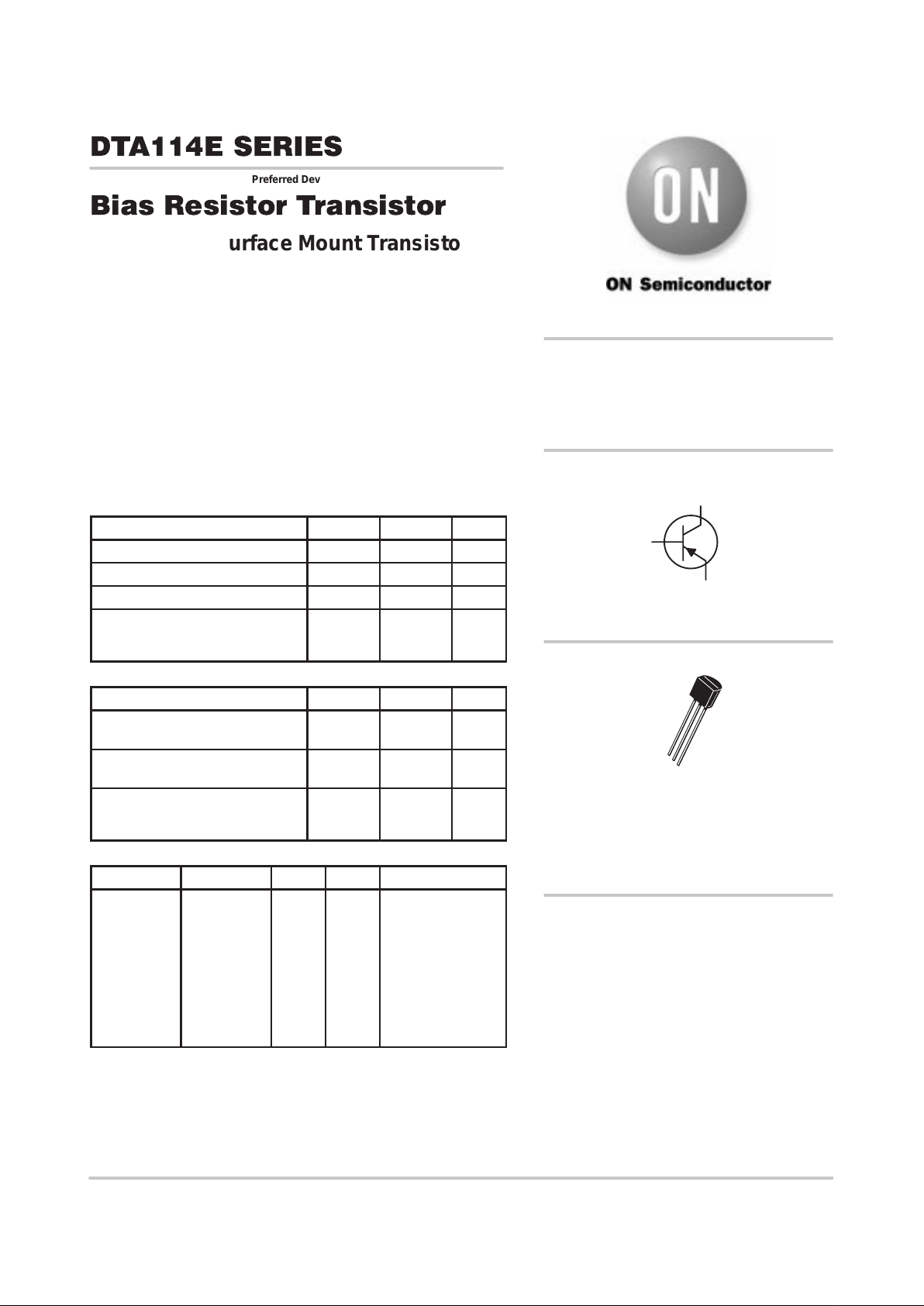
PNP Silicon Surface Mount Transistor
with Monolithic Bias Resistor Network
This new series of digital transistors is designed to replace a single
device and its external resistor bias network. The BRT (Bias Resistor
Transistor) contains a single transistor with a monolithic bias network
consisting of two resistors; a series base resistor and a base–emitter
resistor. The BRT eliminates these individual components by
integrating them into a single device. The use of a BRT can reduce
both system cost and board space. The device is housed in the TO–92
package which is designed for through hole applications.
MAXIMUM RATINGS (T
A
= 25°C unless otherwise noted)
Rating Symbol Value Unit
Collector-Base Voltage V
CBO
50 Vdc
Collector-Emitter Voltage V
CEO
50 Vdc
Collector Current I
C
100 mAdc
Total Power Dissipation
@ T
A
= 25°C
(1.)
Derate above 25°C
P
D
350
2.81
mW
mW/°C
THERMAL CHARACTERISTICS
Characteristic Symbol Value Unit
Thermal Resistance, Junction to
Ambient (surface mounted)
R
θ
JA
357 °C/W
Operating and Storage
T emperature Range
TJ, T
stg
–55 to
+150
°C
Maximum Temperature for
Soldering Purposes,
Time in Solder Bath
T
L
260
10
°C
Sec
DEVICE MARKING AND RESISTOR VALUES
Device Marking R1 (K) R2 (K) Shipping
DTA114E
DTA124E
DTA144E
DTA114Y
DTA114T
DTA143T
DTB113E
DTA123E
DTA143E
DTA143Z
DTA114E
DTA124E
DTA144E
DTA114Y
DTA114T
DTA143T
DTB113E
DTA123E
DTA143E
DTA143Z
10
22
47
10
10
4.7
1.0
2.2
4.7
4.7
10
22
47
47
∞
∞
1.0
2.2
4.7
47
5000/Box
1. Device mounted on a FR–4 glass epoxy printed circuit board using the
minimum recommended footprint.
http://onsemi.com
CASE 29
TO–92 (TO–226)
STYLE 1
Preferred devices are recommended choices for future use
and best overall value.
PNP SILICON
BIAS RESISTOR
TRANSISTOR
1
2
3
COLLECTOR
3
2
BASE
1
EMITTER
Page 2
DTA114E SERIES
http://onsemi.com
2
ELECTRICAL CHARACTERISTICS (T
A
= 25°C unless otherwise noted)
Characteristic
Symbol Min Typ Max Unit
OFF CHARACTERISTICS
Collector–Base Cutoff Current (VCB = 50 V, IE = 0) I
CBO
— — 100 nAdc
Collector–Emitter Cutoff Current (VCE = 50 V, IB = 0) I
CEO
— — 500 nAdc
Emitter–Base Cutoff Current DTA114E
(V
EB
= 6.0 V, IC = 0) DTA124E
DTA144E
DTA114Y
DTA114T
DTA143T
DTB113E
DTA123E
DTA143E
DTA143Z
I
EBO
—
—
—
—
—
—
—
—
—
—
—
—
—
—
—
—
—
—
—
—
0.5
0.2
0.1
0.2
0.9
1.9
4.3
2.3
1.5
0.18
mAdc
Collector–Base Breakdown Voltage (IC = 10 µA, IE = 0) V
(BR)CBO
50 — — Vdc
Collector–Emitter Breakdown Voltage
(2.)
(IC = 2.0 mA, IB = 0) V
(BR)CEO
50 — — Vdc
ON CHARACTERISTICS
(2.)
DC Current Gain DTA114E
(V
CE
= 10 V, IC = 5.0 mA) DTA124E
DTA144E
DTA114Y
DTA114T
DTA143T
DTB113E
DTA123E
DTA143E
DTA143Z
h
FE
35
60
80
80
160
160
3.0
8.0
15
80
60
100
140
140
250
250
5.0
15
27
140
—
—
—
—
—
—
—
—
—
—
Collector–Emitter Saturation Voltage
(I
C
= 10 mA, IE = 0.3 mA) DTA144E/DTA114Y
(I
C
= 10 mA, IE = 0.3 mA) DTB113E/DTA143E
(I
C
= 10 mA, IB = 5 mA) DTA123E
(I
C
= 10 mA, IB = 1 mA) DTA114T/DTA143T/
(I
C
= 10 mA, IB = 1 mA) DTA143Z/DTA124E
V
CE(sat)
— — 0.25 Vdc
Output Voltage (on)
(V
CC
= 5.0 V, VB = 2.5 V, RL = 1.0 kΩ) DTA114E
DTA124E
DTA114Y
DTA114T
DTA143T
DTB113E
DTA123E
DTA143E
DTA143Z
(V
CC
= 5.0 V, VB = 3.5 V, RL = 1.0 kΩ) DTA144E
V
OL
—
—
—
—
—
—
—
—
—
—
—
—
—
—
—
—
—
—
—
—
0.2
0.2
0.2
0.2
0.2
0.2
0.2
0.2
0.2
0.2
Vdc
2. Pulse Test: Pulse Width < 300 µs, Duty Cycle < 2.0%
Page 3

DTA114E SERIES
http://onsemi.com
3
ELECTRICAL CHARACTERISTICS (T
A
= 25°C unless otherwise noted) (Continued)
Characteristic
Symbol Min Typ Max Unit
Output Voltage (of f)
(V
CC
= 5.0 V, VB = 0.5 V, RL = 1.0 kΩ) DTA114T
DTA113T
DTA144E
DTA114Y
DTA143Z
(V
CC
= 5.0 V, VB = 0.05 V, RL = 1.0 kΩ) DTB113E
(V
CC
= 5.0 V, VB = 0.25 V, RL = 1.0 kΩ) DTA114T
DTA143T
DTA123E
DTA143E
V
OH
4.9 — — Vdc
Input Resistor DTA114E
DTA124E
DTA144E
DTA114Y
DTA114T
DTA143T
DTB113E
DTA123E
DTA143E
DTA143Z
R1 7.0
15.4
32.9
7.0
7.0
3.3
0.7
1.5
3.3
3.3
10
22
47
10
10
4.7
1.0
2.2
4.7
4.7
13
28.6
61.1
13
13
6.1
1.3
2.9
6.1
6.1
kΩ
Resistor Ratio DTA114E/DTA124E/DTA144E
DTA114Y
DTA114T/DTA143T
DTB113E/DTA123E/DT A143E
DTA143Z
R1/R
2
0.8
0.17
—
0.8
0.055
1.0
0.21
—
1.0
0.1
1.2
0.25
—
1.2
0.185
Page 4

DTA114E SERIES
http://onsemi.com
4
TYPICAL ELECTRICAL CHARACTERISTICS
DT A114E
100
10
1
0.1
0.01
0.001
0
V
in
, INPUT VOLTAGE (VOLTS)
I
C
, COLLECTOR CURRENT (mA)
TA= –25°C
25°C
12345
678910
0.01
20
I
C
, COLLECTOR CURRENT (mA)
V
CE(sat)
, MAXIMUM COLLECTOR VOLTAGE (VOLTS)
0.1
1
0406080
1000
1 10 100
I
C
, COLLECTOR CURRENT (mA)
h
FE
, DC CURRENT GAIN (NORMALIZED)
TA=75°C
–25°C
100
10
75°C
50
010 20 3040
4
3
1
2
V
R
, REVERSE BIAS VOLTAGE (VOLTS)
C
ob
, CAPACITANCE (pF)
0
TA= –25°C
25°C
75°C
f = 1 MHz
l
E
= 0 V
T
A
= 25°C
VO = 5 V
IC/IB=10
VCE = 10 V
0
I
C
, COLLECTOR CURRENT (mA)
0.1
V
in
, INPUT VOLTAGE (VOLTS)
1
10
100
10 20 30 40 50
TA= –25°C
25°C
75°C
VO = 0.2 V
Figure 1. Derating Curve
250
200
150
100
50
0
–50 0 50 100 150
T
A
, AMBIENT TEMPERATURE (°C)
P
D
, POWER DISSIPATION (MILLIWATTS)
R
θ
JA
= 625°C/W
Figure 2. V
CE(sat)
versus I
C
Figure 3. DC Current Gain
Figure 4. Output Capacitance
Figure 5. Output Current versus Input Voltage
Figure 6. Input Voltage versus Output Current
25°C
Page 5

DTA114E SERIES
http://onsemi.com
5
TYPICAL ELECTRICAL CHARACTERISTICS
DT A124E
Figure 7. V
CE(sat)
versus I
C
Figure 8. DC Current Gain
1000
10
IC, COLLECTOR CURRENT (mA)
h
FE
, DC CURRENT GAIN (NORMALIZED)
100
10
1
100
TA=75°C
25°C
–25°C
Figure 9. Output Capacitance
IC, COLLECTOR CURRENT (mA)
0
10 20 30
TA= –25°C
75°C
V
in
, INPUT VOLTAGE (VOLTS)
100
10
1
0.1
40 50
Figure 10. Output Current versus Input Voltage
100
10
1
0.1
0.01
0.001
01 2 3 4
V
in
, INPUT VOLTAGE (VOLTS)
75°C
25°C
TA= –25°C
I
C
, COLLECTOR CURRENT (mA)
5678910
Figure 11. Input Voltage versus Output Current
0.01
V
CE(sat)
,
MA
X
IM
U
M
COLLECTOR
VOLTA
G
E
(
VOLTS)
0.1
1
10
40
IC, COLLECTOR CURRENT (mA)
020 6080
75°C
25°C
TA= –25°C
50
010 2030 40
4
3
2
1
0
V
R
, REVERSE BIAS VOLTAGE (VOLTS)
C
ob
,
CA
P
ACITA
N
CE
(p
F)
25°C
f = 1 MHz
l
E
= 0 V
T
A
= 25°C
VO = 5 V
VO = 0.2 V
IC/IB=10
VCE = 10 V
Page 6

DTA114E SERIES
http://onsemi.com
6
TYPICAL ELECTRICAL CHARACTERISTICS
DT A144E
Figure 12. V
CE(sat)
versus I
C
100
10
1
0.1
010203040
IC, COLLECTOR CURRENT (mA)
V
in
, INPUT VOLTAGE (VOLTS)
TA= –25°C
25°C
75°C
50
Figure 13. DC Current Gain
Figure 14. Output Capacitance
100
10
1
0.1
0.01
0.001
010
I
C
, COLLECTOR CURRENT (mA)
25°C
Vin, INPUT VOLTAGE (VOLTS)
–25°C
Figure 15. Output Current versus Input Voltage
h
FE
, CURRENT GAIN (NORMALIZED)
1000
100
10
1 10 100
IC, COLLECTOR CURRENT (mA)
25°C
–25°C
Figure 16. Input Voltage versus Output Current
IC, COLLECTOR CURRENT (mA)
1
0.1
0.01
010203040
75°C
25°C
V
CE(sat)
, MAXIMUM COLLECTOR VOLTAGE (VOLTS)
50
010203040
1
0.8
0.6
0.4
0.2
0
V
R
, REVERSE BIAS VOLTAGE (VOLTS)
C
ob
, CAPACITANCE (pF)
12 3 4 5 6 7 8 9
f = 1 MHz
l
E
= 0 V
T
A
= 25°C
VO = 5 V
VO = 2 V
IC/IB=10
TA=75°C
TA=75°C
TA= –25°C
Page 7

DTA114E SERIES
http://onsemi.com
7
TYPICAL ELECTRICAL CHARACTERISTICS
DT A114Y
35
V
in
, INPUT VOLTAGE (VOLTS)
10
1
0.1
01020304050
100
10
1
0246810
4.5
4
3.5
3
2.5
2
1.5
1
0.5
0
0 2 4 6 81015202530 404550
V
R
, REVERSE BIAS VOLTAGE (VOLTS)
V
in
, INPUT VOLTAGE (VOLTS)
I
C
, COLLECTOR CURRENT (mA)
Figure 17. V
CE(sat)
versus I
C
IC, COLLECTOR CURRENT (mA)
020406080
V
CE(sat)
, MAXIMUM COLLECTOR VOLTAGE (VOLTS)
Figure 18. DC Current Gain
Figure 19. Output Capacitance Figure 20. Output Current versus Input Voltage
C
ob
, CAPACITANCE (pF)
Figure 21. Input Voltage versus Output Current
IC, COLLECTOR CURRENT (mA)
1
0.1
0.01
0.001
f = 1 MHz
l
E
= 0 V
T
A
= 25°C
LOAD
+12 V
Figure 22. Inexpensive, Unregulated Current Source
Typical Application
for PNP BRTs
TA= –25°C
75°C
25°C
TA=75°C
25°C
–25°C
VO = 5 V
VO = 0.2 V
TA= –25°C
25°C
75°C
IC/IB=10
h
FE
, DC CURRENT GAIN (NORMALIZED)
1 10 100
I
C
, COLLECTOR CURRENT (mA)
–25°C
25°C
TA=75°C
VCE = 10 V
180
160
140
120
100
80
60
40
20
0
2 4 6 8 1520405060708090
Page 8

DTA114E SERIES
http://onsemi.com
8
P ACKAGE DIMENSIONS
TO–92
(TO–226)
CASE 29–1 1
ISSUE AL
STYLE 1:
PIN 1. EMITTER
2. BASE
3. COLLECTOR
STYLE 6:
PIN 1. GATE
2. SOURCE & SUBSTRATE
3. DRAIN
STYLE 11:
PIN 1. ANODE
2. CATHODE & ANODE
3. CATHODE
NOTES:
1. DIMENSIONING AND TOLERANCING PER ANSI
Y14.5M, 1982.
2. CONTROLLING DIMENSION: INCH.
3. CONTOUR OF PACKAGE BEYOND DIMENSION R
IS UNCONTROLLED.
4. LEAD DIMENSION IS UNCONTROLLED IN P AND
BEYOND DIMENSION K MINIMUM.
STYLE 2:
PIN 1. BASE
2. EMITTER
3. COLLECTOR
STYLE 7:
PIN 1. SOURCE
2. DRAIN
3. GATE
STYLE 12:
PIN 1. MAIN TERMINAL 1
2. GATE
3. MAIN TERMINAL 2
STYLE 3:
PIN 1. ANODE
2. ANODE
3. CATHODE
STYLE 8:
PIN 1. DRAIN
2. GATE
3. SOURCE & SUBSTRATE
STYLE 13:
PIN 1. ANODE 1
2. GATE
3. CATHODE 2
STYLE 4:
PIN 1. CATHODE
2. CATHODE
3. ANODE
STYLE 9:
PIN 1. BASE 1
2. EMITTER
3. BASE 2
STYLE 14:
PIN 1. EMITTER
2. COLLECTOR
3. BASE
STYLE 5:
PIN 1. DRAIN
2. SOURCE
3. GATE
STYLE 10:
PIN 1. CATHODE
2. GATE
3. ANODE
STYLE 15:
PIN 1. ANODE 1
2. CATHODE
3. ANODE 2
R
A
P
J
L
B
K
G
H
SECTION X–X
C
V
D
N
N
XX
SEATING
PLANE
DIM MIN MAX MIN MAX
MILLIMETERSINCHES
A 0.175 0.205 4.45 5.20
B 0.170 0.210 4.32 5.33
C 0.125 0.165 3.18 4.19
D 0.016 0.021 0.407 0.533
G 0.045 0.055 1.15 1.39
H 0.095 0.105 2.42 2.66
J 0.015 0.020 0.39 0.50
K 0.500 ––– 12.70 –––
L 0.250 ––– 6.35 –––
N 0.080 0.105 2.04 2.66
P ––– 0.100 ––– 2.54
R 0.115 ––– 2.93 –––
V 0.135 ––– 3.43 –––
1
ON Semiconductor and are trademarks of Semiconductor Components Industries, LLC (SCILLC). SCILLC reserves the right to make changes
without further notice to any products herein. SCILLC makes no warranty , representation or guarantee regarding the suitability of its products for any particular
purpose, nor does SCILLC assume any liability arising out of the application or use of any product or circuit, and specifically disclaims any and all liability ,
including without limitation special, consequential or incidental damages. “Typical” parameters which may be provided in SCILLC data sheets and/or
specifications can and do vary in different applications and actual performance may vary over time. All operating parameters, including “Typicals” must be
validated for each customer application by customer’s technical experts. SCILLC does not convey any license under its patent rights nor the rights of others.
SCILLC products are not designed, intended, or authorized for use as components in systems intended for surgical implant into the body, or other applications
intended to support or sustain life, or for any other application in which the failure of the SCILLC product could create a situation where personal injury or
death may occur. Should Buyer purchase or use SCILLC products for any such unintended or unauthorized application, Buyer shall indemnify and hold
SCILLC and its officers, employees, subsidiaries, affiliates, and distributors harmless against all claims, costs, damages, and expenses, and reasonable
attorney fees arising out of, directly or indirectly , any claim of personal injury or death associated with such unintended or unauthorized use, even if such claim
alleges that SCILLC was negligent regarding the design or manufacture of the part. SCILLC is an Equal Opportunity/Affirmative Action Employer .
PUBLICATION ORDERING INFORMATION
CENTRAL/SOUTH AMERICA:
Spanish Phone: 303–308–7143 (Mon–Fri 8:00am to 5:00pm MST)
Email: ONlit–spanish@hibbertco.com
ASIA/PACIFIC : LDC for ON Semiconductor – Asia Support
Phone: 303–675–2121 (Tue–Fri 9:00am to 1:00pm, Hong Kong Time)
T oll Free from Hong Kong & Singapore:
001–800–4422–3781
Email: ONlit–asia@hibbertco.com
JAPAN: ON Semiconductor, Japan Customer Focus Center
4–32–1 Nishi–Gotanda, Shinagawa–ku, T okyo, Japan 141–0031
Phone: 81–3–5740–2745
Email: r14525@onsemi.com
ON Semiconductor Website: http://onsemi.com
For additional information, please contact your local
Sales Representative.
DTA1 14E/D
Thermal Clad is a trademark of the Bergquist Company
NORTH AMERICA Literature Fulfillment:
Literature Distribution Center for ON Semiconductor
P.O. Box 5163, Denver, Colorado 80217 USA
Phone: 303–675–2175 or 800–344–3860 T oll Free USA/Canada
Fax: 303–675–2176 or 800–344–3867 Toll Free USA/Canada
Email: ONlit@hibbertco.com
Fax Response Line: 303–675–2167 or 800–344–3810 T oll Free USA/Canada
N. American Technical Support: 800–282–9855 Toll Free USA/Canada
EUROPE: LDC for ON Semiconductor – European Support
German Phone: (+1) 303–308–7140 (M–F 1:00pm to 5:00pm Munich Time)
Email: ONlit–german@hibbertco.com
French Phone: (+1) 303–308–7141 (M–F 1:00pm to 5:00pm T oulouse T ime)
Email: ONlit–french@hibbertco.com
English Phone: (+1) 303–308–7142 (M–F 12:00pm to 5:00pm UK Time)
Email: ONlit@hibbertco.com
EUROPEAN TOLL–FREE ACCESS*: 00–800–4422–3781
*Available from Germany, France, Italy , England, Ireland
 Loading...