

Page 1
CSPEMI204
EMI Filter with ESD
Protection
Product Description
The CSPEMI204 is an L−R−C EMI filter array with ESD protection
that integrates two Pi−filters (C−L−R−C) to suppress EMI/RFI Noise.
CSPEMI204 includes ESD protection diodes on all input/output pins,
and provides a very high level of protection for sensitive electronic
components against possible electrostatic discharge (ESD). The ESD
diodes connected to the filter ports safely dissipate ESD strikes of
±30 kV, which is beyond the maximum requirement of the
IEC61000−4−2 international standard.
Features
• Two Channels of EMI Filtering
• ±30 kV ESD Protection (IEC 61000−4−2, Contact Discharge)
• ±30 kV ESD Protection (IEC 61000−4−2, Air Discharge)
• Greater than 45 dB of Attenuation at 900 MHz
• These Devices are Pb−Free, Halogen Free/BFR Free and are RoHS
Compliant
A1
www.onsemi.com
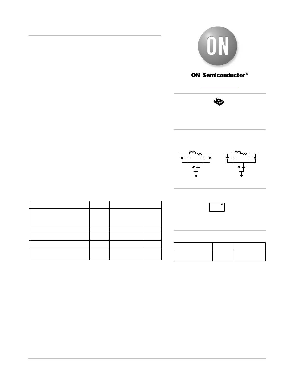
BLOCK DIAGRAM
Filter#1
WLCSP5
FC SUFFIX
CASE 567MA
A3
C1
Filter#2
C3
Applications
• Mobile Phones
MAXIMUM RATINGS (T
Rating
ESD Discharge IEC61000−4−2
Contact Discharge
Air Discharge
RMS Current per Line I
Operating Temperature Range T
Storage Temperature Range T
Lead Solder Temperature
(10 second duration)
Stresses exceeding those listed in the Maximum Ratings table may damage the
device. If any of these limits are exceeded, device functionality should not be
assumed, damage may occur and reliability may be affected.
= 25°C)
A
Symbol Value Unit
V
Line
T
stg
pp
J
L
30
30
350 mA
−40 to +125 °C
−55 to +150 °C
260 °C
kV
GND B1
GND B1
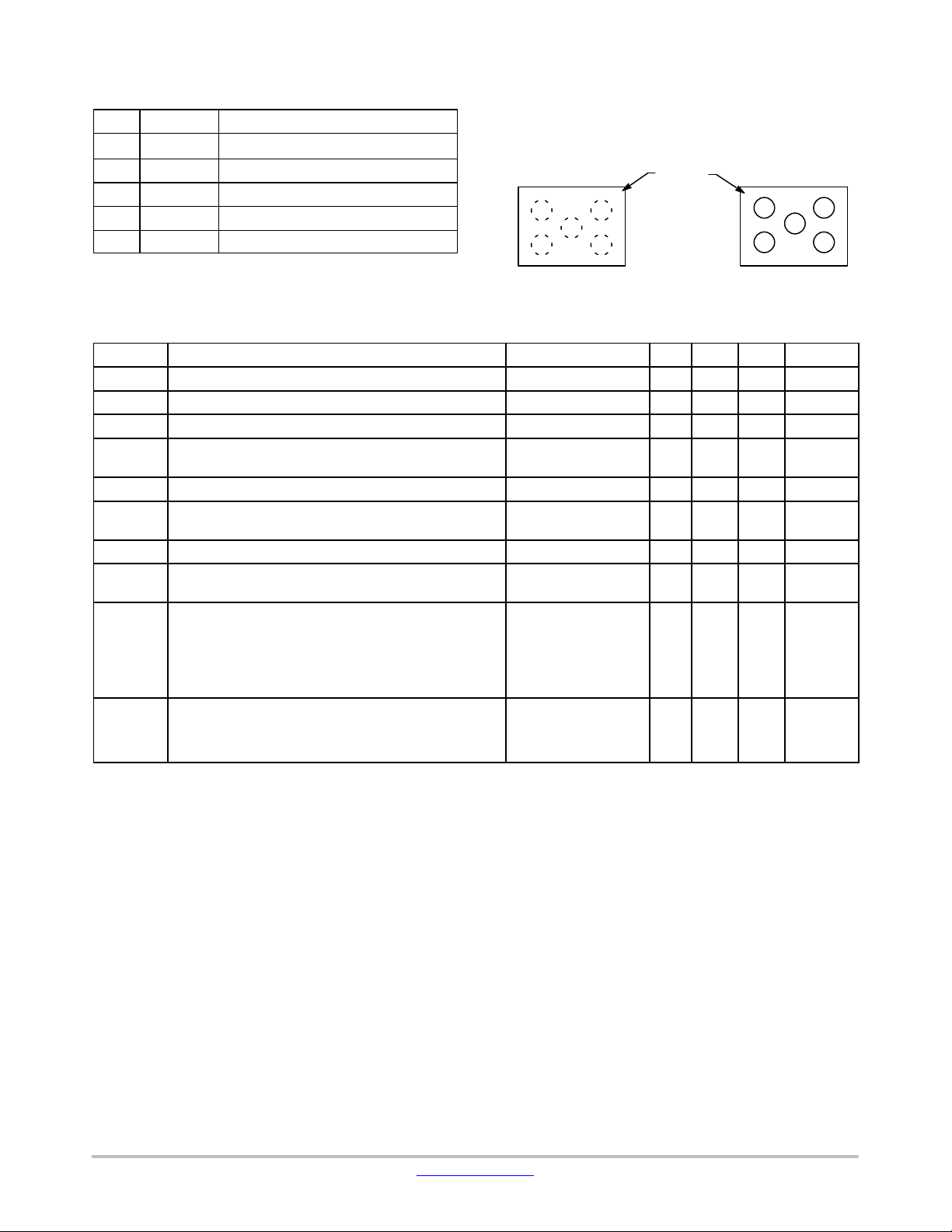
MARKING DIAGRAM
ATM
AT = Specific Device Code
M = Date Code
ORDERING INFORMATION
Device Package Shipping
CSPEMI204FCTAG WLCSP5
(Pb−Free)
†For information on tape and reel specifications,
including part orientation and tape sizes, please
refer to our Tape and Reel Packaging Specification
Brochure, BRD8011/D.
5000 / Tape &
Reel
†
© Semiconductor Components Industries, LLC, 2015
August, 2015 − Rev. 0
1 Publication Order Number:
CSPEMI204/D
Page 2
CSPEMI204
Table 1. PIN DESCRIPTIONS
Pin Name Description
A1 Filter #1 Filter #1 Input/Output
C1 Filter #1 Filter #1 Input/Output
A3 Filter #2 Filter #2 Input/Output
C3 Filter #2 Filter #2 Input/Output
B2 GND Device Ground
(Bumps Down View)
PACKAGE/PINOUT DIAGRAMS
Top View
Orientation
+
Marking
1
2
3
A
B
C
AT
Bottom View
(Bumps Up View)
+
A1 C1
B2
A3 C3
WLCSP5 Package
Table 2. ELECTRICAL OPERATING CHARACTERISTICS (T
Symbol
V
RWM
V
BR
I
LEAK
R
CH
C
t
f
3dB
f
3dB
F
atten
V
ESD
Working Voltage 3.0 V
Breakdown Voltage I
Channel Leakage Current
Channel Resistance
(Pins A1 – A3, C1 – C3)
Line Capacitance V
Cutoff Frequency 450 W Source and
Cutoff Frequency 50 W Termination
Stop Band Attenuation @ 700 MHz
Insystem ESD Withstand Voltage
a) Contact discharge per IEC 6100042 standard, Level 4
Parameter Test Conditions Min Typ Max Unit
= 25°C unless otherwise noted)
A
= 1 mA; (Note 4) 6.0 V
T
V
= 3.0 V, GND = 0 V
IN
= 0 V, f = 1 MHz 185 250 315 pF
R
10 kW Load Termination
@ 900 MHz
(Notes 1 and 2)
2.0 MHz
25 MHz
40
47
±30
400 nA
3.0
W
dB
kV
(External Pins)
b) Contact discharge per IEC 6100042 standard, Level 1
±30
(Internal Pins)
V
TLP Clamping Voltage Forward I
CL
Forward I
Forward I
Forward I
PP
PP
PP
PP
= 8 A
= 16 A
= ±8 A
= ±16 A
9.8
11.5
−9.7
−11.7
V
Product parametric performance is indicated in the Electrical Characteristics for the listed test conditions, unless otherwise noted. Product
performance may not be indicated by the Electrical Characteristics if operated under different conditions.
1. Standard IEC61000−4−2 with C
2. These measurements performed with no external capacitor.
Discharge
= 150 pF, R
3. TVS devices are normally selected according to the working peak reverse voltage (V
or continuous peak operating voltage level.
is measured at pulse test current IT.
4. V
BR
Discharge
= 330, GND grounded.
), which should be equal to or greater than the DC
RWM
www.onsemi.com
2
Page 3
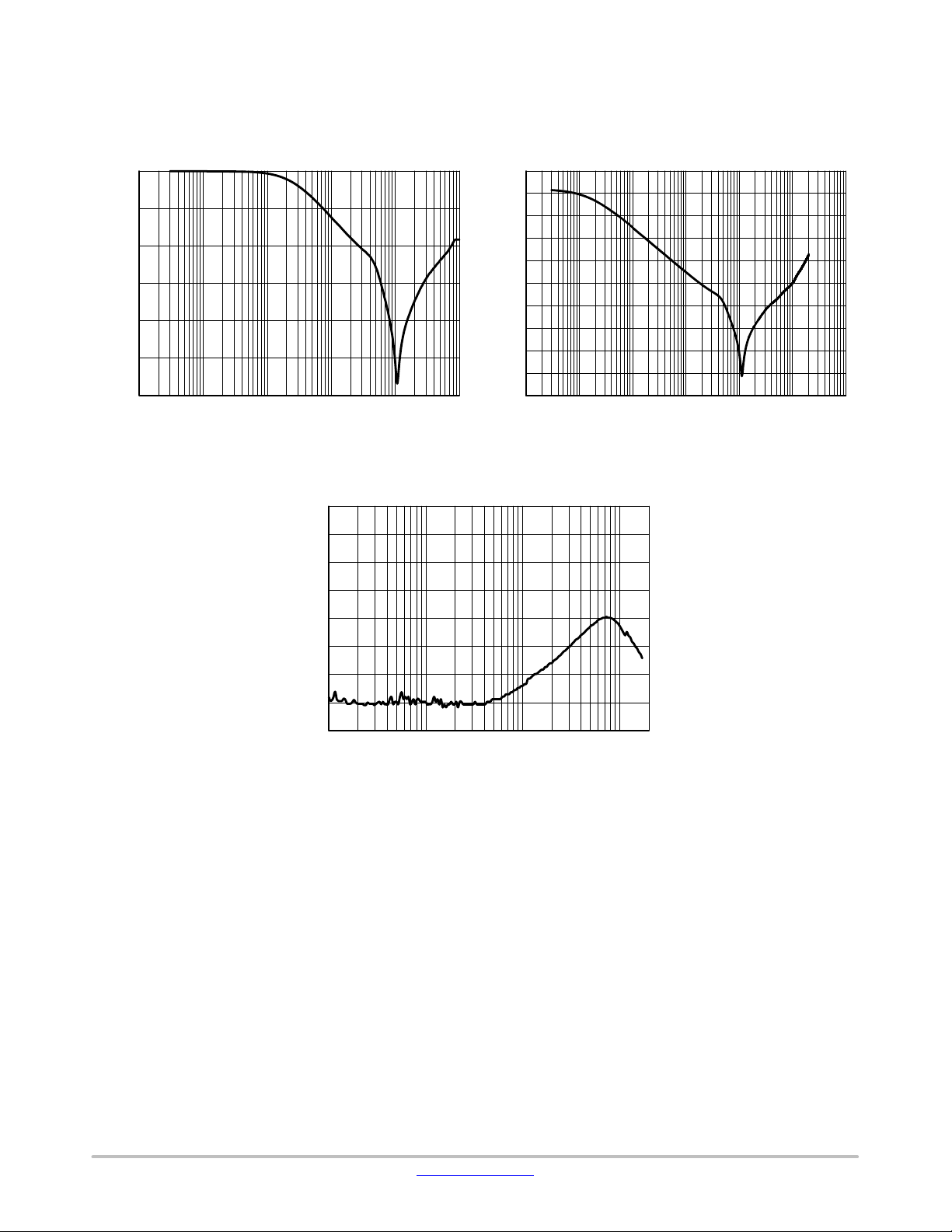
Typical Filter Performance
0
S21 (dB)
pp
11
0
CSPEMI204
PERFORMANCE INFORMATION
−10
−20
−30
−40
−50
−60
1.E+05 1.E+06
1.E+07 1.E+08 1.E+09 1.E+10
FREQUENCY (Hz)
Figure 1. Typical Insertion Loss (50 W
Termination)
−80
−85
−90
−95
−100
−10
−20
−30
−40
−50
S21 (dB)
−60
−70
−80
−90
−100
1.E+05 1.E+06 1.E+10
1.E+07 1.E+08 1.E+09 1.E+
FREQUENCY (Hz)
Figure 3. Typical Insertion Loss (450 W Source
and 10 kW Load Termination)
−105
THD+N (dB)
−110
−115
−120
20 200 2000 20000
FREQUENCY (Hz)
Figure 2. Typical THD+N at 1.8 V
www.onsemi.com
3
Page 4

CSPEMI204
IEC 61000−4−2 Spec.
Test Volt-
Level
age (kV)
1 2 7.5 4 2
2 4 15 8 4
3 6 22.5 12 6
4 8 30 16 8
ESD Gun
First Peak
Current
(A)
Current at
30 ns (A)
TVS
50 W
Cable
IEC61000−4−2 Waveform
I
peak
Current at
60 ns (A)
Figure 4. IEC61000−4−2 Spec
100%
90%
I @ 30 ns
I @ 60 ns
10%
Oscilloscope
50 W
tP = 0.7 ns to 1 ns
Figure 5. Diagram of ESD Clamping Voltage Test Setup
The following is taken from Application Note
AND8308/D − Interpretation of Datasheet Parameters
for ESD Devices.
ESD Voltage Clamping
For sensitive circuit elements it is important to limit the
voltage that an IC will be exposed to during an ESD event
to as low a voltage as possible. The ESD clamping voltage
is the voltage drop across the ESD protection diode during
an ESD event per the IEC61000−4−2 waveform. Since the
IEC61000−4−2 was written as a pass/fail spec for larger
systems such as cell phones or laptop computers it is not
clearly defined in the spec how to specify a clamping voltage
at the device level. ON Semiconductor has developed a way
to examine the entire voltage waveform across the ESD
protection diode over the time domain of an ESD pulse in the
form of an oscilloscope screenshot, which can be found on
the datasheets for all ESD protection diodes. For more
information on how ON Semiconductor creates these
screenshots and how to interpret them please refer to
AND8307/D.
www.onsemi.com
4
Page 5

CSPEMI204
25
20
15
10
TLP CURRENT (A)
5
0
01412246 108
VC, VOLTAGE (V)
Figure 6. Positive TLP I−V Curve (Preliminary)
NOTE: TLP parameter: Z
stress level calculated at the secondary peak of the IEC 61000−4−2 waveform at t = 30 ns with 2 A/kV. See TLP description
below for more information.
= 50 W, tp = 100 ns, tr = 300 ps, averaging window: t1 = 30 ns to t2 = 60 ns. V
0
Transmission Line Pulse (TLP) Measurement
Transmission Line Pulse (TLP) provides current versus
voltage (I−V) curves in which each data point is obtained
from a 100 ns long rectangular pulse from a charged
transmission line. A simplified schematic of a typical TLP
system is shown in Figure 8. TLP I−V curves of ESD
protection devices accurately demonstrate the product’s
ESD capability because the 10s of amps current levels and
under 100 ns time scale match those of an ESD event. This
is illustrated in Figure 9 where an 8 kV IEC 61000−4−2
current waveform is compared with TLP current pulses at
8 A and 16 A. A TLP I−V curve shows the voltage at which
the device turns on as well as how well the device clamps
voltage over a range of current levels.
−25
−20
−15
−10
TLP CURRENT (A)
−5
0
0 −14−12−10−2 −4 −6 −8
VC, VOLTAGE (V)
Figure 7. Negative TLP I−V Curve (Preliminary)
is the equivalent voltage
IEC
L
Attenuator
S
÷
50 W Coax
Cable
10 MW
V
C
Figure 8. Simplified Schematic of a Typical TLP
System
I
M
V
Oscilloscope
50 W Coax
Cable
M
DUT
Figure 9. Comparison Between 8 kV IEC 61000−4−2 and 8 A and 16 A TLP Waveforms
www.onsemi.com
5
Page 6

MECHANICAL CASE OUTLINE
PACKAGE DIMENSIONS
SCALE 4:1
WLCSP5, 1.26x0.89
CASE 567MA
ISSUE O
DATE 07 JUL 2015
REFERENCE
2X
2X
NOTE 3
0.05
PIN A1
0.05 C
5X
C
0.10 C
0.10 C
0.10 C
A1
b
A0.10 BC
E
TOP VIEW
SIDE VIEW
C
B
A
123
BOTTOM VIEW
e/2
e
A
B
D
A2
A
NOTES:
1. DIMENSIONING AND TOLERANCING PER ASME
Y14.5M, 1994.
2. CONTROLLING DIMENSION: MILLIMETERS.
3. COPLANARITY APPLIES TO SPHERICAL
CROWNS OF SOLDER BALLS.
4. DIMENSION b IS MEASURED AT THE MAXIMUM
BALL DIAMETER PARALLEL TO DATUM C.
MILLIMETERS
DIMAMIN MAX
−−−
A1
A2 0.255 REF
b 0.235 0.295
D 1.26 BSC
E
e 0.50 BSC
e1 0.435 BSC
0.50
0.18 0.22
0.89 BSC
GENERIC
MARKING DIAGRAM*
XXM
XX = Specific Device Code
M = Date Code
e1
C
SEATING
PLANE
*This information is generic. Please refer to
device data sheet for actual part marking.
Pb−Free indicator, “G” or microdot “ G”,
may or may not be present.
RECOMMENDED
SOLDERING FOOTPRINT*
PACKAGE
A1
OUTLINE
5X
0.27
0.87
PITCH
0.50
PITCH
DIMENSIONS: MILLIMETERS
*For additional information on our Pb−Free strategy and soldering
details, please download the ON Semiconductor Soldering and
Mounting Techniques Reference Manual, SOLDERRM/D.
DOCUMENT NUMBER:
DESCRIPTION:
ON Semiconductor and are trademarks of Semiconductor Components Industries, LLC dba ON Semiconductor or its subsidiaries in the United States and/or other countries.
ON Semiconductor reserves the right to make changes without further notice to any products herein. ON Semiconductor makes no warranty, representation or guarantee regarding
the suitability of its products for any particular purpose, nor does ON Semiconductor assume any liability arising out of the application or use of any product or circuit, and specifically
disclaims any and all liability, including without limitation special, consequential or incidental damages. ON Semiconductor does not convey any license under its patent rights nor the
rights of others.
98AON00069G
WLCSP5, 1.26X0.89
Electronic versions are uncontrolled except when accessed directly from the Document Repository.
Printed versions are uncontrolled except when stamped “CONTROLLED COPY” in red.
PAGE 1 OF 1
© Semiconductor Components Industries, LLC, 2019
www.onsemi.com
Page 7

ON Semiconductor and are trademarks of Semiconductor Components Industries, LLC dba ON Semiconductor or its subsidiaries in the United States and/or other countries.
ON Semiconductor owns the rights to a number of patents, trademarks, copyrights, trade secrets, and other intellectual property. A listing of ON Semiconductor ’s product/patent
coverage may be accessed at www.onsemi.com/site/pdf/Patent−Marking.pdf
ON Semiconductor makes no warranty, representation or guarantee regarding the suitability of its products for any particular purpose, nor does ON Semiconductor assume any liability
arising out of the application or use of any product or circuit, and specifically disclaims any and all liability, including without limitation special, consequential or incidental damages.
Buyer is responsible for its products and applications using ON Semiconductor products, including compliance with all laws, regulations and safety requirements or standards,
regardless of any support or applications information provided by ON Semiconductor. “Typical” parameters which may be provided in ON Semiconductor data sheets and/or
specifications can and do vary in different applications and actual performance may vary over time. All operating parameters, including “Typicals” must be validated for each customer
application by customer’s technical experts. ON Semiconductor does not convey any license under its patent rights nor the rights of others. ON Semiconductor products are not
designed, intended, or authorized for use as a critical component in life support systems or any FDA Class 3 medical devices or medical devices with a same or similar classification
in a foreign jurisdiction or any devices intended for implantation in the human body. Should Buyer purchase or use ON Semiconductor products for any such unintended or unauthorized
application, Buyer shall indemnify and hold ON Semiconductor and its officers, employees, subsidiaries, affiliates, and distributors harmless against all claims, costs, damages, and
expenses, and reasonable attorney fees arising out of, directly or indirectly, any claim of personal injury or death associated with such unintended or unauthorized use, even if such
claim alleges that ON Semiconductor was negligent regarding the design or manufacture of the part. ON Semiconductor is an Equal Opportunity/Affirmative Action Employer. This
literature is subject to all applicable copyright laws and is not for resale in any manner.
. ON Semiconductor reserves the right to make changes without further notice to any products herein.
PUBLICATION ORDERING INFORMATION
LITERATURE FULFILLMENT:
Email Requests to: orderlit@onsemi.com
ON Semiconductor Website: www.onsemi.com
TECHNICAL SUPPORT
North American Technical Support:
Voice Mail: 1 800−282−9855 Toll Free USA/Canada
Phone: 011 421 33 790 2910
Europe, Middle East and Africa Technical Support:
Phone: 00421 33 790 2910
For additional information, please contact your local Sales Representative
◊
www.onsemi.com
1
 Loading...