

Page 1
查询CS51227供应商
CS51227
Enhanced Voltage Mode
PWM Controller
The CS51227 is a fixed frequency, single output PWM controller
using feed forward voltage mode control. Feed forward control
provides superior line regulation and line transient response. This
PWM controller has been optimized for high frequency primary side
control operation. It has undervoltage lockout with 4.7 V start up
voltage and 75 µA start up current. One external capacitor can
program the switching frequency up to 1.0 MHz. The protection
features include pulse–by–pulse current limit with leading edge
blanking and thermal shutdown. The CS51227 is available in 8 lead
SO narrow surface mount package.
http://onsemi.com
8
1
SO–8
D SUFFIX
CASE 751
Features
• 1.0 MHz Frequency Capability
• 4.7 V Start–Up Voltage
• Fixed Frequency Voltage Mode Operation with Feed Forward
• Undervoltage Lockout
• 75 µA Start–Up Current
• Thermal Shutdown
• 1.0 A Sink/Source Gate Drive
• Pulse–By–Pulse Current Limit with Leading Edge Blanking
• 50 ns GATE Rise and Fall Time (1.0 nF Load)
• Maximum Duty Cycle Over 85%
• Programmable Volt–Second Clamp
PIN CONNECTIONS AND
MARKING DIAGRAM
1
GATE
SENSE
CT
A = Assembly Location
WL, L = Wafer Lot
YY, Y = Year
WW, W = Work Week
ORDERING INFORMATION
Device Package Shipping
CS51227ED8 SO–8 95 Units/Rail
CS51227EDR8 SO–8
ALYW
8
51227
V
CC
GNDI
COMPFF
V
FB
2500 Tape & Reel
Semiconductor Components Industries, LLC, 2001
April, 2001 – Rev. 7
1 Publication Order Number:
CS51227/D
Page 2
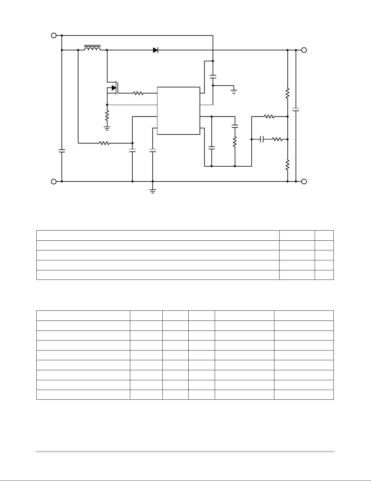
5.0 V
6.8 µH
FS70VSJ–03
0.1
B320DICT
GATE
CS51227
V
CC
12 V/ 2.0 A
0.1 µF
1.0 k
GND
COMP
CS51227
V
FB
2700 pF
100 pF
9.1 k
5.6 nF
51 k
+
22 µF × 4
300
+
22 µF × 2
9.31 k
0.025
330 pF1.0 nF
I
SENSE
FF
CT
110
GND
GND
Figure 1. Applications Diagram, 5.0 V to 12 V/2.0 A Boost Converter
MAXIMUM RATINGS*
Rating Value Unit
Operating Junction Temperature, T
Storage Temperature Range, T
J
S
ESD Susceptibility (Human Body Model) 2.0 kV
Lead Temperature Soldering: Reflow: (SMD styles only) (Note 1) 230 peak °C
1. 60 second maximum above 183°C.
*The maximum package power dissipation must be observed.
150 °C
–65 to +150 °C
MAXIMUM RATINGS
Pin Name Pin Symbol V
Gate Drive Output GATE 20 V –0.3 V 1.0 A Peak, 200 mA DC 1.0 A Peak, 200 mA DC
Current Sense Input I
Timing Capacitor CT 6.0 V –0.3 V 1.0 mA 10 mA
Feed Forward FF 6.0 V –0.3 V 1.0 mA 25 mA
Error Amp Output COMP 6.0 V –0.3 V 10 mA 20 mA
Feedback Voltage V
Power Supply V
Ground GND N/A N/A 1.0 A Peak, 200 mA DC N/A
SENSE
FB
CC
MAX
V
MIN
I
SOURCE
I
SINK
6.0 V –0.3 V 1.0 mA 1.0 mA
6.0 V –0.3 V 1.0 mA 1.0 mA
20 V –0.3 V 10 mA 1.0 A Peak, 200 mA DC
http://onsemi.com
2
Page 3
CS51227
ELECTRICAL CHARACTERISTICS: (–40°C < T
C
= 390 pF; unless otherwise specified.)
T
Characteristic
< 85°C, –40°C < TJ < 125°C, 4.7 V < VCC < 18 V
A
Test Conditions Min Typ Max Unit
Start/Stop Voltages
Start Threshold – 4.4 4.5 4.7 V
Stop Threshold – 3.2 3.8 4.2 V
Hysteresis Start – Stop 300 700 1400 mV
ICC @ Startup VCC < UVL Start Threshold – 38 75 µA
Supply Current
ICC Operating No Load – 10 16 mA
Overcurrent Protection
Overcurrent Threshold Ramp I
I
to GATE Delay VFB = 0.5 V (no blanking) – 60 125 ns
SENSE
SENSE
0.27 0.30 0.33 V
Error Amp
Reference Voltage VFB connected to COMP 1.234 1.263 1.285 V
VFB Input Current VFB = 1.25 V – 1.3 2.0 µA
Open Loop Gain Note 2 60 90 – dB
Unity Gain Bandwidth Note 2 1.5 2.5 – MHz
COMP Sink Current COMP = 1.4 V, VFB = 1.45 V 3.0 12 32 mA
COMP Source Current COMP = 1.4 V, VFB = 1.15 V 1.0 1.7 2.4 mA
COMP High Voltage VFB = 1.15 V 2.8 3.1 3.4 V
COMP Low Voltage VFB = 1.45 V 75 150 300 mV
PSRR Freq = 120 Hz, Note 2 60 85 – dB
Oscillator
Frequency Accuracy – 200 235 270 kHz
Max Duty Cycle – 85 90 95 %
Peak Voltage Note 2 1.99 2.05 2.11 V
Valley Clamp Voltage – 0.90 0.95 1.00 V
Valley Voltage Note 2 0.90 0.95 1.00 V
Discharge Current – 0.85 1.00 1.15 mA
Charge Current – 95 115 135 µA
Gate Driver
High Saturation Voltage VCC – V
Low Saturation Voltage V
GATE
, VCC = 10 V, I
GATE
, I
= 150 mA – 1.2 1.5 V
SINK
= 150 mA – 1.5 2.0 V
SOURCE
High Voltage Clamp – 11 13.5 16 V
Output UVL Leakage V
= 0 V – 1.0 50 µA
GATE
Rise Time 1.0 nF Load, VCC = 18 V, 1.0 V < VO < 9.0 V – 32 50 ns
Fall Time 1.0 nF Load, VCC = 18 V, 9.0 V < VO < 1.0 V – 25 50 ns
Max GATE Voltage @ UVL I
= 100 µA 0.4 0.7 1.5 V
LOAD
2. Guaranteed by design, not 100% tested in production.
http://onsemi.com
3
Page 4
CS51227
ELECTRICAL CHARACTERISTICS: (continued) (–40°C < T
C
= 390 pF; unless otherwise specified.)
T
< 85°C, –40°C < TJ < 125°C, 4.7 V < VCC < 18 V
A
Characteristic UnitMaxTypMinTest Conditions
Feed Forward (FF)
Discharge Voltage IFF = 2.0 mA – 0.3 0.7 V
Discharge Current FF = 1.0 V 2.0 16 30 mA
FF to GATE Delay – 50 75 125 ns
FF Max VOltage VFB = 1.15 V 1.7 1.8 1.9 V
Blanking
Blanking Time – 50 150 250 ns
COMP Blanking Disable Threshold VFB < 1.0 V 2.8 3.0 3.3 V
Thermal Shutdown
Thermal Shutdown
Note 3 125 150 180 °C
Thermal Hysteresis Note 3 5.0 10 15 °C
3. Guaranteed by design, not 100% tested in production.
PACKAGE PIN DESCRIPTION
PACKAGE LEAD #
SO–8
1 GATE External power switch driver with 1.0 A peak capability. Rail–to–rail output
2 I
3 FF PWM ramp.
4 CT Timing capacitor CT determines oscillator frequency.
5 V
6 COMP Error amplifier output.
7 GND Ground.
8 V
LEAD SYMBOL FUNCTION
occurs when the capacitive load is between 470 pF and 10 nF.
SENSE
FB
CC
Current sense comparator input.
Feedback voltage input. Connected to the error amplifier inverting input.
Supply voltage.
http://onsemi.com
4
Page 5
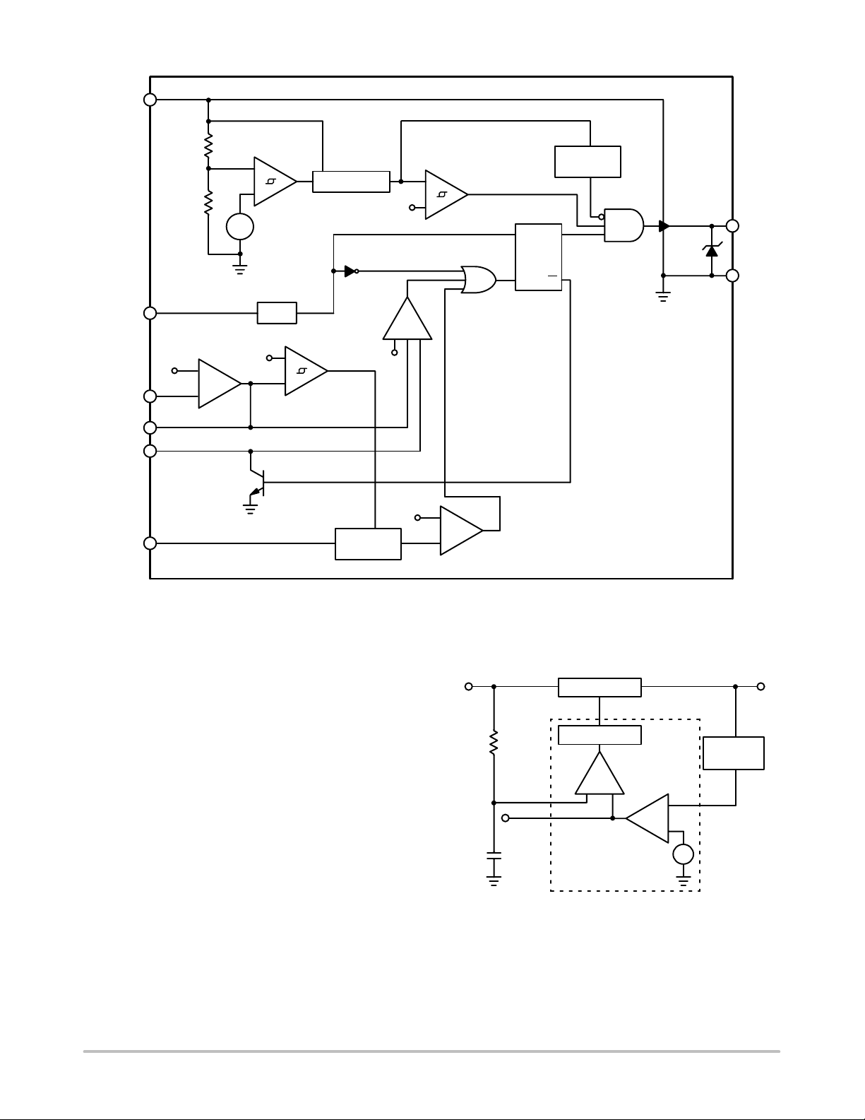
V
CC
4.7 – 18 V
CT
V
FB
COMP
FF
1.263 V
EAMP
+
–
+
–
+
–
UV Lockout
Start/Stop
OSC
3.0 V
CS51227
3.3 V
V
OK
REF
V
= 3.3 V
REF
3.1 V
PWM
COMP
+
–
Blank
Disable
1.8 V
+
–
G2
–+–
SRQ
V
REF
Thermal
Shutdown
Q
G1
Low Sat
Gate Driver
GATE
13.5 V
GND
FF Discharge
0.3 V
I
SENSE
150 ns
Blank
Figure 2. Block Diagram
THEORY OF APPLICATION
THEORY OF OPERATION
Feed Forward Voltage Mode Control
In conventional voltage mode control, the ramp signal is
fixed and often generated by the oscillator. The output
voltage is the only feedback path for regulation against load
and line variations. Feed forward voltage mode uses the
ramp signal driven by the input line, as shown in Figure 3.
Therefore, the ramp signal responds immediately to line
change. At the start of each switch cycle, the FF pin
capacitor is charged up through a resistor connected to the
input line. Meanwhile, the Gate output is turned on to drive
an external power switching device. When the FF pin
voltage reaches the error amplifier output V
COMP
, the PWM
comparator turns off the Gate and the FF pin capacitor is
quickly discharged by an internal current source.
+
I
LIM
–
V
IN
R
COMP
C
FF
Power Stage
GATE
Latch & Driver
PWM
Error
Amplifier
–
+
Figure 3. Feed Forward Voltage Mode Control
+
–
Feedback
Network
FB
V
OUT
http://onsemi.com
5
Page 6
CS51227
V
OUT
V
COMP
FF
V
IN
C
T
GATE
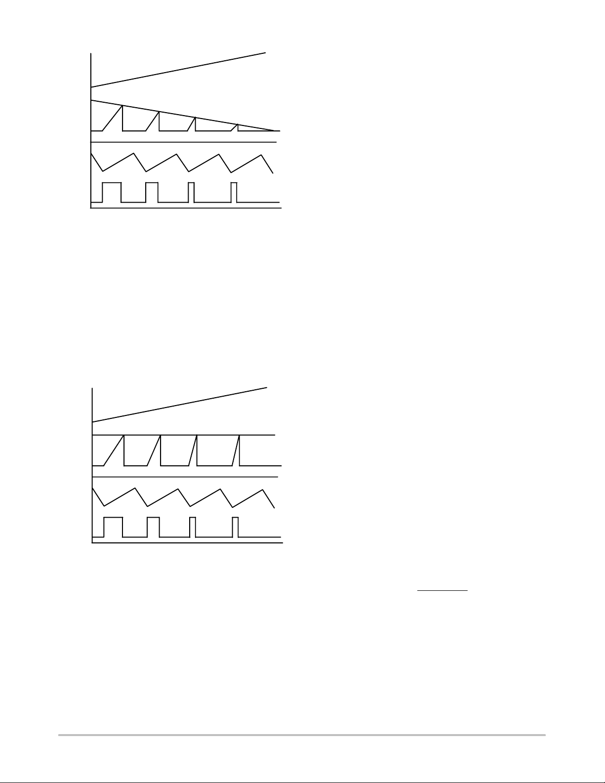
Figure 4. Pulse Width Modulated By Output
Current With Constant Input Voltage
Overall, the dynamics of the duty cycle are controlled by
both input and output voltages. As shown in Figure 4, an
elevated output voltage reduces V
through the error
COMP
amplifier. This in turn decreases the duty cycle and corrects
the deviation of the output voltage. For line variation, the
ramp signal responds immediately, which provides much
improved line transient response. The delay associated with
the power stage and feedback path has been totally avoided.
As an example, shown in Figure 5, when the input line goes
up, the slope of the ramp signal increases, reducing duty
cycle to counteract the change.
V
OUT
V
COMP
FF
V
IN
C
T
GATE
Figure 5. Pulse Width Modulated By Input
Voltage With Constant Output Voltage
The feed forward feature can also be employed to
implement volt–second clamping, which limits the
maximum product of input voltage and turn on time. This
clamp is used in circuits, such as Forward and Flyback
converters, to prevent the transformer from saturating. The
calculation for volt–second clamping is presented in the
Design Guidelines section.
Powering the IC & UVL
The internal logic monitors the supply voltage to ensure
the controller has enough operating headroom. The V
REF
block provides power to the controller’s logic. The
V
REF(OK)
and flags a fault if V
comparator monitors the internal 3.3 V V
falls below 3.1 V.
REF
REF
line
The Undervoltage Lockout (UVL) comparator has two
voltage references; the start and stop thresholds. During
power–up, the UVL comparator disables V
REF
(which
in–turn disables the entire IC) until the controller reaches its
VCC start threshold. During power–down, the UVL
comparator allows the controller to operate until the V
CC
stop threshold is reached. The CS51227 requires only 50 µA
during startup. During low VCC and abnormal operation
conditions, the output stage is held at a low level, low
impedance state.
Current Sense and Over Current Protection
The I
pulse current limit. When the I
pin monitors the switch current for pulse by
SENSE
pin voltage exceeds the
SENSE
internal threshold (0.3 V typical), the current limit
comparator immediately turns off the Gate signal. The Gate
will then stay off for the remainder of the cycle. Various
techniques, such as using current sensing resistor or current
transformer, a re w idely a dopted t o g enerate the c urrent s ignal.
The current sense signal is prone to leading edge spikes
caused by switching transitions. A RC low–pass filter can
effectively reduce the spikes a nd avoid p remature t riggering.
However, the low p ass f ilter will i nevitably c hange t he s hape
of the current pulse and also add cost. The CS51227 has
built–in leading edge blanking circuitry that blocks out the
first 150 ns (typ) of each current p ulse. T his f eature r emoves
the leading edge spikes without altering the current
waveform. Blanking is d isabled w hen the C OMP p in v oltage
exceeds 3.0 V (typ). This feature reduces the minimum duty
cycle during an output short or overload condition.
DESIGN GUIDELINES
Programming Oscillator Frequency
The switching frequency is set by the capacitor connected
to the C
pin. The CT pin voltage oscillates between 1.0 V
T
and 2.0 V. The ratio of the charge and discharge currents sets
the maximum duty cycle to be 90%. Use the following
equation to select C
,
T
C
T
9.027 10
7
f
s
where:
fs = Switching frequency
CT = Capacitance in pF
http://onsemi.com
6
Page 7
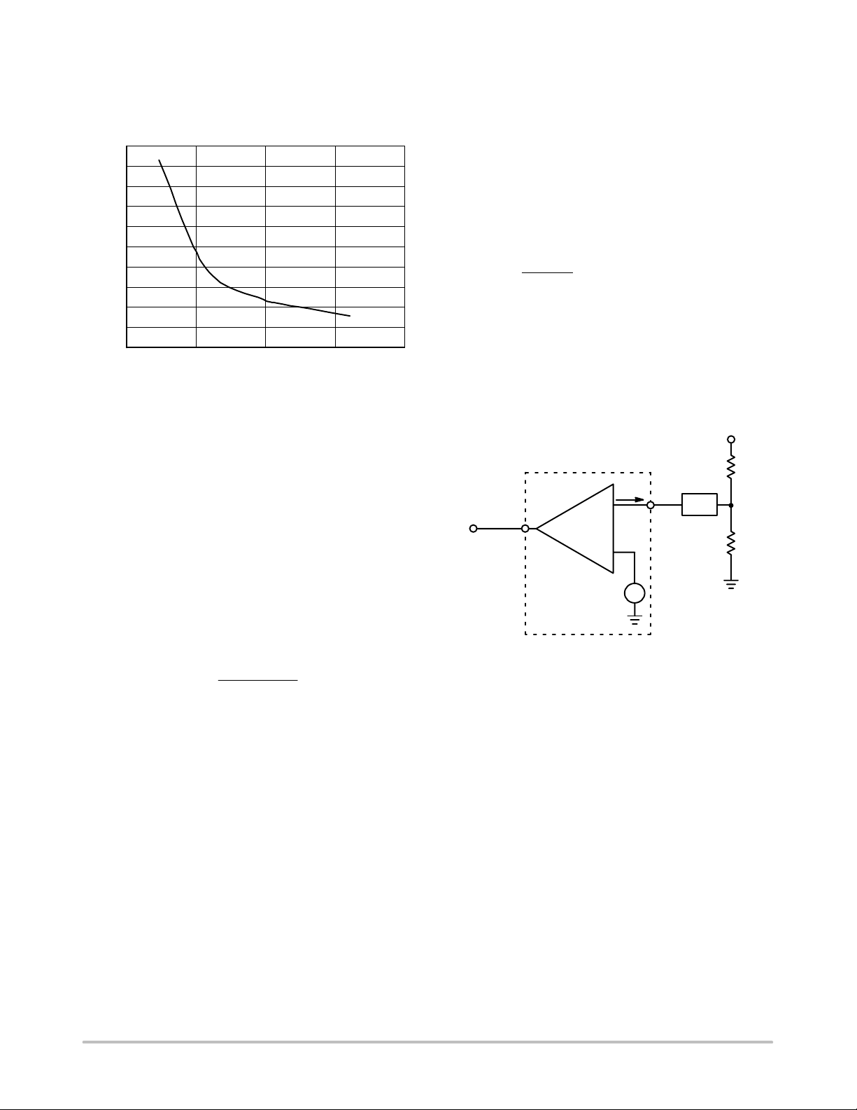
CS51227
When CT is less than 100 pF, parasitic capacitance
associated with the CT pin s tarts t o i mpact frequency a ccuracy.
Figure 6 shows typical oscillator frequency vs. CT value.
1000
900
800
700
600
500
400
300
200
Oscillator Frequency (kHz)
100
0
0 200 400 600 800
(pF)
C
T
Figure 6. Typical Performance Characteristics:
Oscillator Frequency vs. C
Component Selection for Feed Forward Ramp
T
FF discharge voltage and FF maximum voltage limit the
maximum voltage rise on the FF pin to 1.5 V typical. This
provides the volt–second clamp feature when the FF pin is
driven by the i nput l ine. I f t he l ine v oltage i s m uch g reater t han
the FF pin voltage, the charge current is approximately equal
to V
/R where R is the resistor connecting the FF pin and
IN
input line. The voltage second clamp then has the form of:
VIN TON 1.5 R C
FF
One can select RCFF to prevent magnetic devices from
saturating.
In a buck or forward converter, the error amplifier output
V
is equal to:
COMP
V
T
V
COMP
OUT
N R C
S
FF
0.3V
where:
N = Transformer turns ratio (use 1 for buck converter)
T
= Switching period
S
This equation shows that the error amplifier output is
independent of the input voltage. Therefore, the system does
not rely on the error amplifier to respond to line variations.
This excludes the delay associated with the error amplifier.
The line regulation is also greatly improved because both
error amplifier and ramp signal can contribute to DC
regulation.
Select Feedback Voltage Divider
As shown in Figure 7, the voltage divider output feeds the
FB pin which connects to the inverting input of the error
amplifier. The non–inverting input of the error amplifier is
connected to a 1.263 V reference voltage. The FB pin has an
input current which has to be taken into account for accurate
output voltage programming. The following equation can be
used to calculate the R1 and R2 value:
R2
R1 R2
V
OUT
1.263
∇
where ∇ is the correction factor
Ri R1R2 Ier
∇
Ri = DC resistance between the FB pin and the voltage
divider output, as shown in Figure 7.
Ier = FB pin input current, 1.3 µA typical.
V
OUT
R1
Ier
–
COMP
Figure 7. The Feedback Voltage Divider Design Has
to Consider the Error Amplifier Input Current
Thermal Management
Error
Amplifier
1.263 V
+
FB
Ri
R2
+
–
The CS51227 will enter thermal shutdown when the
junction (die surface) temperature exceeds 150°C, typical.
10°C typical thermal hysteresis will prevent part cycling, or
a “chattering” startup near the shutdown temperature.
Junction temperature is a function of the ambient
temperature, thermal resistance of the die and package, and
the power dissipated by the package and leads.
http://onsemi.com
7
Page 8

–Y–
–Z–
CS51227
PACKAGE DIMENSIONS
SO–8
D SUFFIX
CASE 751–07
–X–
A
58
B
1
S
0.25 (0.010)
4
G
C
SEATING
PLANE
0.10 (0.004)
H
D
0.25 (0.010) Z
M
Y
SXS
ISSUE V
NOTES:
1. DIMENSIONING AND TOLERANCING PER ANSI
Y14.5M, 1982.
2. CONTROLLING DIMENSION: MILLIMETER.
3. DIMENSION A AND B DO NOT INCLUDE MOLD
PROTRUSION.
M
M
Y
K
N
X 45
M
4. MAXIMUM MOLD PROTRUSION 0.15 (0.006) PER
SIDE.
5. DIMENSION D DOES NOT INCLUDE DAMBAR
PROTRUSION. ALLOWABLE DAMBAR
PROTRUSION SHALL BE 0.127 (0.005) TOTAL IN
EXCESS OF THE D DIMENSION AT MAXIMUM
MATERIAL CONDITION.
MILLIMETERS
DIMAMIN MAX MIN MAX
4.80 5.00 0.189 0.197
B 3.80 4.00 0.150 0.157
C 1.35 1.75 0.053 0.069
D 0.33 0.51 0.013 0.020
G 1.27 BSC 0.050 BSC
H 0.10 0.25 0.004 0.010
J
J 0.19 0.25 0.007 0.010
K 0.40 1.27 0.016 0.050
M 0 8 0 8
N 0.25 0.50 0.010 0.020
S 5.80 6.20 0.228 0.244
INCHES
PACKAGE THERMAL DATA
Parameter
R
Θ
JC
R
Θ
JA
ON Semiconductor and are trademarks of Semiconductor Components Industries, LLC (SCILLC). SCILLC reserves the right to make changes
without further notice to any products herein. SCILLC makes no warranty, representation or guarantee regarding the suitability of its products for any particular
purpose, nor does SCILLC assume any liability arising out of the application or use of any product or circuit, and specifically disclaims any and all liability,
including without limitation special, consequential or incidental damages. “Typical” parameters which may be provided in SCILLC data sheets and/or
specifications can and do vary in different applications and actual performance may vary over time. All operating parameters, including “Typicals” must be
validated for each customer application by customer’s technical experts. SCILLC does not convey any license under its patent rights nor the rights of others.
SCILLC products are not designed, intended, or authorized for use as components in systems intended for surgical implant into the body, or other applications
intended to support or sustain life, or for any other application in which the failure of the SCILLC product could create a situation where personal injury or
death may occur. Should Buyer purchase or use SCILLC products for any such unintended or unauthorized application, Buyer shall indemnify and hold
SCILLC and its officers, employees, subsidiaries, affiliates, and distributors harmless against all claims, costs, damages, and expenses, and reasonable
attorney fees arising out of, directly or indirectly, any claim of personal injury or death associated with such unintended or unauthorized use, even if such claim
alleges that SCILLC was negligent regarding the design or manufacture of the part. SCILLC is an Equal Opportunity/Affirmative Action Employer.
Typical 45 °C/W
Typical 165 °C/W
SO–8 Unit
PUBLICATION ORDERING INFORMATION
Literature Fulfillment:
Literature Distribution Center for ON Semiconductor
P.O. Box 5163, Denver, Colorado 80217 USA
Phone: 303–675–2175 or 800–344–3860 Toll Free USA/Canada
Fax: 303–675–2176 or 800–344–3867 Toll Free USA/Canada
Email: ONlit@hibbertco.com
N. American Technical Support: 800–282–9855 Toll Free USA/Canada
http://onsemi.com
JAPAN: ON Semiconductor, Japan Customer Focus Center
4–32–1 Nishi–Gotanda, Shinagawa–ku, Tokyo, Japan 141–0031
Phone: 81–3–5740–2700
Email: r14525@onsemi.com
ON Semiconductor Website: http://onsemi.com
For additional information, please contact your local
Sales Representative.
CS51227/D
8
 Loading...