

Page 1
查询CS51220供应商
CS51220
Feed Forward Voltage
Mode PWM Controller
with Programmable
Synchronization
CS51220 is a single output PWM Controller with switching
frequency up to 500 kHz. The feed forward voltage mode control
provides excellent line regulation for wide input range. This PWM
controller has a synchronization output allowing programmable phase
delay. For overcurrent protection, the “soft hiccup” technique
effectively limits the output current with maximum flexibility. In
addition, this device includes such features as: soft start,
pulse–by–pulse current limit, programmable foldback current limit,
volt–second clamping, maximum duty cycle, overvoltage and
undervoltage protection, and synchronization input. The CS51220 is
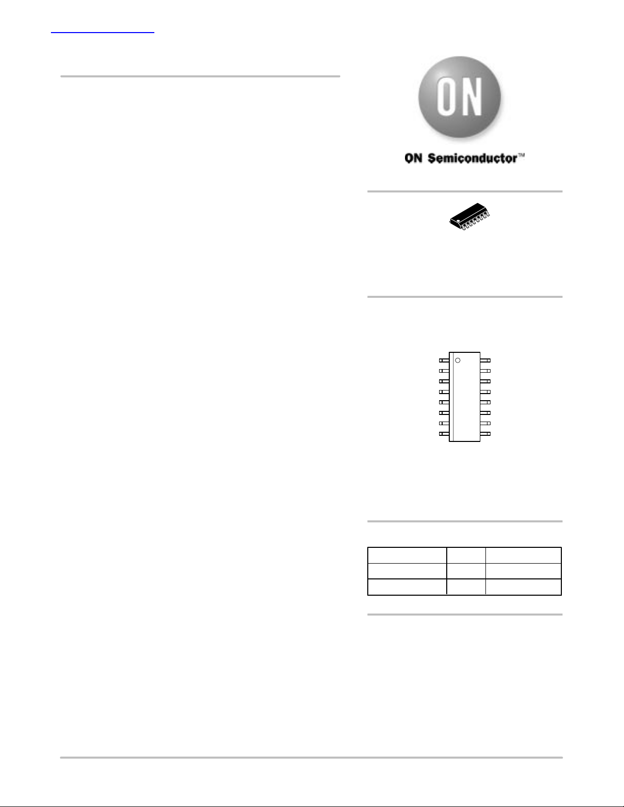
available in 16 SO narrow surface mount package.
Features
• Constant Frequency Feed Forward Voltage Mode Control
• Programmable Pulse by Pulse Overcurrent Limit
• Programmable Foldback Overcurrent Limit with Delay
• Soft Hiccup Overcurrent Protection with Programmable Foldback
• Frequency Synchronization Output with Programmable Phase Delay
• Synchronization Input to Higher or Lower Frequency
• Direct Connection to External Opto Isolators
• Logic Gate Output Signal
• Accurate Volt–Second Clamping
• Programmable Soft Start
• Logic Input to Disable IC
• Line Overvoltage and Undervoltage Monitoring
• 3.3 V 3% Reference Voltage Output
http://onsemi.com
16
1
SO–16
D SUFFIX
CASE 751B
PIN CONNECTIONS AND
MARKING DIAGRAM
1
O
GND
CC
REF
SET
SENSE
UV
A = Assembly Location
WL, L = Wafer Lot
YY, Y = Year
WW, W = Work Week
CS51220
AWLYWW
16
SYNCOV
V
SD
SSV
COMPV
FFI
DISABLEI
SYNCIOV
C
T
Semiconductor Components Industries, LLC, 2002
January , 2002 – Rev. 6
ORDERING INFORMATION
Device Package Shipping
CS51220ED16
CS51220EDR16
1 Publication Order Number:
SO–16
SO–16 2500 Tape & Reel
48 Units/Rail
CS51220/D
Page 2
CS51220
R4
D3
10
MMSD4148T1
L1
T1
D4
MMSD4148T1
100
R13
OUT
V
6.8 µH
D5B
MBRB2535CTL
70:1
R15
10 k
36
R14
C12
100 pF
3.3 V @
T2
5.0 A
C17
R23
330 µF
10
20:5
RTN
V
C18
330 µF
D5A
MBRB2535CTL
C12
680 pF
O
R21
R16
U4
10
C10
Q1
DD
V
OUT
DD
INA
V
0.1 µF
40.2 k
C13
100 pF
MTB20N20E
OUT
GNDGND
NCP4414
NC
200 V
C15
R20
R22
0.022 µF
C14
2.21 k
R19
R17
24.3 k
3.92 k
182
100 pF
U3
R18
1.0 K
U2
MOC213
TLV431ASNT1
R24
3.3 k
R3
10
C5
0.1 µF
U1
D2 15 V
R1
L2
100 k
C3
100 V
1.5 µF
36–72 V
1.0 µH
C1
0.2 µF
IN
V
100 V
R2
174 k
GND
Q2
MMFT1N10E
C4
C2
0.1 µF
MMSZ5245B
D1 9.1 V
MMSZ5239B
470 pF
500 V
CC
V
FF
V
SENSE
I
REF
R7
150 k
R5
10 k
O
SS
GND
SYNCI
SYNCO
CS51220
DISABLECOMP
ENABLE
SYNC IN
C7
1000 pF
R8
64.9 k
SYNC OUT
R11
510 k
R9
510 k
SET
OV
UV
I
VSDCTV
C8
390 pF
R6
7.5 k
C6
0.1 µF
R12
R10
11.8 k
15 k
C11
C9
1000 pF
1.0 µF
R23
220
R14
2.0 k
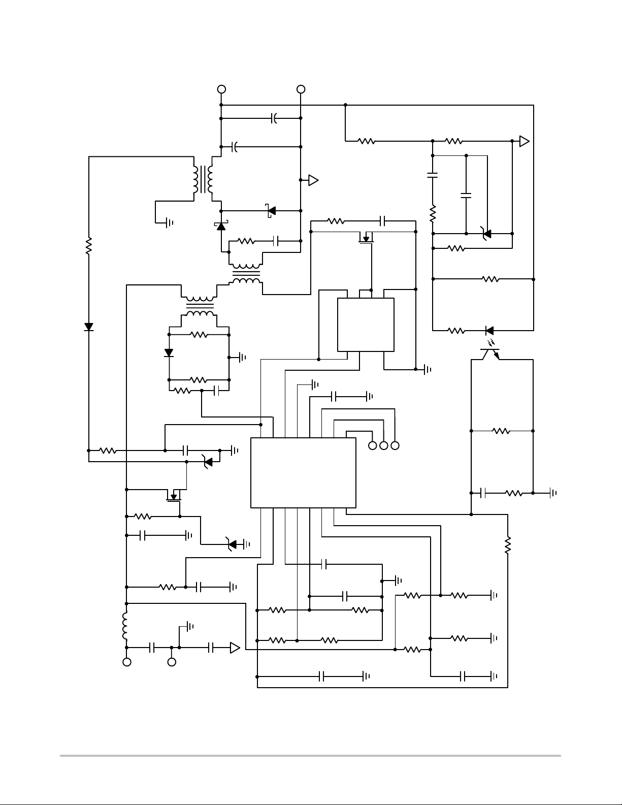
Figure 1. Application Diagram, 48 V to 3.3 V Converter
http://onsemi.com
2
Page 3
CS51220
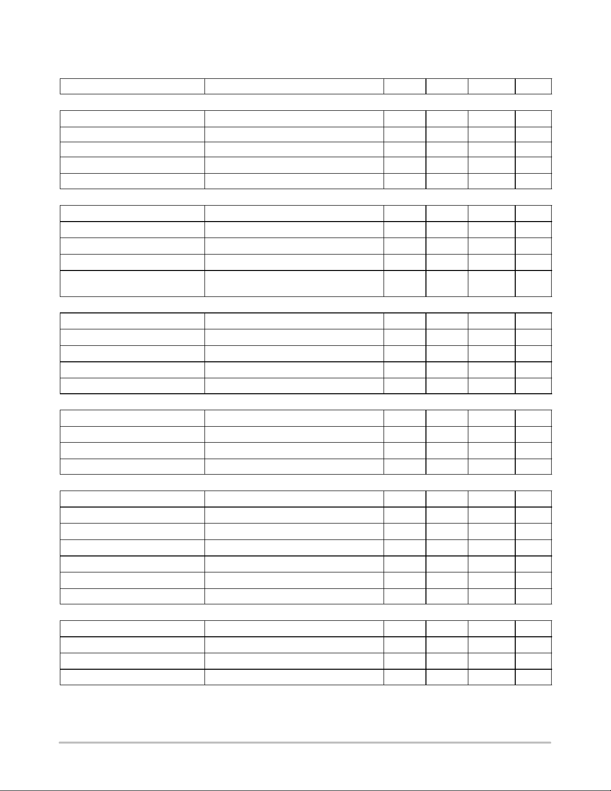
MAXIMUM RATINGS*
Rating Value Unit
Operating Junction Temperature, T
Storage Temperature Range, T
J
S
ESD Susceptibility (Human Body Model) 2.0 kV
Thermal Resistance, Junction–to–Case, R
Thermal Resistance, Junction–to–Ambient, R
Θ
JC
Θ
JA
Lead Temperature Soldering: Reflow: (SMD styles only) (Note 1) 230 peak °C
1. 60 second maximum above 183°C.
*The maximum package power dissipation must be observed.
MAXIMUM RATINGS
Pin Name Pin Symbol V
Gate Logic Output V
Current Sense Input I
Timing Capacitor C
O
SENSE
T
MAX
20 V –0.3 V 100 mA 100 mA
6.0 V –0.3 V 10 mA 10 mA
6.0 V –0.3 V 10 mA 10 mA
Feed Forward FF 6.0 V –0.3 V 10 mA 100 mA
Error Amp Output COMP 6.0 V –0.3 V 10 mA 10 mA
Feedback Voltage V
FB
6.0 V –0.3 V 10 mA 10 mA
Sync Input SYNCI 20 V –0.3 V 10 mA 10 mA
Power Down Input DISABLE 20 V –0.3 V 10 mA 10 mA
Undervoltage UV 6.0 V –0.3 V 10 mA 10 mA
Overvoltage OV 6.0 V –0.3 V 10 mA 10 mA
Current Set I
SET
6.0 V –0.3 V 10 mA 10 mA
Soft Start SS 6.0 V –0.3 V 10 mA 10 mA
Power Supply V
CC
20 V –0.3 V 10 mA 50 mA
Sync Output SYNCO 20 V –0.3 V 100 mA 100 mA
Reference Voltage V
Sync Delay V
REF
SD
6.0 V –0.3 V Internally Limited 10 mA
6.0 V –0.3 V 1.0 mA 1.0 mA
Ground GND N/A N/A 50 mA N/A
V
MIN
I
SOURCE
150 °C
–65 to +150 °C
28 °C/W
115 °C/W
I
SINK
http://onsemi.com
3
Page 4
CS51220
ELECTRICAL CHARACTERISTICS (–40°C < T
< 85°C; –40°C < TJ < 125°C; 4.7 V < VCC < 16 V; CT = 390 pF; unless
A
otherwise specified.)
Characteristic
Test Conditions Min Typ Max Unit
Supply Voltage/Current
Start Threshold – 4.0 4.4 4.7 V
Stop Threshold – 3.3 3.8 4.1 V
Hysteresis Start – Stop 400 600 1000 mV
ICC @ Startup VCC < UVL Start Threshold – – 500 µA
ICC Operating, Low V
ICC Operating, High V
CC
CC
4.7 V < VCC < 10 V – – 7.5 mA
10 V < VCC < 16 V – – 9.0 mA
Reference Voltage
Total Accuracy 0 mA < I
Line Regulation I
REF
Load Regulation 0 mA < I
< 2.0 mA 3.2 3.3 3.4 V
REF
= 2.0 mA – 6.0 20 mV
< 2.0 mA, VCC = 8.0 V – 6.0 15 mV
REF
Operating Life Shift T = 1000 Hrs., Note 2 – 4.0 20 mV
Fault Voltage – 2.8 2.95 3.1 V
V
OK Voltage – 2.9 3.05 3.2 V
REF
V
OK Hysteresis – 50 100 150 mV
REF
Current Limit V
= 2.5 V 2.0 25 65 mA
REF
Oscillator
Frequency Accuracy – 223 266 309 kHz
Temperature Stability Note 2 – 8.0 – %
Max Frequency Note 2 500 – – kHz
Duty Cycle – 80 85 90 %
Peak Voltage Note 2 1.9 2.0 2.1 V
Valley Voltage Note 2 0.85 0.90 0.98 V
Discharge Current VCT = 1.5 V 0.70 0.85 1.05 mA
Charge Current VCT = 1.5 V 127 150 183 µA
Synchronization
SYNCI Input Threshold f
SYNCI Input Resistance V
= 500 kHz 1.0 2.0 3.0 V
SYNC
= 0.5 50 150 250 kΩ
SYNC
Minimum Sync Frequency Reduction of nominal frequency. 25 – – %
Minimum Input Sync Pulse Width – – – 200 ns
SYNCO Output High R
= 5.0 k, VCC = 8.0 V 5.0 6.5 7.5 V
SYNCO
SYNCO Output Low Sink 1.0 mA, VSD = 2.5 V – 0.2 0.4 V
SYNCO Delay Time VCT = 1.5 V, Toggle V
SD
100 200 300 ns
2. Guaranteed by design. Not tested in production.
http://onsemi.com
4
Page 5
CS51220
ELECTRICAL CHARACTERISTICS (continued) (–40°C < T
< 85°C; –40°C < TJ < 125°C; 4.7 V < VCC < 16 V; CT = 390 pF; unless
A
otherwise specified.)
Characteristic UnitMaxTypMinTest Conditions
Output (continued)
High Saturation Voltage VCC – VO, V
Low Saturation Voltage VO – GND, I
Pull Down Resistance I
= 100 µA 25 50 75 kΩ
SINK
= 10 V, I
CC
= 100 µA – 0.7 1.0 V
SINK
= 100 µA – 1.4 2.0 V
SOURCE
Rise Time VCC = 10 V, 1.0 V < VO < 6.0 V; 50 pF load – 35 80 ns
Fall Time VCC = 10 V, 1.0 V < VO < 6.0 V; 50 pF load – 25 50 ns
Feed Forward
Discharge Voltage IFF = 2.0 mA 0.25 0.35 0.45 V
Discharge Current FF = 1.0 V 2.0 10 30 mA
FF to VO Delay Connect VO to FF, Measure min. pulse width. 50 75 150 ns
FF Clamp Voltage – 1.15 1.3 1.45 V
COMP Switch Off Voltage VFF = 0.2 V, Ramp down V
VFF = 0.2 V, Ramp down V
COMP
COMP
–40°C
0.8
1.4
1.4
1.6
1.7
1.7
Overcurrent Protection
Overcurrent Comparator DC Offset – 180 200 215 mV
I
Attenuation ∆V
SENSE
I
Input Resistance ∆V
SENSE
I
to GATE Delay V
SENSE
I
Foldback Sink Current I
SET
/∆V
ISET
ISENSE
= 0 V 40 82 150 kΩ
ISENSE
= 0.5 V 50 100 175 ns
ISET
= 0.5 V, SS = 1.5 V and I
SET
= 0.5 V 12 15 18 µA
SENSE
0.9 0.94 0.98 V/V
External Voltage Monitors
Overvoltage Threshold OV pin increasing 1.9 2.0 2.1 V
OV Hysteresis Current OV = 2.15 V 10 12.5 15 µA
Undervoltage Threshold UV pin decreasing 0.95 1.00 1.05 V
UV Hysteresis – 25 75 125 mV
Soft Start
Charge Current SS = 1.5 V 35 50 65 µA
Discharge Current SS = 1.5 V, UV = 1.5 V 4.0 5.0 7.0 µA
OC Delay Discharge Current SS = 2.85 V, I
SET
= 0.5, I
= 0.5 V 35 50 65 µA
SENSE
SS Clamp Voltage – 2.7 2.9 3.1 V
Discharge Voltage – 0.25 0.3 0.35 V
Soft Start Fault Voltage OV = 2.5 V or UV = 0.85 V – 0.1 0.2 V
Hiccup Delay Discharge Voltage – 0.08 0.1 0.12 V
Disable
DISABLE Input Threshold – 1.0 2.0 3.0 V
DISABLE Input Resistance V
DISABLE Operation Current, Low V
DISABLE Operation Current, High V
CC
CC
4.7 V < VCC < 10 V – – 800 µA
10 V < VCC < 16 V – – 1600 µA
= 0.5 V 50 150 250 kΩ
DISABLE
V
V
http://onsemi.com
5
Page 6

PACKAGE PIN #
16 Lead SO Narrow
1 V
2 GND Ground.
3 V
4 V
5 I
6 I
7 OV Overvoltage protection monitor.
8 UV Undervoltage protection monitor.
9 C
10 SYNCI By applying sync pulses to this pin, the IC can be synchro-
CS51220
PACKAGE PIN DESCRIPTION
PIN SYMBOL FUNCTION
O
CC
REF
SET
SENSE
T
Logic output connecting to external gate driver.
Supply Voltage.
3.3 V reference voltage output.
Voltage at this pin sets pulse–by–pulse overcurrent thresh-
old. When the I
time, a sink current is generated at this pin. Along with exter-
SENSE
exceeds I
SET
nal resistors, this current provides a foldback overcurrent
threshold. The sink current is disabled periodically for restart.
Current sense input for overcurrent protection.
Timing capacitor CT determines oscillator frequency.
nized to frequencies ranging from 25% slower to several
times faster than the internal oscillator frequency.
for a sustained period of
11 DISABLE Disable mode input pin. A voltage greater than 3.0 V turns off
the whole IC.
12 FF Feed forward input for PWM ramp. This pin allows external
connection to make the ramp adjustable to the input line.
13 COMP This pin carries feedback error signal from an external ampli-
fier. Internally, it connects to the PWM controller.
14 SS A capacitor is connected to this pin for Soft Start and soft
hiccup timing.
15 V
SD
The voltage at this pin programs the delay of the SYNCO
output in reference to the internal oscillator.
16 SYNCO Sync output.
http://onsemi.com
6
Page 7

V
CC
DISABLE
I
SENSE
I
SET
COMP
GND
FF
SYNCO
V
SD
SYNCI
C
CS51220
UVL Comparator
+
-
+
–
X0.94
+
–
200 mV
+
I
LIM
-
Ifoldback
1.3 V
SS
MIN
-
+
PWM COMP
OSC
T
= 3.3 V
V
REF
OC
Soft
Hiccup
CLK
RESET DOMINANT
S
R
-
+
V
REF
SS
Discharge
SS low
SS
Q
COMP
3.1 V
Off
SS
Clamp
RQ
Fault
Latch
Q
S
SET DOMINANT
-
+
OV COMP
UV COMP
SS low
SS
COMP
-
+
Charge
SS
Discharge
+
2.0 V
1.0 V
0.3 V
V
REF
SS
OV
UV
V
O
Figure 2. Block Diagram
http://onsemi.com
7
Page 8

CS51220
APPLICATIONS INFORMATION
THEORY OF OPERATION
Feed Forward Voltage Mode Control
Conventional voltage mode control uses a fixed ramp
signal for pulse width modulation, typically utilizing the
oscillator output as the ramp signal. Since the only feedback
signal comes from the output, this results in inferior line
regulation and audio susceptibility. A significant
improvement in line regulation and line transient response
can be achieved using Feed Forward Voltage Mode Control,
implemented using the CS51220 controller.
The enhancement comes from generating the ramp signal
using a pull–up resistor from the FF pin to the line voltage
and a capacitor to ground. The slope of the ramp then
depends on the line voltage. At the start of each switch cycle,
the capacitor connected to the FF pin is charged through the
resistor connected to the input voltage. Meanwhile, the V
pin goes high to turn on a power mosfet through an external
gate driver. When the rising FF pin exceeds the COMP input
pin, as driven through the regulation feedback loop, VO goes
low and turns off the external switch. Simultaneously, the FF
capacitor is quickly discharged and set for the next switching
cycle.
Overall, both input and output voltages control the
dynamics of the duty cycle. As illustrated in Figure 3, with
a fixed input voltage the output voltage is regulated solely
by the error amplifier. For example, an elevated output
voltage pulls down the COMP pin through an external error
amplifier. This in turn causes duty cycle to decrease. On the
another hand, if the input voltage varies, the slope of the FF
pin ramp reacts correspondingly and immediately. As an
example shown in Figure 4, when the input voltage goes up,
the slope of the ramp signal increases, which reduces duty
cycle and counteracts the change. For line variations, feed
forward control requires less response from the error
amplifier, which improves the transient speed and DC
regulation.
V
OUT
COMP
FF
V
IN
C
T
V
O
Figure 3. Pulse Width Modulated by the Output
Voltage with a Constant Input Voltage
O
V
IN
COMP
FF
V
OUT
C
T
V
O
Figure 4. Pulse Width Modulated by the Input Voltage
with a Constant Output Voltage
The feed forward feature can also be employed for
volt–second clamp, which limits the maximum product of
input voltage and switch on time. This clamp is used in
circuits, such as forward and flyback converters, to prevent
the transformer from saturating. Calculations used in the
design of the volt–second clamp are presented in the Design
Guidelines section on page 12.
http://onsemi.com
8
Page 9

CS51220
V
Power Up and Fault Conditions
CC
During power up, an undervoltage lockout comparator
monitors V
entire IC), until the VCC voltage reaches its start threshold.
Hysteresis prevents “chattering” caused by the source
impedance of the VCC supply. V
using the Disable input pin, which is active high. An internal
pull–down resistor ensures the IC will start up if the Disable
pin is allowed to float. In V
output stage is held low by the output pull–down resistance.
After V
cause fault mode:
1. The 3.3 V V
2. The OV pin rises above overvoltage threshold, or
3. The UV pin falls below undervoltage threshold.
Fault detection will cause the VO output to go low and the
SS pin to discharge. The UV and OV inputs are typically
used to monitor the input line voltage. The undervoltage
comparator has a built–in hysteresis voltage, while the
hysteresis for the OV comparator is programmable through
a current sourced from the pin when above the threshold, and
the equivalent external resistance. The fault condition can
only be reset after the SS pin has been completely discharged
and all faults have been removed.
After a fault is removed or upon initial startup, the SS pin
charges at a rate determined by an internal charge current
and an external capacitor. The rising voltage on the SS pin
will override the regulation feedback voltage on the COMP
pin and clamp the duty cycle, helping to reduce any in–rush
current during startup. The duration of the Soft Start is
typically set with a capacitor from 0.01 µF to 0.1 µF.
Overcurrent Protection
The CS51220 uses the “soft hiccup” technique to provide
an adjustable and predictable overcurrent limit. By choosing
external component values the designer can select
pulse–by–pulse current limit, soft hiccup current limit or
hard hiccup limit.
Normal pulse–by–pulse current limit can be obtained by
selecting the I
and disables V
CC
turns on, there are three conditions that can
REF
is below regulation,
REF
resistor values for a low Thevenin
SET
, (which in turn disables the
REF
can also be disabled
REF
or Disable lockout mode, the
CC
resistance to the I
pin. However with normal
SET
pulse–by–pulse current limit, the secondary currents during
short circuits may be several times the maximum output
current.
Soft hiccup limit can be obtained by setting the I
SET
resistor values for a higher thevenin resistance. During
overcurrent conditions, the I
level will fold back, after a
SET
short delay , to reduce the pulse by pulse threshold. If desired,
the short circuit current can be chosen to be equal to or even
less than the maximum output current. During soft hiccup
the circuit will periodically disable the foldback and attempt
to restart.
Hard hiccup limit can be obtained by setting the I
resistor values so that the I
pin is held below 200 mV
SET
during foldback. During overcurrent conditions, the I
SET
SET
level will fold back, after a short delay, preventing any gate
pulses. When the SS capacitor is completely discharged, the
circuit will attempt restart. This configuration provides the
lowest power dissipation during short outputs.
The circuit functions can be best described by discussing
the block diagram and illustrations of expected waveforms.
Actual waveforms, values and circuit configurations from a
design will be used. The design is from the 5.0 V supply of
a dual synchronized converter.
The current is monitored with a voltage at the I
The I
signal i s s lightly a ttenuated D C s hifted b y 2 00 m V,
SENSE
SENSE
pin.
and is c ompared w ith the t hreshold v oltage p rogrammed b y the
voltage at the I
pin. If the current signal reaches the
SET
threshold voltage, the overcurrent comparator resets the V
latch and t erminates the VO pulse. T he o vercurrent c omparator
has a maximum common mode input voltage of 1.8 V.
However, an I
voltage b elow 1 .0 V i s d esirable f or r educing
SET
the comparator’s propagation delay. During initial turnon of
the power supply, normal pulse–by–pulse overcurrent control
is used to protect the power supply switches. This is
accomplished by comparing the voltage at the I
the voltage at t he I
pin and using this to limit the duty factor
SET
SENSE
input to
of VO, the gate drive signal. This current limit control is
maintained until the SS voltage reaches 2.9 V.
O
http://onsemi.com
9
Page 10

CS51220
The block diagram of the soft hiccup circuit is shown in
Figure 5. When o vercurrent o ccurs a nd t he S S i s a bove 2 .9 V,
the OC pulses set the OC latch. The output of the OC latch
turns on the O C d elay d ischar ge c urrent t o r amp d own t he S S
voltage. This SS discharge ramp down is at a rate of 50 µA
while the SS voltage is a bove 2 .8 V. The level between 2.9 V
and 2.8 V is called the hiccup delay discharge voltage. The
time to cross this voltage creates a short delay. This delay is
useful so that a quick transient overcurrent condition can be
controlled and still allow the s upply t o r eturn i mmediately t o
normal operation. After reaching t he h iccup d elay discharge
voltage, the SS current is reduced to 5.0 µA and t he I
foldback current is turned on at 15 µA. It is the I
foldback current that adjusts the I
new lower I
current limit level. See Figure 6 for
SENSE
level to establish a
SET
SET
SET
details.
SS
OC
CLK
SS low
2.9 V
2.8 V
+
–
Peak COMP
Reset
Trig
One Shot
–
+
Delay COMP
N00C
S
Q
R
OC Latch
ON
SS
Discharge
Foldback
The NOOC or SS low (VSS < 0.3 V) signal can reset OC
latch at any time. This event turns off I
foldback and
SET
allows the recharging of the SS capacitor. Therefore, the IC
allows the power supply to restart periodically or after the
overcurrent condition is cleared. The OC latch can not be se t
until the SS capacitor is fully charged.
To implement “hard hiccup” which disables the V
completely when the SS voltage is ramping down, select a
resistor value greater than 3.3 V/I
saturate the internal I
current source. Since the saturation
SET
voltage is less than the DC shift applied to the I
for R1 in Figure 6, and
SET
SENSE
signal,
the OC comparator output is always high and in turn keeps
the VO low. Figure 7 demonstrates the interactions among
the voltage of SS, I
and internal signal OC. Figure 8
SET
further describes the specifications associated with the soft
hiccup. The ratio among the charge time, delay time and
discharge time is given at the bottom of Figure 8.
2.9 V
2.8 V
0.3 V
I
SET
SS
O
Figure 5. The Block Diagram of the Soft
Hiccup Operation
A circuit monitors the OC pulses. If the OC pulses cease
for 50 µs, the NOt–OverCurrent (NOOC) signal is
generated. This NOOC signal resets the OC Latch and
allows the SS capacitor to charge back up allowing the
output to reestablish regulation.
For an equivalent circuit shown in Figure 6, the I
SET
current reduces the overcurrent threshold and sets the new
threshold at
V
I(SET)
(3.3 I
I
SET
SET
I
SET
R1)
V
REF
Pin
R1
R2
Figure 6. The Voltage Divider Used at the I
Pin Allows the I
Foldback Current to
SET
Reduce the Overcurrent Threshold
R2
(R1 R2)
SET
OC
50µs
Figure 7. Illustrative Waveforms of the
Soft Hiccup Operation
Charge Voltage
Charge
Current
Discharge Voltage
26
OC Delay
Dischage
Current
Dischage
Current
1 250
Figure 8. The SS Pin Voltage Under Ramp
Up and Overcurrent Condition and
Associated Specifications.
Hiccup Delay
Discharge Voltage
http://onsemi.com
10
Page 11

CS51220
The effect of the soft hiccup can be observed in Figure 9,
which shows the o utput v oltage a s l oad i ncreases. T he o utput
is maintained a t t he r egulation v alue o f 5 .0 V u ntil i t g oes i nto
current limit. At the point of overcurrent inception (A), the
current limit level changes to a lower level (B). The
switchback to a lower current limit level can be seen as the
bottom curve in Figure 9.
6
5
4
3
2
Output Voltage (V)
1
0
0
B
2
Load Current (A)
Figure 9. Overcurrent In a 5.0 V Output
Converter Using Soft Hiccup
46
A
A typical overload scenario is shown in Figure 10. The top
trace is the voltage on the Soft Start (SS) pin. The initial high
discharge rate can be seen transitioning to a 40 ms discharge
period. During this period the I
establishes a lower
SET
current limit level. The bottom trace shows the output
current. The initial current spike is the output capacitors
discharging. The next level around 4.0 A is the short circuit
current level set by the I
current. The output then turns
SET
off allowing the current to reduce to a level that does not
cause overcurrent pulses. This releases the SS pin to ramp
back up. During ramp up, the output is still shorted as noted
by the 8.0 A current level. When SS reaches the 2.9 V level,
the short is again recognized and I
is turned back on
SET
shifting the short circuit current level.
Figure 10. Over–Load Current and
Soft Start Waveforms
The middle trace is a digitizing ‘scope trace of the current
sense line. The scope interprets the voltages as an average
voltage. This voltage is actually a narrow duty cycle peak
voltage representing the peak current level in the switching
transistor. The a ctual p eak v oltages c an b e s een i n the F igure
11. The peaks are 0 .85 V a t f ull l oad, r educing t o 0 .6 V p eak
at the reduced short circuit level. The 1.1 V peak is the full
short circuit c urrent w hile S S r amps b ack u p. T he 0 .32 V l evel
is the normal load resistance, while I
is still o n. T he 1.0 V
SET
surge is created by ramp up into a normal 5.0 A load and
followed by the 0.85 V at normal load.
Peak Detect Setting
Figure 11. Over–Load Current and
I
Voltage
SENSE
Oscillator and Synchronization
The switching frequency is programmable through a
capacitor connected to the CT pin. When the CT pin voltage
reaches peak voltage (2.0 V), the internal discharge current
discharges the C
capacitor and VO stays low. When the C
T
voltage declines to valley voltage (0.9 V), the current source
toggles to char ge current and ramps up the CT pin. This starts
a new switching cycle. The duty cycle of the oscillator
determines the maximum PWM duty cycle.
The switching frequency of the IC can be synchronized to
an external frequency presented to the SYNCI pin. When
pulses with amplitude over SYNCI input threshold are
detected, the C
capacitor and the V
pin immediately ramps down the external
T
pin is forced low. A new switching
O
cycle begins when the CT pin reaches valley voltage. During
synchronization, the oscillator charge current is reduced by
80 µA, while discharge current is increased by 80 µA. This
effectively slows down the internal oscillator to avoid any
race condition with the sync frequency. As a result, the sync
frequency can be either higher or lower than the internal
oscillator frequency. CS51220 is able to synchronize up to
500 kHz and down to 25% below C
frequency. The
T
maximum duty cycle clamp is raised to 92% in
synchronization mode. The original oscillator frequency is
restored upon the removal of sync pulses.
T
http://onsemi.com
11
Page 12

CS51220
Figure 12. Synchronization Input Timing
Figure 12 shows the sync input from one CS51220 into
another. The delay between receiving the sync input and the
start of the next switching cycle is 423 ns. This delay must
be taken into account when establishing the total delay
between two regulators.
The SYNCO p in p rovides o utgoing s ynchronization p ulses
whose delay c an b e p rogrammed b y s etting t he v oltage o n t he
V
pin. The feature allows two converters to run at
SD
interleaved phases. This implementation significantly
reduces the input ripple, and thus the number of input
capacitors. The phase delay is achieved by turning on
SYNCO output only a fter the C
voltage. Therefore, the phase delay varies linearly with the
VSD voltage. The SYNCO output is reset during the falling
edge of the CT pin. For minimum phase delay ( ~ 2 40 n s ), t ie
the VSD pin to the ground. To entirely disable the SYNCO
output, connect the V
pin to V
SD
The waveform in Figure 13 shows the CT ramp crossing
the VSD voltage set at 1.41 V.
pin v oltage r eaches t he V
T
.
REF
SD
The desired effect on the input ripple is illustrated in
Figure 14. This is the input current for two power converters
operating from a 36 V line.
Figure 14. Input Current Ripple with
Different Overlap Conditions
The top waveform in Figure 14 is the input current with
the two supplies operating out of phase. The next down
shows the same supplies but with both conduction times
occurring simultaneously. The greatly increased ripple
current can be observed. The last two waveforms are the two
converters shown individually when operating out of phase.
DESIGN GUIDELINES
Program Volt–Second Clamp
Feed forward voltage mode control provides the
volt–second clamp which clamps the product of the line
voltage and switch on time. For t he c ircuit s hown i n F igure 1 5,
the charging c urrent o f t he CFF ca n b e c o nsi dere d as a constant
current equal to VIN/R
, provided VIN is much greater than
FF
the FF pin voltage. Then the volt–second clamp provided by
CS51220 is given by
VINT
ON(MAX)
1.0RFFC
FF
Figure 13. Synchronization Output Timing
The delay from the point of crossing to the output of the
sync signal is 240 ns. The time for the sync out voltage is
measured at the +2.0 V level, which is the level that triggers
the next CS51220.
http://onsemi.com
V
IN
RFF
FF Pin
CFF
Figure 15. An RC Network Provides Both
Volt–Second Clamp and Feed Forward Control
Select the time constant of the FF pin RC network to
provide desirable volt–second clamp.
12
Page 13

CS51220
Program Oscillator Frequency
CS51220 requires an external capacitor to program the
oscillator frequency. The internally trimmed
charge/discharge current determines the maximum duty
cycle. The capacitor for a required switching frequency f
can be calculated by:
13400
CT
95
f
S
where:
= Timing capacitance is in pF
C
T
fS = Switching frequency is in kHz
Figure 16 shows the relationship of CT and fS.
600
550
500
450
400
350
300
Frequency (kHz)
250
200
150
100
100 300 400 500 600
200
CT (pF)
Figure 16. Operating Frequency
Synchronized Dual Converters with Soft Hiccup and
Feed Forward
The circuits shown in Figures 17 and 18 illustrate typical
applications for a dual output supply using independent but
synchronized converters. These circuits demonstrate the use
S
of the soft hiccup, feed forward, volt–second control and
synchronization features of the CS51220.
In Figure 17, the feed forward circuit has a volt–second
constant of 8 2 V / µs. This would limit the duty factor to 0.51
at 48 V input. With a turns ratio of 4:1 on the power
transformer and 48 V input, a duty factor of 0.46 is required
for 5.0 V output. This converter serves as the master
synchronization generator. The voltage on the V
establishes the delay as it is compared to the ramp generated
on the CT pin.
Adjustable synchronization allows the conduction time
for the two converters to be adjusted so that they are not on
at the same time. This greatly reduces the ripple current from
the 48 V source.
In Figure 18, the feed forward circuit has a volt–second
constant of 6 3 V / µs. This would limit the duty factor to 0.39
at 48 V input. With a turns ratio of 4:1 on the power
transformer and 48 V input, a duty factor of 0.33 is required
for 3.3V output.
SD
pin
http://onsemi.com
13
Page 14

CS51220
IN
V
TP1
R23
D2
10
MMSD4148T1
L1
T1
D1
MMSD4148T1
R12
100
R11
OUT
V
6.8 µH
D5B
MBRB2535CTL
T2
70:1
R10
10 k
36
C6
5.0 V @
5.0 A
100 pF
C11
R15
330 µF
10
TP2
C9
330 µF
D5A
MBRB2535CTL
C12
680 pF
20:5
RTN
O
V
40.2 k
OUT
GNDGND
NCP4414
NC
C36
C10
TP3
200 V
100 pF
1000 pF
C14
R18
0.022 µF
10 k
R20
R48
R16
13.3 k
1.25 V
C13
3.92 k
182
100 pF
U3
R17
U2
TLV431ASNT1
1.0 K
MOC213
R13
U4
R19
10
Q2
IRF634S
DD
V
OUT
DD
INA
V
C7
0.1 µF
TP4
BST1
GND
R22
10
C2
0.1 µF
U1
D3 15 V
R1
L2
100 k
C1
100 V
1.5 µF
36–72 V
1.0 µH
C16
0.2 µF
IN
V
Q1
MMFT1N10E
MMSZ5245BT1
D4 9.1 V
MMSZ5239BT1
R6
174 k
100 V
C5
C37
470 pF
0.1 µF
500 V
CC
V
FF
V
SENSE
I
REF
R4
150 k
R2
10 k
O
SS
GND
SYNCI
SYNCO
CS51220
DISABLECOMP
SET
OV
UV
I
VSDCTV
C4
390 pF
C38
1000 pF
C3
7.5 k
0.1 µF
R5
64.9 k
R3
SYNC
ENABLE1
R21
R7
511 k
511 k
SYNC IN
R9
R8
11.8 k
15 k
C35
1000 pF
C18
1000 pF
R14
2.0 k
Figure 17. Additional Application Diagram, 5.0 V Output Converter
Used As Sync Master for the Dual Converter
http://onsemi.com
14
Page 15

CS51220
TP5
R38
D6
10
MMSD4148T1
L3
T3
D7
MMSD4148T1
100
R34
OUT
V
6.8 µH
D8B
MBRB2535CTL
70:1
R36
10 k
36
R35
C23
3.3 V @
T4
100 pF
5.0 A
C26
R39
330 µF
10
TP6
C27
330 µF
D8A
MBRB2535CTL
C25
680 pF
20:5
RTN
O
V
R44
R40
U4
10
V
V
C21
DD
DD
Q3
MTB20N20E
OUT
INA
0.1 µF
40.2 k
OUT
GNDGND
NCP4414
NC
C28
200 V
100 pF
TP7
C29
R43
R45
0.022 µF
2.21 k
R47
R41
24.3 k
C30
2.21 k
182
100 pF
U7
R42
U6
MOC213
C24
1.0 µF
TLV431ASNT1
1.0 K
R48
220
BST1
36–72 V
R37
10
C22
0.1 µF
U5
C32
100 V
1.5 µF
R24
137 k
IN
V
GND
C31
470 pF
CC
V
FF
SENSE
I
REF
R27
150 k
R25
10 k
O
V
SS
GND
VSDCTV
SYNCI
CS51220
SET
UV
I
R26
SYNCO
DISABLECOMP
OV
C20
390 pF
5.11 k
C19
0.1 µF
C39
1000 pF
R28
64.9 k
ENABLE2
SYNC OUT
SYNC
R31
R29
511 k
511 k
R32
R30
C33
11.8 k
15 k
1000 pF
R49
R33
3.3 k
TP8
2.0 k
Figure 18. Additional Application Diagram, 3.3 V Output
Converter Synchronized to the 5.0 V Converter
http://onsemi.com
15
Page 16

CS51220
PACKAGE DIMENSIONS
SO–16
D SUFFIX
CASE 751B–05
ISSUE J
–T–
–A–
16 9
–B–
18
G
K
C
SEATING
PLANE
D
16 PL
0.25 (0.010) A
M
S
B
T
S
8 PLP
0.25 (0.010) B
M
NOTES:
1. DIMENSIONING AND TOLERANCING PER ANSI
Y14.5M, 1982.
2. CONTROLLING DIMENSION: MILLIMETER.
3. DIMENSIONS A AND B DO NOT INCLUDE
MOLD PROTRUSION.
4. MAXIMUM MOLD PROTRUSION 0.15 (0.006)
M
S
X 45
R
F
J
PER SIDE.
5. DIMENSION D DOES NOT INCLUDE DAMBAR
PROTRUSION. ALLOWABLE DAMBAR
PROTRUSION SHALL BE 0.127 (0.005) TOTAL
IN EXCESS OF THE D DIMENSION AT
MAXIMUM MATERIAL CONDITION.
DIM MIN MAX MIN MAX
A 9.80 10.00 0.386 0.393
B 3.80 4.00 0.150 0.157
C 1.35 1.75 0.054 0.068
D 0.35 0.49 0.014 0.019
F 0.40 1.25 0.016 0.049
G 1.27 BSC 0.050 BSC
J 0.19 0.25 0.008 0.009
K 0.10 0.25 0.004 0.009
M 0 7 0 7
P 5.80 6.20 0.229 0.244
R 0.25 0.50 0.010 0.019
INCHESMILLIMETERS
ON Semiconductor and are trademarks of Semiconductor Components Industries, LLC (SCILLC). SCILLC reserves the right to make changes
without further notice to any products herein. SCILLC makes no warranty, representation or guarantee regarding the suitability of its products for any particular
purpose, nor does SCILLC assume any liability arising out of the application or use of any product or circuit, and specifically disclaims any and all liability,
including without limitation special, consequential or incidental damages. “Typical” parameters which may be provided in SCILLC data sheets and/or
specifications can and do vary in different applications and actual performance may vary over time. All operating parameters, including “Typicals” must be
validated for each customer application by customer’s technical experts. SCILLC does not convey any license under its patent rights nor the rights of others.
SCILLC products are not designed, intended, or authorized for use as components in systems intended for surgical implant into the body, or other applications
intended to support or sustain life, or for any other application in which the failure of the SCILLC product could create a situation where personal injury or
death may occur. Should Buyer purchase or use SCILLC products for any such unintended or unauthorized application, Buyer shall indemnify and hold
SCILLC and its officers, employees, subsidiaries, affiliates, and distributors harmless against all claims, costs, damages, and expenses, and reasonable
attorney fees arising out of, directly or indirectly, any claim of personal injury or death associated with such unintended or unauthorized use, even if such claim
alleges that SCILLC was negligent regarding the design or manufacture of the part. SCILLC is an Equal Opportunity/Affirmative Action Employer.
PUBLICATION ORDERING INFORMATION
Literature Fulfillment:
Literature Distribution Center for ON Semiconductor
P.O. Box 5163, Denver, Colorado 80217 USA
Phone: 303–675–2175 or 800–344–3860 Toll Free USA/Canada
Fax: 303–675–2176 or 800–344–3867 Toll Free USA/Canada
Email: ONlit@hibbertco.com
N. American Technical Support: 800–282–9855 Toll Free USA/Canada
http://onsemi.com
JAPAN: ON Semiconductor, Japan Customer Focus Center
4–32–1 Nishi–Gotanda, Shinagawa–ku, Tokyo, Japan 141–0031
Phone: 81–3–5740–2700
Email: r14525@onsemi.com
ON Semiconductor Website: http://onsemi.com
For additional information, please contact your local
Sales Representative.
CS51220/D
16
 Loading...