

Page 1
查询CS51033GD8供应商
CS51033
Fast PFET Buck Controller
The CS51033 is a switching controller for use in dc–dc converters.
It can be used in the buck topology with a minimum number of
external components. The CS51033 consists of a 1.0 A power driver
for controlling the gate of a discrete P–channel transistor, fixed
frequency oscillator, short circuit protection timer, programmable Soft
Start, precision reference, fast output voltage monitoring comparator,
and output stage driver logic with latch.
The high frequency oscillator allows the use of small inductors and
output capacitors, minimizing PC board area and systems cost. The
programmable Soft Start reduces current surges at start up. The short
circuit protection timer significantly reduces the PFET duty cycle to
approximately 1/30 of its normal cycle during short circuit conditions.
The CS51033 is available in an 8–Lead SO package.
Features
• 1.0 A Totem Pole Output Driver
• High Speed Oscillator (700 kHz max)
• No Stability Compensation Required
• Lossless Short Circuit Protection
• 2.0% Precision Reference
• Programmable Soft Start
• Wide Ambient Temperature Range:
♦ Industrial Grade: –40°C to 85°C
♦ Commercial Grade: 0°C to 70°C
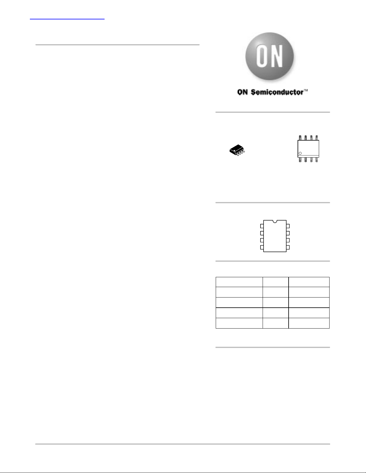
http://onsemi.com
SO–8
8
1
A = Assembly Location
WL, L = Wafer Lot
YY, Y = Year
WW, W = Work Week
D SUFFIX
CASE 751
PIN CONNECTIONS
1
V
GATE
C
OSC
GND
MARKING
DIAGRAM
8
51033
ALYW
1
V
C
CSPGND
V
CC
V
FB
ORDERING INFORMATION*
Device Package Shipping
CS51033YD8 SO–8 95 Units/Rail
CS51033YDR8 2500 Tape & Reel
CS51033GD8
CS51033GDR8 2500 Tape & ReelSO–8
*Additional ordering information can be found on page
9 of this data sheet.
SO–8
SO–8
95 Units/Rail
Semiconductor Components Industries, LLC, 2002
October, 2002 – Rev. 8
1 Publication Order Number:
CS51033/D
Page 2
3.3V
IN
C
100 µF
CS51033
IN
R
10 Ω
C
D
4
1N5818
1N4148
1N4148
V
CC
C
OSC
D
2
D
3
V
C
V
U1
CS51033
GATE
V
FB
C
1
0.1 µF
0.1 µF
R
10 Ω
G
IRF7404
4.7 µH
100
1.5V
OUT
@ 3.0 Amp
C
1.0 µF
2
C
100 µF
C
3
OSC
150 pF
GND
PGND
CS
CS
0.1 µF
0.1 µF
D
1
1N5821
C
100 µF
C
0.1 µF
4
0
100 µF
GND
R
1.5 k
A
R
300
B
Note: Capacitors C2, C3, and C4, are low
ESR tantalum caps used for noise reduction.
Figure 1. Typical Application Diagram
MAXIMUM RATINGS*
Rating Value Unit
Power Supply Voltage, V
Driver Supply Voltage, V
Driver Output Voltage, V
C
, CS, VFB (Logic Pins) 5.0 V
OSC
CC
C
GATE
Peak Output Current 1.0 A
Steady State Output Current 200 mA
Operating Junction Temperature, T
Storage Temperature Range, T
J
S
ESD (Human Body Model) 2.0 kV
Package Thermal Resistance: Junction–to–Case, R
Junction–to–Ambient, R
θ
JC
θ
JA
Lead Temperature Soldering: Reflow (SMD styles only) (Note 1) 230 peak °C
1. 60 sec. max above 183°C.
*The maximum package power dissipation must be observed.
5.0 V
20 V
20 V
150 °C
–65 to 150 °C
45
165
GND
°C/W
°C/W
http://onsemi.com
2
Page 3
CS51033
ELECTRICAL CHARACTERISTICS (Specifications apply for 3.135 ≤ V
Industrial Grade: –40°C < T
Characteristic
< 85°C; –40°C < TJ < 125°C: Commercial Grade: 0°C < TA < 70°C; 0°C < TJ < 125°C, unless otherwise specified.)
A
Test Conditions Min Typ Max Unit
≤ 3.465, 3.0 V ≤ VC ≤ 16 V;
CC
Oscillator VFB = 1.2 V
Frequency C
Charge Current 1.4 V < V
Discharge Current 2.7 V > V
Maximum Duty Cycle 1 – (t
Short Circuit Timer VFB = 1.0 V; CS = 0.1 F; V
= 470 pF 160 200 240 kHz
OSC
< 2.0 V – 110 – µA
COSC
> 2.0 V – 660 – µA
COSC
) 80.0 83.3 – %
OFF/tON
= 2.0 V
COSC
Charge Current 1.0 V < VCS < 2.0 V 175 264 325 µA
Fast Discharge Current 2.55 V > VCS > 2.4 V 40 66 80 µA
Slow Discharge Current 2.4 V > VCS > 1.5 V 4.0 6.0 10 µA
Start Fault Inhibit Time – 0.70 0.85 1.40 ms
Valid Fault Time 2.6 V > VCS > 2.4 V 0.2 0.3 0.45 ms
GATE Inhibit Time 2.4 V > VCS > 1.5 V 9.0 15 23 ms
Duty Cycle – 2.5 3.1 4.6 %
CS Comparator VFB = 1.0 V
Fault Enable CS Voltage – – 2.5 – V
Max. CS Voltage VFB = 1.5 V – 2.6 – V
Fault Detect Voltage VCS when GATE goes high – 2.4 – V
Fault Inhibit Voltage Minimum V
CS
– 1.5 – V
Hold Off Release Voltage VFB = 0 V 0.4 0.7 1.0 V
Regulator Threshold Voltage Clamp VCS = 1.5 V 0.725 0.866 1.035 V
VFB Comparators V
Regulator Threshold Voltage TJ = 25°C (Note 2)
Fault Threshold Voltage TJ = 25°C (Note 2)
= VCS = 2.0 V
COSC
= –40 to 125°C
T
J
T
= –40 to 125°C
J
1.225
1.210
1.12
1.10
1.250
1.250
1.15
1.15
1.275
1.290
1.17
1.19
Threshold Line Regulation 3.135 V ≤ VCC ≤ 3.465 – 6.0 15 mV
Input Bias Current VFB = 0 V – 1.0 4.0 µA
Voltage Tracking (Regulator Threshold – Fault Threshold Voltage) 70 100 120 mV
Input Hysteresis Voltage – – 4.0 20 mV
Power Stage VC = 10 V; VFB = 1.2 V
GATE DC Low Saturation Voltage V
GATE DC High Saturation Voltage V
Rise Time C
Fall Time C
= 1.0 V; 200 mA Sink – 1.2 1.5 V
COSC
= 2.7 V; 200 mA Source; VC = V
COSC
= 1.0 nF; 1.5 V < V
GATE
= 1.0 nF; 9.0 V > V
GATE
GATE
GATE
GATE
< 9.0 V – 25 60 ns
> 1.5 V – 25 60 ns
– 1.5 2.1 V
Current Drain
I
CC
I
C
3.135 V < VCC < 3.465 V, Gate switching – 3.5 6.0 mA
3.0 V < VC < 16 V, Gate non–switching – 2.7 4.0 mA
2. Guaranteed by design, not 100% tested in production.
V
V
V
V
http://onsemi.com
3
Page 4
PACKAGE PIN DESCRIPTION
PIN NUMBER
1 V
2 PGND Output power stage ground connection.
3 C
4 GND Logic ground.
5 V
6 V
7 CS Soft Start and fault timing capacitor.
8 V
C
OSC
V
CC
CS
PIN SYMBOL FUNCTION
GATE
OSC
FB
CC
C
V
CC
I
C
7I
C
V
CC
Driver pin to gate of external PFET.
Oscillator frequency programming capacitor.
Feedback voltage input.
Logic supply voltage.
Driver supply voltage.
Oscillator
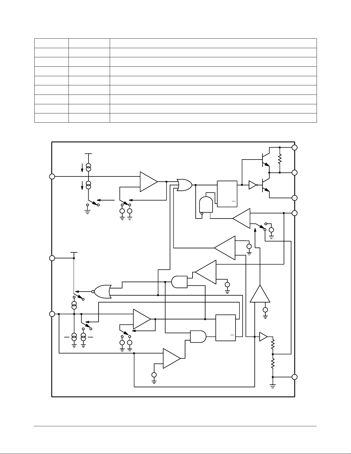
Comparator
+
A1
–
+
–
+
2.5 V1.5 V
–
G3
I
T
CS
Comparator
+
A2
–
55
I
T
I
T
5
+
–
+
2.5 V1.5 V
–
2.4 V
CS51033
G4
–
A3
+
Slow Discharge
+
Comparator
–
G1
G5
G2
Fault
Comp
V
GATE
Flip–Flop
Q
R
F2
Q
S
+
Hold Off
Comp
–
–
1.15 V
+
+
–
Q
R
F1
Q
S
Slow Discharge
Flip–Flop
A6
0.7 V
+
–
V
FB
Comparator
–
1.25 V
+
A4
+
+
–
RG
+
–
CS Charge
Sense
Comparator
–
2.3 V
V
C
V
GATE
PGND
V
FB
GND
Figure 2. Block Diagram
http://onsemi.com
4
Page 5
CS51033
CIRCUIT DESCRIPTION
THEORY OF OPERATION
Control Scheme
The CS51033 monitors the output voltage to determine
when to turn on the PFET. If VFB falls below the internal
reference voltage of 1.25 V during the oscillator’s charge
cycle, the PFET is turned on and remains on for the duration
of the charge time. The PFET gets turned off and remains off
during the oscillator’s discharge cycle time with the
maximum duty cycle to 80%. It requires 7.0 mV typical, and
20 mV maximum ripple on the V
pin to operate. This
FB
method of control does not require any loop stability
compensation.
Startup
The CS51033 has an externally programmable Soft Start
feature that allows the output voltage to come up slowly,
preventing voltage overshoot on the output.
At startup, the voltage on all pins is zero. As V
rises, the
CC
VC voltage along with the internal resistor RG keeps the
PFET off. As VCC and VC continue to rise, the oscillator
capacitor (C
(CS) charges via internal current sources. C
) and the Soft Start/Fault Timing capacitor
OSC
gets charged
OSC
by the current source IC and CS gets charged by the IT source
combination described by:
ICS I
T
55
5
I
I
T
T
The internal Holdoff Comparator ensures that the external
PFET is o f f until VCS > 0.7 V, preventing the GATE flip–flop
(F2) from being set. This allows the oscillator to reach its
operating frequency before enabling the drive output. Soft
Start is obtained by clamping the V
comparator’s (A6)
FB
reference input to approximately 1/2 of the voltage at the CS
pin during startup, permitting the control loop and the output
voltage to slowly increase. Once the CS pin charges above
the Holdoff Comparator trip point of 0.7 V, the low feedback
to the V
C
OSC
V
GATE
2.4 V, the CS charge sense comparator (A4) sets the V
Comparator sets the GATE flip–flop during
FB
’s charge cycle. Once the GATE flip–flop is set,
goes low and turns on the PFET . When VCS exceeds
FB
comparator reference to 1.25 V completing the startup cycle.
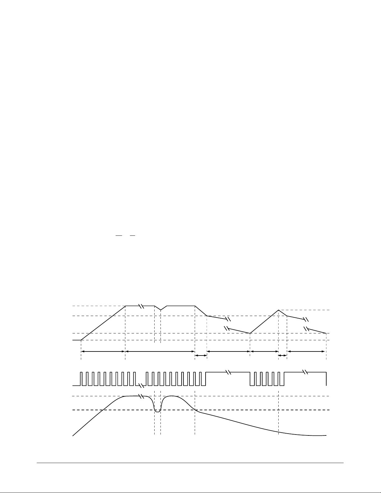
Lossless Short Circuit Protection
The CS51033 has “lossless” short circuit protection since
there is no current sense resistor required. When the voltage
at the CS pin (the fault timing capacitor voltage ) reaches
2.5 V, the fault timing circuitry is enabled. During normal
operation the CS voltage is 2.6 V. During a short circuit or
a transient condition, the output voltage moves lower and the
voltage at VFB drops. If VFB drops below 1.15 V, the output
of the fault comparator goes high and the CS51033 goes into
a fast discharge mode. The fault timing capacitor, CS,
discharges to 2.4 V. If the V
voltage is still below 1.15 V
FB
when the CS pin reaches 2.4 V, a valid fault condition has
been detected. The slow discharge comparator output goes
high and enables gate G5 which sets the slow discharge flip
flop. The V
flip flop resets and the output switch is
GATE
turned off. The fault timing capacitor is slowly discharged
to 1.5 V. The CS51033 then enters a normal startup routine.
If the fault is still present when the fault timing capacitor
voltage reaches 2.5 V, the fast and slow discharge cycles
repeat as shown in Figure 3.
If the V
voltage is above 1 .15 V w hen CS r eaches 2 .4 V
FB
a fault condition is not detected, normal operation resumes
and CS charges back to 2.6 V. This reduces the chance of
erroneously detecting a load transient as a fault condition.
V
V
CS
GATE
V
FB
2.6 V
2.4 V
1.5 V
0 V
1.25 V
1.15 V
S2 S1
S1
START
START NORMAL OPERATION
Figure 3. Voltage on Start Capacitor (VGS), the Gate (V
Feedback Loop (VFB), During Startup, Normal and Fault Conditions.
http://onsemi.com
S2
S3
td1T
5
t
FAULT
S3
FAULT
GATE
S1
t
RESTART
), and in the
S2
S3
td2 t
2.5 V
S3
0 V
FAULT
Page 6

CS51033
Buck Regulator Operation
A block diagram of a typical buck regulator is shown in
Figure 4. If we assume that the output transistor is initially
off, and the system is in discontinuous operation, the
inductor current I
is zero and the output voltage is at its
L
nominal value. The current drawn by the load is supplied by
the output capacitor CO. When the voltage across CO drops
below the threshold established by the feedback resistors R1
Q
V
IN
C
IN
1
D
Control
Feedback
Figure 4. Buck Regulator Block Diagram.
and R2 and the reference voltage V
, the power transistor
REF
Q1 switches on and current flows through the inductor to the
output. The inductor current rises at a rate determined by
(V
IN
– V
)/Load. The duty cycle (or “on” time) for the
OUT
CS51033 is li m ited to 80%. If output voltage remains higher
than nominal during the entire C
change time, the Q1
OSC
does not turn on, skipping the pulse.
L
R
1
C
1
O
R
2
R
LOAD
Charge Pump Circuit
(Refer to the CS51033 Application Diagram on page 2).
An external charge pump circuit is necessary when the V
input voltage is below 5.0 V to ensure that there is suffifient
gate drive voltage for the external FET. When VIN is applied,
capacitors C1 and C2 will be char ged to a diodes drop below
V
via diodes D2 and D4, respectively. When the PFET
IN
APPLICATIONS INFORMATION
DESIGNING A POWER SUPPLY WITH THE CS51033
Specifications
• V
= 3.3 V ±10% (i.e. 3.63 V max., 2.97 V min.)
IN
• V
• I
= 1.5 V ±2.0%
OUT
= 0.3 A to 3.0 A
OUT
• Output ripple voltage < 33 mV.
• F
= 200 kHz
SW
1) Duty Cycle Estimates
Since the maximum duty cycle D, of the CS51033 is
limited to 80% min., it is best to estimate the duty cycle for
the various input conditions to see that the design will work
over the complete operating range.
The duty cycle for a buck regulator operating in a
continuous conduction mode is given by:
V
V
D
OUT
VIN V
D
SAT
turns on, it’s drain voltage will be approximately equal to
VIN. Since the voltage across C1 can not change
instantaneously, D2 is reverse biased and the anode voltage
C
rises to approximately 2.0 × 3.3 V – VD2. C1 transfers some
of its stored charge C2 via D3. After several cycles there is
sufficient gate drive voltage.
In this case we can assume that VD = 0.6 V and V
0.6 V so the equation reduces to:
V
OUT
D
V
IN
From this, the maximum duty cycle D
MAX
occurs when VIN is a t i t ’s minimum while the minimum duty
cycle D
2) Switching Frequency and On and Off Time
Calculations
is 0.35%.
MIN
FSW = 200 kHz. The switching frequency is determined
by C
, whose value is determined by:
OSC
C
OSC
T
1
1.0
F
F
SW
310
SW
95
F
SW
6
5.0 s
3010
F
SW
3
is 53%, this
470 pF
2
SAT
=
where:
V
SAT
= R
DS(ON)
× I
OUT
Max.
http://onsemi.com
6
Page 7

CS51033
T
ON(MAX)
T
ON(MIN)
T
OFF(MAX)
3) Inductor Selection
5.0 s 0.53 2.65 s
5.0 s 0.35 1.75 s
5.0 s 0.7 s 4.3 s
Pick the inductor value to maintain continuous mode
operation down to 0.3 Amps.
The ripple current ∆I = 2 × I
V
VD T
L
MIN
OUT
OFF(MAX)
I
OUT(MIN)
= 2 × 0.3 A = 0.6 A.
2.1 V 4.3 s
0.6 A
15 H
The CS51033 will operate with almost any value of
inductor. With larger inductors the ripple current is reduced
and the regulator will remain in a continuous conduction
mode for lower values of load current. A smaller inductor
will result in lar ger ripple current. The core must not saturate
with the maximum expected current, here given by:
I
I
OUT
2.0
3.0 A 0.6 A2.0 3.3 A
I
MAX
4) Output Capacitor
The output capacitor limits the output ripple voltage. The
CS51033 needs a maximum of 15 mV of output ripple for
the feedback comparator to change state. If we assume that
all the inductor ripple current flows through the output
capacitor and that it is an ideal capacitor (i.e. zero ESR), the
minimum capacitance needed to limit the output ripple to
50 mV peak to peak is given by:
C
O
8.0 FSW V
8.0 (200 103Hz
I
0.6 A
)(
33 103V
11.4 F
)
The minimum ESR needed to limit the output voltage
ripple to 50 mV peak to peak is:
ESR
V
I
50 10
0.6 A
3
55 m
The output capacitor should be chosen so that its ESR is
at least half of the calculated value and the capacitance is at
least ten times the calculated value. It is often advisable to
use several capacitors in parallel to reduce ESR.
Low impedance aluminum electrolytic, tantalum or
organic semiconductor capacitors are a good choice for an
output capacitor. Low impedance aluminum are the
cheapest but are not available in surface mount at present.
Solid tantalum chip capacitors are available from a number
of suppliers and offer the best choice for surface mount
applications. The capacitor working voltage should be
greater than the output voltage in all cases.
5) VFB Divider
V
OUT
1.25 V
R1 R2
R2
1.25 V
R1
R2
1.0
The input bias current to the comparator is 4.0 µA. The
resistor divider current should be considerably higher than
this to ensure that there is sufficient bias current. If we
choose the divider current to be at least 250 times the bias
current this gives a divider current of 1.0 mA and simplifies
the calculations.
1.5 V
1.0 mA
R1 R2 1.5 k
Let R2 = 1.0 k
Rearranging the divider equation gives:
V
OUT
R1 R2
6) Divider Bypass Capacitor C
1.0 1.0 k
1.25
RR
1.5 V
1.25
200
Since the feedback resistors divide the output voltage by
a factor of 4.0, i.e. 5.0 V/1.25 V= 4.0, it follows that the
output ripple is also divided by four. This would require that
the output ripple be at least 60 mV (4.0 × 15 mV) to trip the
feedback comparator. We use a capacitor C
to act as an
RR
AC short so that the output ripple is not attenuated by the
divider network. The ripple voltage frequency is equal to the
switching frequency so we choose C
1.0
X
C
2fC
so that:
RR
is negligible at the switching frequency.
In this case FSW is 200 kHz if we allow X
1.0
C
7) Soft Start and Fault Timing Capacitor CS
2f3
0.265 F
= 3.0 Ω then:
C
CS performs several important functions. First it provides
a dead time for load transients so that the IC does not enter
a fault mode every time the load changes abruptly. Secondly
it disables the fault circuitry during startup, it also provides
Soft Start by clamping the reference voltage during startup
to rise slowly and finally it controls the hiccup short circuit
protection circuitry. This function reduces the PFET’s duty
cycle to 2.0% of the CS period.
The most important consideration in calculating CS is that
it’s voltage does not reach 2.5 V (the voltage at which the
fault detect circuitry is enabled) before V
reaches 1.15 V
FB
otherwise the power supply will never start.
If the VFB pin reaches 1.15 V, the fault timing comparator
will discharge CS and the supply will not start. For the V
FB
voltage to reach 1.15 V the output voltage must be at least
4 × 1.15 = 4.6 V.
http://onsemi.com
7
Page 8

CS51033
If we choose an arbitrary startup time of 200 µs, we
calculate the value of CS from:
CS 2.5 V
T
I
CHARGE
CS
(MIN)
200 s 264 A
2.5 V
0.02 F
Use 0.1 µF.
The fault time out time is the sum of the slow discharge
time the fast discharge time and the recharge time and is
obviously dominated by the slow discharge time.
The first parameter is the slow discharge time, it is the time
for the CS capacitor to discharge from 2.4 V to 1.5 V and is
given by:
T
SLOWDISCHARGE
where I
DISCHARGE
T
SLOWDISCHARGE
CS (2.4 V 1.5 V
I
is 6.0 µA typical.
CS 1.5 V 10
DISCHARGE
)
5
The fast discharge time occurs when a fault is first
detected. The C S ca pa citor i s d ischarged from 2.5 V to 2 .4 V.
)
where I
T
FASTDISCHARGE
FASTDISCHARGE
T
FASTDISCHARGE
CS (2.5 V 2.4 V
I
FASTDISCHARGE
is 66 µA typical.
CS 1515
The recharge time is the time for CS to charge from 1.5 V
to 2.5 V.
)
where I
T
CHARGE
CHARGE
CS (2.5 V 1.5 V
I
CHARGE
is 264 µA typical.
T
CHARGE
CS 3787
The fault time out time is given by:
5
T
FAULT
CS (3787 1515 1.5 10
T
FAULT
CS (1.55 10
5
)
)
For this circuit
T
FAULT
0.1 106 1.55 105 0.0155
A larger value of CS will increase the fault time out time
but will also increase the Soft Start time.
8) Input Capacitor
The input capacitor reduces the peak currents drawn from
the input supply and reduces the noise and ripple voltage on
the VCC and VC pins. This capacitor must also ensure that
the V
remains above the UVLO voltage in the event of an
CC
output short circuit. CIN should be a low ESR capacitor of
at least 100 µF. A ceramic surface mount capacitor should
also be connected between VCC and ground to prevent
spikes.
9) MOSFET Selection
The CS51033 drives a P–channel MOSFET. The V
GATE
pin swings from GND to VC. The type of PFET used
depends on the operating conditions but for input voltages
below 7.0 V a logic level FET should be used.
Choose a PFET with a continuous drain current (I
greater than the maximum output current. R
DS(ON)
) rating
D
should
be less than
R
DS
0.6 V
I
OUT(MAX)
167 m
The Gate–to–Source voltage VGS and the Drain–to
Source Breakdown Voltage should be chosen based on the
input supply voltage.
The power dissipation due to the conduction losses is
given by:
OUT
2
R
DS(ON)
D
PD I
The power dissipation due to the switching losses is given
by:
r
PD 0.5 VIN I
OUT
(
T
R
where TR = Rise Time and TF = Fall Time
10) Diode Selection
T
)
F
F
SW
.
The flyback or catch diode should be a Schottky diode
because of i t ’s fast switching ability and low forward voltage
drop. The current rating must be at least equal to the
maximum output current. The breakdown voltage should be
at least 20 V for this 12 V application.
The diode power dissipation is given by:
PD I
OUT
V
D
(
1.0 D
MIN
)
http://onsemi.com
8
Page 9

CS51033YD8
CS51033YDR8
CS51033GD8
CS51033GDR8
Device
CS51033
ORDERING INFORMATION
Operating
Temperature Range
–40°C < TA < 85°C
0°C < TA < 70°C
Package Shipping
95 Units/Rail
SO–8
2500 Tape & Reel
95 Units/Rail
2500 Tape & Reel
http://onsemi.com
9
Page 10

–Y–
–Z–
CS51033
PACKAGE DIMENSIONS
SO–8
D SUFFIX
CASE 751–07
ISSUE AA
NOTES:
–X–
A
58
B
1
S
0.25 (0.010)
4
M
M
Y
K
G
C
SEATING
PLANE
0.10 (0.004)
H
D
0.25 (0.010) Z
M
Y
SXS
N
X 45
M
1. DIMENSIONING AND TOLERANCING PER ANSI
Y14.5M, 1982.
2. CONTROLLING DIMENSION: MILLIMETER.
3. DIMENSION A AND B DO NOT INCLUDE MOLD
PROTRUSION.
4. MAXIMUM MOLD PROTRUSION 0.15 (0.006) PER
SIDE.
5. DIMENSION D DOES NOT INCLUDE DAMBAR
PROTRUSION. ALLOWABLE DAMBAR
PROTRUSION SHALL BE 0.127 (0.005) TOTAL IN
EXCESS OF THE D DIMENSION AT MAXIMUM
MATERIAL CONDITION.
6. 751-01 THRU 751-06 ARE OBSOLETE. NEW
STANDAARD IS 751-07
MILLIMETERS
DIMAMIN MAX MIN MAX
4.80 5.00 0.189 0.197
B 3.80 4.00 0.150 0.157
C 1.35 1.75 0.053 0.069
D 0.33 0.51 0.013 0.020
G 1.27 BSC 0.050 BSC
H 0.10 0.25 0.004 0.010
J
J 0.19 0.25 0.007 0.010
K 0.40 1.27 0.016 0.050
M 0 8 0 8
N 0.25 0.50 0.010 0.020
S 5.80 6.20 0.228 0.244
INCHES
http://onsemi.com
10
Page 11

Notes
CS51033
http://onsemi.com
11
Page 12

CS51033
ON Semiconductor and are registered trademarks of Semiconductor Components Industries, LLC (SCILLC). SCILLC reserves the right to make
changes without further notice to any products herein. SCILLC makes no warranty, representation or guarantee regarding the suitability of its products for any
particular purpose, nor does SCILLC assume any liability arising out of the application or use of any product or circuit, and specifically disclaims any and all
liability, including without limitation special, consequential or incidental damages. “Typical” parameters which may be provided in SCILLC data sheets and/or
specifications can and do vary in different applications and actual performance may vary over time. All operating parameters, including “Typicals” must be
validated for each customer application by customer’s technical experts. SCILLC does not convey any license under its patent rights nor the rights of others.
SCILLC products are not designed, intended, or authorized for use as components in systems intended for surgical implant into the body, or other applications
intended to support or sustain life, or for any other application in which the failure of the SCILLC product could create a situation where personal injury or death
may occur. Should Buyer purchase or use SCILLC products for any such unintended or unauthorized application, Buyer shall indemnify and hold SCILLC
and its officers, employees, subsidiaries, affiliates, and distributors harmless against all claims, costs, damages, and expenses, and reasonable attorney fees
arising out of, directly or indirectly, any claim of personal injury or death associated with such unintended or unauthorized use, even if such claim alleges that
SCILLC was negligent regarding the design or manufacture of the part. SCILLC is an Equal Opportunity/Affirmative Action Employer.
PUBLICATION ORDERING INFORMATION
Literature Fulfillment:
Literature Distribution Center for ON Semiconductor
P.O. Box 5163, Denver, Colorado 80217 USA
Phone: 303–675–2175 or 800–344–3860 Toll Free USA/Canada
Fax: 303–675–2176 or 800–344–3867 Toll Free USA/Canada
Email: ONlit@hibbertco.com
N. American Technical Support: 800–282–9855 Toll Free USA/Canada
http://onsemi.com
JAPAN: ON Semiconductor, Japan Customer Focus Center
2–9–1 Kamimeguro, Meguro–ku, Tokyo, Japan 153–0051
Phone: 81–3–5773–3850
Email: r14525@onsemi.com
ON Semiconductor Website: http://onsemi.com
For additional information, please contact your local
Sales Representative.
CS51033/D
12
 Loading...