

Page 1
CM6305
EMI Filter with ESD
Protection for SIM Card
Applications
Product Description
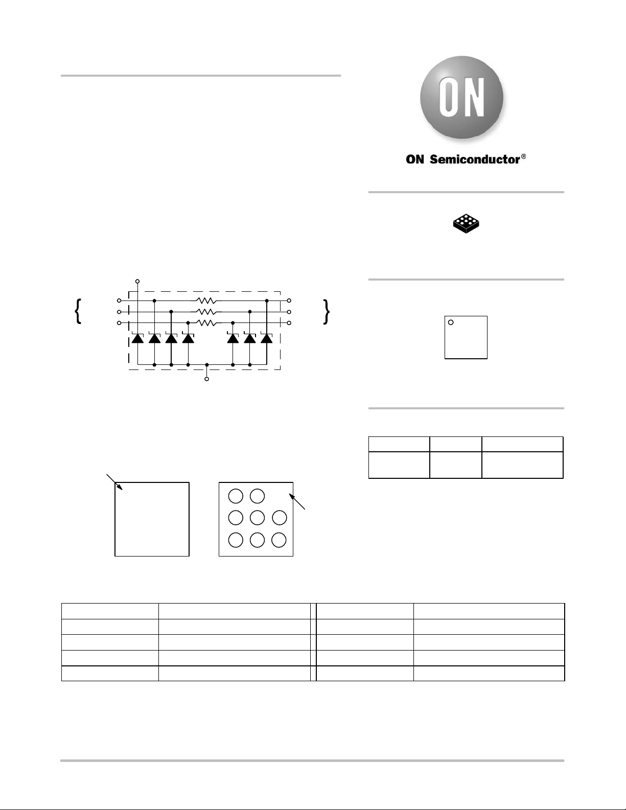
The CM6305 is a 3 x 3, 8−bump EMI filter with ESD protection
device for SIM card applications in a 0.4 mm pitch CSP form factor. It
is fully compliant with IEC 61000−4−2. The CM6305 is also RoHS II
compliant.
ELECTRICAL SCHEMATIC
V (C2) {External}
GND (B2)
A
B
C
R1
R2
R3
Bottom View
(Bumps Up View)
23
A2A3
B2B3
C1C2C3
1
B1
I1 (A2)
I2 (B1)
I3 (C1)
A1
A1 Corner
Indicator
O1 (A3)
O2 (B3)
O3 (C3)
Internal
Orientation
Marking
PACKAGE / PINOUT DIAGRAMS
Top View
(Bumps Down View)
123
+
A
B
C
65
External
http://onsemi.com
WLCSP8
CASE 567CE
MARKING DIAGRAM
65
YWW
65 = CM6305
YWW = Date Code
ORDERING INFORMATION
Device Package Shipping
WLCSP−8
(Pb−Free)
†For information on tape and reel specifications,
including part orientation and tape sizes, please
refer to our Tape and Reel Packaging Specification
Brochure, BRD8011/D.
5000/Tape & ReelCM6305
†
Table 1. PIN DESCRIPTIONS
Pin Description Pin Description
A2 Channel 1 External A3 Channel 1 Internal
B1 Channel 2 External B3 Channel 2 Internal
C1 Channel 3 External C3 Channel 3 Internal
B2 GND C2 V External
© Semiconductor Components Industries, LLC, 2011
August, 2011 − Rev. 2
1 Publication Order Number:
CM6305/D
Page 2
CM6305
ELECTRICAL SPECIFICATIONS AND CONDITIONS
Table 2. PARAMETERS AND OPERATING CONDITIONS
Parameter Rating Units
Storage Temperature Range –55 to +150 °C
Operating Temperature Range –40 to +85 °C
Power Dissipation at 70°C per Channel 60 mW
Table 3. ELECTRICAL OPERATING CHARACTERISTICS (Note 1)
Symbol Parameter Conditions Min Typ Max Units
R
Resistance 80 100 120
1
R
Resistance 37.6 47 56.4
2
R
Resistance 80 100 120
3
I
LEAK
V
1. All parameters specified at TA = 25°C unless otherwise noted.
2. Standard IEC 61000−4−2 with C
Leakage Current per Channel VIN = 3.0 V 10 100 nA
C
Capacitance on Filter Channels 1, 2 and 3 At 1 MHz, V
Capacitance on Clamp Channel (pin C2) At 1 MHz, V
V
Breakdown Voltage (Positive) I
B
ESD Protection Peak Discharge Voltage at A2, B1 and C1 pins
ESD
a) Contact Discharge per IEC 61000−4−2 standard
b) Air Discharge per IEC 61000−4−2 standard
ESD Protection Peak Discharge Voltage at C2 pin
a) Contact Discharge per IEC 61000−4−2 standard
b) Air Discharge per IEC 61000−4−2 standard
ESD Protection Peak Discharge Voltage at A3, B3 and C3 pins
a) Contact Discharge per IEC 61000−4−2 standard
b) Air Discharge per IEC 61000−4−2 standard
Discharge
= 150 pF, R
Discharge
= 330 W.
= 1 mA 6 7 9 V
R
(Note 2)
(Note 2)
(Note 2)
= 0 V 8 10 12 pF
IN
= 0 V 8 10 12 pF
IN
±8
±15
±15
±15
±2
±2
W
W
W
kV
kV
kV
Table 4. CSP TAPE AND REEL SPECIFICATIONS
Pocket Size (mm)
Part Number Chip Size (mm)
†
B0 X A0 X K
Tape Width
0
W
Reel Dia. Qty Per Reel P
P
0
1
CM6305 1.16 X 1.16 X 0.60 1.27 X 1.27 X 0.69 8 mm 178 mm (7″) 5000 4 mm 4 mm
†For information on tape and reel specifications, including part orientation and tape sizes, please refer to our Tape and Reel Packaging
Specification Brochure, BRD8011/D.
http://onsemi.com
2
Page 3

CM6305
RF CHARACTERISTICS
Figure 1. Insertion Loss, Filter 1 (pins A2, A3) and Filter 3 (pins C1, C3) (Bias = 0 V, TA = 255C)
Figure 2. Insertion Loss, Filter 2 (pins B1, B3) (Bias = 0 V, TA = 255C)
http://onsemi.com
3
Page 4

MECHANICAL CASE OUTLINE
PACKAGE DIMENSIONS
SCALE 4:1
WLCSP8, 1.16x1.16
CASE 567CE−01
ISSUE O
DATE 27 JUL 2010
REFERENCE
2X
2X
NOTE 3
0.03
PIN A1
0.05 C
8X
A0.05 BC
C
0.05 C
0.05 C
0.05 C
A1
b
D
TOP VIEW
SIDE VIEW
C
B
A
12 3
BOTTOM VIEW
A
B
E
A2
A
SEATING
C
PLANE
e
e
NOTES:
1. DIMENSIONING AND TOLERANCING PER
ASME Y14.5M, 1994.
2. CONTROLLING DIMENSION: MILLIMETERS.
3. COPLANARITY APPLIES TO SPHERICAL
CROWNS OF SOLDER BALLS.
MILLIMETERS
DIMAMIN MAX
0.57
A1
0.17 0.24
A2 0.41 REF
b 0.24 0.29
D 1.16 BSC
E
1.16 BSC
e 0.40 BSC
RECOMMENDED
SOLDERING FOOTPRINT*
A1
0.40
PITCH
DIMENSIONS: MILLIMETERS
0.63
PACKAGE
OUTLINE
8X
0.40
PITCH
0.25
*For additional information on our Pb−Free strategy and soldering
details, please download the ON Semiconductor Soldering and
Mounting Techniques Reference Manual, SOLDERRM/D.
DOCUMENT NUMBER:
DESCRIPTION:
ON Semiconductor and are trademarks of Semiconductor Components Industries, LLC dba ON Semiconductor or its subsidiaries in the United States and/or other countries.
ON Semiconductor reserves the right to make changes without further notice to any products herein. ON Semiconductor makes no warranty, representation or guarantee regarding
the suitability of its products for any particular purpose, nor does ON Semiconductor assume any liability arising out of the application or use of any product or circuit, and specifically
disclaims any and all liability, including without limitation special, consequential or incidental damages. ON Semiconductor does not convey any license under its patent rights nor the
rights of others.
© Semiconductor Components Industries, LLC, 2019
98AON50308E
WLCSP8, 1.16X1.16
Electronic versions are uncontrolled except when accessed directly from the Document Repository.
Printed versions are uncontrolled except when stamped “CONTROLLED COPY” in red.
PAGE 1 OF 1
www.onsemi.com
Page 5

ON Semiconductor and are trademarks of Semiconductor Components Industries, LLC dba ON Semiconductor or its subsidiaries in the United States and/or other countries.
ON Semiconductor owns the rights to a number of patents, trademarks, copyrights, trade secrets, and other intellectual property. A listing of ON Semiconductor’s product/patent
coverage may be accessed at www.onsemi.com/site/pdf/Patent−Marking.pdf
ON Semiconductor makes no warranty, representation or guarantee regarding the suitability of its products for any particular purpose, nor does ON Semiconductor assume any liability
arising out of the application or use of any product or circuit, and specifically disclaims any and all liability, including without limitation special, consequential or incidental damages.
Buyer is responsible for its products and applications using ON Semiconductor products, including compliance with all laws, regulations and safety requirements or standards,
regardless of any support or applications information provided by ON Semiconductor. “Typical” parameters which may be provided in ON Semiconductor data sheets and/or
specifications can and do vary in different applications and actual performance may vary over time. All operating parameters, including “Typicals” must be validated for each customer
application by customer’s technical experts. ON Semiconductor does not convey any license under its patent rights nor the rights of others. ON Semiconductor products are not
designed, intended, or authorized for use as a critical component in life support systems or any FDA Class 3 medical devices or medical devices with a same or similar classification
in a foreign jurisdiction or any devices intended for implantation in the human body. Should Buyer purchase or use ON Semiconductor products for any such unintended or unauthorized
application, Buyer shall indemnify and hold ON Semiconductor and its officers, employees, subsidiaries, affiliates, and distributors harmless against all claims, costs, damages, and
expenses, and reasonable attorney fees arising out of, directly or indirectly, any claim of personal injury or death associated with such unintended or unauthorized use, even if such
claim alleges that ON Semiconductor was negligent regarding the design or manufacture of the part. ON Semiconductor is an Equal Opportunity/Affirmative Action Employer. This
literature is subject to all applicable copyright laws and is not for resale in any manner.
. ON Semiconductor reserves the right to make changes without further notice to any products herein.
PUBLICATION ORDERING INFORMATION
LITERATURE FULFILLMENT:
Email Requests to: orderlit@onsemi.com
ON Semiconductor Website: www.onsemi.com
TECHNICAL SUPPORT
North American Technical Support:
Voice Mail: 1 800−282−9855 Toll Free USA/Canada
Phone: 011 421 33 790 2910
Europe, Middle East and Africa Technical Support:
Phone: 00421 33 790 2910
For additional information, please contact your local Sales Representative
◊
www.onsemi.com
1
 Loading...