

Page 1
CM1451
LCD and Camera EMI Filter
Array with ESD Protection
Description
The CM1451 is an inductor−capacitor (L−C) based EMI filter array
with integrated ESD protection in CSP. The CM1451−06 and
CM1451−08 are configured in 6 and 8 channel formats respectively.
Each channel is implemented as a 5−pole L−C filter with the
component values 9.5 pF − 17 nH − 9.5 pF − 17 nF − 9.5 pF. The
CM1451’s roll−off frequency at −10 dB attenuation is 500 MHz. It can
be used in applications where the data rates are as high as 200 Mbps
while providing greater than 35 dB attenuation over the 800 MHz to
2.7 GHz frequency range. The device has ESD protection diodes on
every pin that provide a very high level of protection for sensitive
electronic components that may be subjected to electrostatic discharge
(ESD). The ESD protection diodes connected to the filter ports safely
dissipate ESD strikes of ±15 kV, exceeding the Level 4 requirement of
the IEC61000−4−2 international standard. Using the MIL−STD−883
(Method 3015) specification for Human Body Model (HBM) ESD, the
pins are protected for contact discharges at greater than ±30 kV.
This device is particularly well−suited for portable electronics (e.g.
wireless handsets, PDAs) because of its small package format and
easy−to−use pin assignments. In particular, the CM1451 is ideal for
EMI filtering and protecting data and control lines for the LCD display
and camera interface in wireless handsets while maintaining the
integrity of signals that have rise/fall times as fast as 2 ns.
The CM1451 incorporates OptiGuard, a coating that results in
improved reliability at assembly. The CM1451 is available in a
space−saving, low−profile Chip Scale Package with RoHS compliant
lead−free finishing.
Features
• High Bandwidth, High RF Rejection Filter Array
• Six and Eight Channels of EMI Filtering
• Utilizes Inductor−Based Design Technology for True L−C Filter
Implementation
• OptiGuard Coating for Improved Reliability
• Chip Scale Package (CSP) Features Extremely Low Lead
Inductance for Optimum Filter and ESD Performance
• 15 kV ESD Protection on Each Channel
(IEC 61000−4−2 Level 4, Contact Discharge)
• 30 kV ESD Protection on Each Channel (HBM)
• Better than 40 dB of Attenuation at 1 GHz
• Maintains Signal Integrity for Signals that Have a
Risetime and Falltime as Fast as 2 ns
• 15−Bump, 3.006 mm x 1.376 mm Footprint Chip Scale
Package (CM1451−06CP)
• 20−Bump, 4.006 mm x 1.376 mm Footprint Chip Scale
Package (CM1451−08CP)
• These Devices are Pb−Free and are RoHS Compliant
http://onsemi.com
WLCSP15
CP SUFFIX
CASE 567BT
MARKING DIAGRAM
N516
CM1451−06
15−Bump CSP Package
N516 = CM1451−06CP
N518 = CM1451−08CP
ORDERING INFORMATION
Device Package Shipping
CM1451−06CP CSP−15
(Pb−Free)
CM1451−08CP CSP−20
(Pb−Free)
†For information on tape and reel specifications,
including part orientation and tape sizes, please
refer to our Tape and Reel Packaging Specification
Brochure, BRD8011/D.
WLCSP20
CP SUFFIX
CASE 567CL
N518
CM1451−08
20−Bump CSP Package
†
3500/Tape & Reel
3500/Tape & Reel
Applications
• LCD and Camera Data Lines in Mobile Handsets
• I/O Port Protection for Mobile Handsets, Notebook
Computers, PDAs, etc.
• Wireless Handsets / Cell Phones
© Semiconductor Components Industries, LLC, 2013
April, 2013 − Rev. 3
• EMI Filtering for Data Ports in Cell Phones, PDAs or
Notebook Computers
• Handheld PCs / PDAs
• LCD and Camera Modules
1 Publication Order Number:
CM1451/D
Page 2
CM1451
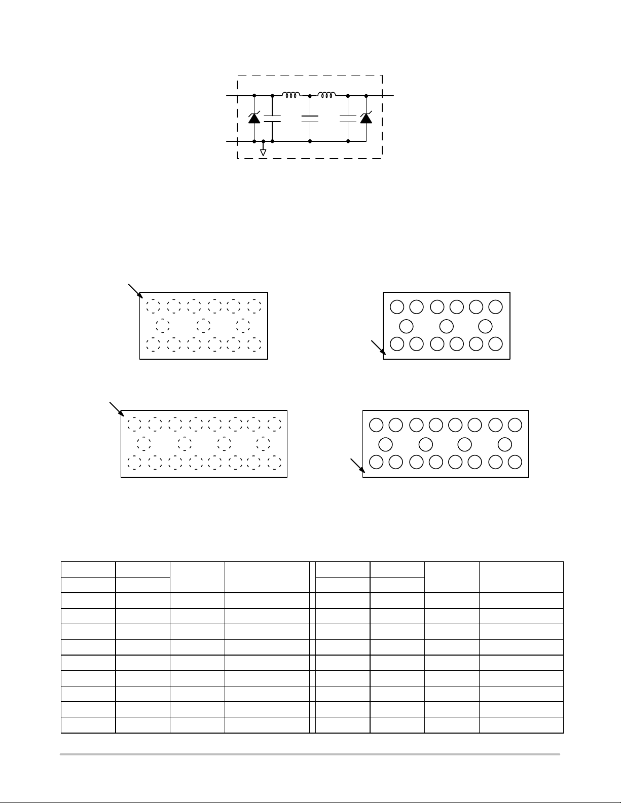
BLOCK DIAGRAM
Orientation
Marking
(see Note)
Orientation
Marking
(see Note)
A
B
C
123
+
A
L1
FILTERn*
C1
GND
(Pins B1−Bm)
1 of n EMI Filtering + ESD Channels
(n = 6 for CM1451−06, 8 for CM1451−08, m=n/2)
*See Package/Pinout Diagrams for expanded pin information.
L2
C2 C3
PACKAGE / PINOUT DIAGRAMS
Top View
(Bumps Down View)
123
564
+
N516
CM1451−06CP
15−Bump CSP Package
56748
Orientation
Marking
C1 C2
A1 A2
A1
C1 C2
FILTERn*
Bottom View
(Bumps Up View)
C3 C4
B1
A3 A4
C3 C4
B2
C5 C6
C5 C6
B3
A5 A6
C7 C8
B
C
Note: Lead−free devices are specified by using a “+” character for the top side orientation mark.
N518
Orientation
Marking
CM1451−08CP
20−Bump CSP Package
B1
A1 A2
A1
B2
A3 A4
B3
A5 A6
A7 A8
Table 1. PIN DESCRIPTIONS
CM1451−06 CM1451−08
Pin(s) Pin(s) Pin(s) Pin(s)
A1 A1 FILTER1 Filter Channel 1 C1 C1 FILTER1 Filter Channel 1
A2 A2 FILTER2 Filter Channel 2 C2 C2 FILTER2 Filter Channel 2
A3 A3 FILTER3 Filter Channel 3 C3 C3 FILTER3 Filter Channel 3
A4 A4 FILTER4 Filter Channel 4 C4 C4 FILTER4 Filter Channel 4
A5 A5 FILTER5 Filter Channel 5 C5 C5 FILTER5 Filter Channel 5
A6 A6 FILTER6 Filter Channel 6 C6 C6 FILTER6 Filter Channel 6
− A7 FILTER7 Filter Channel 7 − C7 FILTER7 Filter Channel 7
− A8 FILTER8 Filter Channel 8 − C8 FILTER8 Filter Channel 8
B1−B3 B1−B4 GND Device Ground
Name Description
CM1451−06 CM1451−08
Name Description
B4
http://onsemi.com
2
Page 3
CM1451
SPECIFICATIONS
Table 2. ABSOLUTE MAXIMUM RATINGS
Parameter Rating Units
Storage Temperature Range −65 to +150 °C
Current per Inductor 30 mA
DC Package Power Rating 500 mW
Stresses exceeding Maximum Ratings may damage the device. Maximum Ratings are stress ratings only. Functional operation above the
Recommended Operating Conditions is not implied. Extended exposure to stresses above the Recommended Operating Conditions may affect
device reliability.
Table 3. STANDARD OPERATING CONDITIONS
Parameter Rating Units
Operating Temperature Range −40 to +85 °C
Table 4. ELECTRICAL OPERATING CHARACTERISTICS (Note 1)
Symbol
L
TOT
L1, L
R
DC IN−OUT
C
TOT
Total Channel Inductance (L1 + L2) 34 nH
Inductance 17 nH
2
DC Channel Resistance 18
Total Channel Capacitance (C1 + C2 + C3) At 2.5 V DC, 1 MHz,
C1, C2, C3Capacitance At 2.5 V DC, 1 MHz,
f
V
DIODE
I
LEAK
V
f
RO
SIG
C
Cut−off Frequency
SOURCE
= 50 W, Z
Z
Roll−off Frequency at −10 dB Attenuation
SOURCE
= 50 W, Z
Z
Diode Standoff Voltage
Diode Leakage Current V
Signal Clamp Voltage
Positive Clamp
Negative Clamp
V
ESD
In−system ESD Withstand Voltage
a) Human Body Model, MIL−STD−883, Method 3015
b) Contact Discharge per IEC 61000−4−2 Level 4
R
DYN
Dynamic Resistance
Positive
Negative
1. T
= 25°C unless otherwise specified.
A
2. ESD applied to input and output pins with respect to GND, one at a time.
Parameter Conditions Min Typ Max Units
W
22.8 28.5 34.2 pF
30 mV AC
7.6 9.5 11.4 pF
30 mV AC
MHz
LOAD
= 50 W
260
MHz
5.6
500
6.0 V
6.8
−0.8
9.0
−0.4
mA
V
kV
LOAD
= 50 W
I
= 10 mA
DIODE
= +3.3 V 0.1 1.0
DIODE
I
= 10 mA
LOAD
−1.5
(Note 2)
30
15
W
2.30
0.90
http://onsemi.com
3
Page 4
CM1451
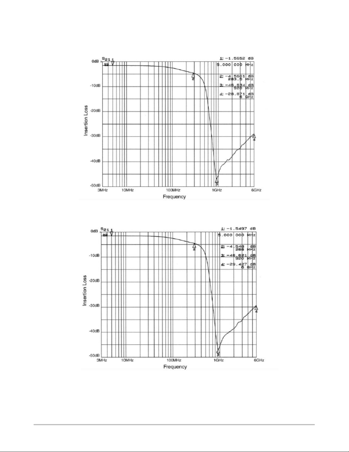
PERFORMANCE INFORMATION
Typical Filter Performance (TA = 255C, DC Bias = 0 V, 50 W Environment)
Figure 1. Insertion Loss vs. Frequency (A1−C1 to GND B1)
Figure 2. Insertion Loss vs. Frequency (A2−C2 to GND B1)
http://onsemi.com
4
Page 5

CM1451
PERFORMANCE INFORMATION (Cont’d)
Typical Filter Performance (TA = 255C, DC Bias = 0 V, 50 W Environment)
Figure 3. Insertion Loss vs. Frequency (A3−C3 to GND B2)
Figure 4. Insertion Loss vs. Frequency (A4−C4 to GND B2)
http://onsemi.com
5
Page 6

CM1451
PERFORMANCE INFORMATION (Cont’d)
Typical Filter Performance (TA = 255C, DC Bias = 0 V, 50 W Environment)
Figure 5. Insertion Loss vs. Frequency (A5−C5 to GND B3)
Figure 6. Insertion Loss vs. Frequency (A6−C6 to GND B3)
http://onsemi.com
6
Page 7

CM1451
PERFORMANCE INFORMATION (Cont’d)
[pF]
D. C.Vo ltag e
Figure 7. Filter Capacitance vs. Input Voltage over Temperature
(normalized to capacitance at 2.5 VDC and 255C)
Transient Response Characteristics
Figure 8. Simulated Transient Response
(input signal risetime and falltime = 2 ns, clocked at 25, 50 and 75 MHz,
15 W Source Resistance, 5 pF Load)
http://onsemi.com
7
Page 8

CM1451
APPLICATION INFORMATION
Table 5. PRINTED CIRCUIT BOARD RECOMMENDATIONS
Parameter Value
Pad Size on PCB 0.240 mm
Pad Shape Round
Pad Definition Non−Solder Mask defined pads
Solder Mask Opening 0.290 mm Round
Solder Stencil Thickness 0.125 − 0.150 mm
Solder Stencil Aperture Opening (laser cut, 5% tapered walls) 0.300 mm Round
Solder Flux Ratio 50/50 by volume
Solder Paste Type No Clean
Pad Protective Finish OSP (Entek Cu Plus 106A)
Tolerance − Edge To Corner Ball
Solder Ball Side Coplanarity
Maximum Dwell Time Above Liquidous 60 seconds
Maximum Soldering Temperature for Lead−free Devices using a Lead−free Solder Paste 260°C
±50 mm
±20 mm
Non−Solder Mask Defined Pad
0.240 mm DIA.
Solder Stencil Opening
0.300 mm DIA.
Solder Mask Opening
0.290 mm DIA.
Figure 9. Recommended Non−Solder Mask Defined Pad Illustration
250
200
150
100
Temperature (5C)
50
0 1:00.0 2:00.0 3:00.0 4:00.0
Time (minutes)
Figure 10. Lead−free (SnAgCu) Solder Ball Reflow Profile
http://onsemi.com
8
Page 9

MECHANICAL CASE OUTLINE
PACKAGE DIMENSIONS
SCALE 4:1
D
PIN A1
REFERENCE
2X
0.05 C
2X
0.05 C
0.05 C
TOP VIEW
OptiGuard Option
WLCSP15, 3.01x1.38
CASE 567BT−01
ISSUE O
A
B
E
A2
DATE 26 JUL 2010
NOTES:
1. DIMENSIONING AND TOLERANCING PER
ASME Y14.5M, 1994.
2. CONTROLLING DIMENSION: MILLIMETERS.
3. COPLANARITY APPLIES TO SPHERICAL
CROWNS OF SOLDER BALLS.
MILLIMETERS
DIMAMIN MAX
A1
A2 0.42 REF
b 0.29 0.35
D 3.01 BSC
E
eD 0.50 BSC
eE 0.435 BSC
0.72
0.56
0.21 0.27
1.38 BSC
NOTE 3
0.03 C
0.05 C
15X
A0.05 BC
A1
b
SIDE VIEW
C
B
A
123 789
456
BOTTOM VIEW
eD/2
eD
A
RECOMMENDED
SOLDERING FOOTPRINT*
PACKAGE
OUTLINE
15X
0.25
eE
C
SEATING
PLANE
A1
0.87
0.44
0.50
PITCH
DIMENSIONS: MILLIMETERS
*For additional information on our Pb−Free strategy and soldering
details, please download the ON Semiconductor Soldering and
Mounting Techniques Reference Manual, SOLDERRM/D.
DOCUMENT NUMBER:
DESCRIPTION:
ON Semiconductor and are trademarks of Semiconductor Components Industries, LLC dba ON Semiconductor or its subsidiaries in the United States and/or other countries.
ON Semiconductor reserves the right to make changes without further notice to any products herein. ON Semiconductor makes no warranty, representation or guarantee regarding
the suitability of its products for any particular purpose, nor does ON Semiconductor assume any liability arising out of the application or use of any product or circuit, and specifically
disclaims any and all liability, including without limitation special, consequential or incidental damages. ON Semiconductor does not convey any license under its patent rights nor the
rights of others.
© Semiconductor Components Industries, LLC, 2019
98AON49827E
WLCSP15, 3.01X1.38
Electronic versions are uncontrolled except when accessed directly from the Document Repository.
Printed versions are uncontrolled except when stamped “CONTROLLED COPY” in red.
PAGE 1 OF 1
www.onsemi.com
Page 10

MECHANICAL CASE OUTLINE
PACKAGE DIMENSIONS
SCALE 4:1
PIN A1
REFERENCE
2X
2X
0.05 C
0.05 C
OptiGuard Option
0.05 C
D
TOP VIEW
WLCSP20, 4.01x1.38
CASE 567CL−01
ISSUE O
A
B
E
A2
A
DATE 26 JUL 2010
NOTES:
1. DIMENSIONING AND TOLERANCING PER
ASME Y14.5M, 1994.
2. CONTROLLING DIMENSION: MILLIMETERS.
3. COPLANARITY APPLIES TO SPHERICAL
CROWNS OF SOLDER BALLS.
MILLIMETERS
DIMAMIN MAX
A1
A2 0.42 REF
b 0.29 0.35
D 4.01 BSC
E
eD 0.50 BSC
eE 0.435 BSC
0.72
0.56
0.21 0.27
1.38 BSC
0.05 C
NOTE 3
A1
SIDE VIEW
eD/2
eD
10 11 12
0.03
20X
C
b
A0.05 BC
C
B
A
123 789
456
BOTTOM VIEW
RECOMMENDED
SOLDERING FOOTPRINT*
A1
0.87
0.44
0.50
PITCH
*For additional information on our Pb−Free strategy and soldering
details, please download the ON Semiconductor Soldering and
Mounting Techniques Reference Manual, SOLDERRM/D.
SEATING
C
PLANE
eE
PACKAGE
OUTLINE
20X
0.25
DIMENSIONS: MILLIMETERS
DOCUMENT NUMBER:
DESCRIPTION:
ON Semiconductor and are trademarks of Semiconductor Components Industries, LLC dba ON Semiconductor or its subsidiaries in the United States and/or other countries.
ON Semiconductor reserves the right to make changes without further notice to any products herein. ON Semiconductor makes no warranty, representation or guarantee regarding
the suitability of its products for any particular purpose, nor does ON Semiconductor assume any liability arising out of the application or use of any product or circuit, and specifically
disclaims any and all liability, including without limitation special, consequential or incidental damages. ON Semiconductor does not convey any license under its patent rights nor the
rights of others.
© Semiconductor Components Industries, LLC, 2019
98AON50484E
WLCSP20, 4.01X1.38
Electronic versions are uncontrolled except when accessed directly from the Document Repository.
Printed versions are uncontrolled except when stamped “CONTROLLED COPY” in red.
PAGE 1 OF 1
www.onsemi.com
Page 11

ON Semiconductor and are trademarks of Semiconductor Components Industries, LLC dba ON Semiconductor or its subsidiaries in the United States and/or other countries.
ON Semiconductor owns the rights to a number of patents, trademarks, copyrights, trade secrets, and other intellectual property. A listing of ON Semiconductor’s product/patent
coverage may be accessed at www.onsemi.com/site/pdf/Patent−Marking.pdf
ON Semiconductor makes no warranty, representation or guarantee regarding the suitability of its products for any particular purpose, nor does ON Semiconductor assume any liability
arising out of the application or use of any product or circuit, and specifically disclaims any and all liability, including without limitation special, consequential or incidental damages.
Buyer is responsible for its products and applications using ON Semiconductor products, including compliance with all laws, regulations and safety requirements or standards,
regardless of any support or applications information provided by ON Semiconductor. “Typical” parameters which may be provided in ON Semiconductor data sheets and/or
specifications can and do vary in different applications and actual performance may vary over time. All operating parameters, including “Typicals” must be validated for each customer
application by customer’s technical experts. ON Semiconductor does not convey any license under its patent rights nor the rights of others. ON Semiconductor products are not
designed, intended, or authorized for use as a critical component in life support systems or any FDA Class 3 medical devices or medical devices with a same or similar classification
in a foreign jurisdiction or any devices intended for implantation in the human body. Should Buyer purchase or use ON Semiconductor products for any such unintended or unauthorized
application, Buyer shall indemnify and hold ON Semiconductor and its officers, employees, subsidiaries, affiliates, and distributors harmless against all claims, costs, damages, and
expenses, and reasonable attorney fees arising out of, directly or indirectly, any claim of personal injury or death associated with such unintended or unauthorized use, even if such
claim alleges that ON Semiconductor was negligent regarding the design or manufacture of the part. ON Semiconductor is an Equal Opportunity/Affirmative Action Employer. This
literature is subject to all applicable copyright laws and is not for resale in any manner.
. ON Semiconductor reserves the right to make changes without further notice to any products herein.
PUBLICATION ORDERING INFORMATION
LITERATURE FULFILLMENT:
Email Requests to: orderlit@onsemi.com
ON Semiconductor Website: www.onsemi.com
TECHNICAL SUPPORT
North American Technical Support:
Voice Mail: 1 800−282−9855 Toll Free USA/Canada
Phone: 011 421 33 790 2910
Europe, Middle East and Africa Technical Support:
Phone: 00421 33 790 2910
For additional information, please contact your local Sales Representative
◊
www.onsemi.com
1
 Loading...