

Page 1
CM1406
*
4 and 8-Channel EMI Filter
Arrays with ESD Protection
Product Description
The CM1406 is an EMI filter array with ESD protection, which
integrates either four or eight pi filters (C−R−C). Each CM1406 filter
has component values of 15 pF − 200 W − 15 pF. These parts include
ESD protection diodes on every pin, providing a very high level of
protection for sensitive electronic components that may be subjected
to electrostatic discharge (ESD). The ESD diodes connected to the
filter ports safely dissipate ESD strikes of ±15 kV contact discharge,
twice the specification requirement of the IEC 61000−4−2, Level 4
international standard. Using the MIL−STD−883 (Method 3015)
specification for Human Body Model (HBM) ESD, the pins are
protected for contact discharges at greater than ±30 kV.
This device is particularly well suited for portable electronics
(e.g. mobile handsets, PDAs, notebook computers) because of its
small package and easy−to−use pin assignments. In particular, the
CM1406 is ideal for EMI filtering and protecting data lines from ESD
in wireless handsets.
The CM1406 is available in space−saving, low−profile, 8−lead and
16−lead WDFN packages. It is fabricated with Centuriont process
and available with lead−free finishing.
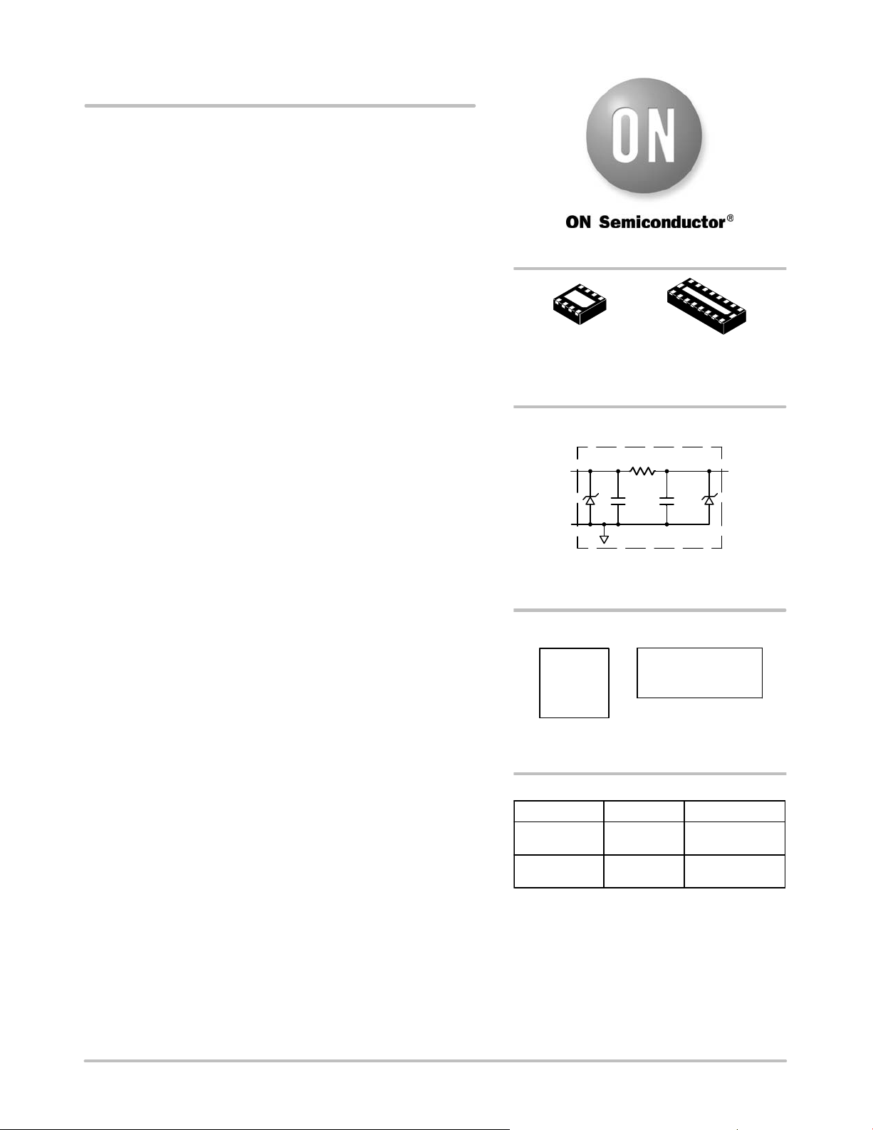
DE SUFFIX
CASE 511BE
FILTERn*
GND
http://onsemi.com
WDFN8
BLOCK DIAGRAM
15 pF
WDFN16
DE SUFFIX
CASE 511AU
200 W
FILTERn*
15 pF
Features
• Four and Eight Channels of EMI Filtering with ESD Protection
1 of 4/8 EMI Filtering + ESD Channels
See Package/Pinout Diagrams for Expanded Pin Information.
• Greater than 30 dB of Attenuation from 800 MHz to 3 GHz
• ±15 kV ESD Protection (IEC 61000−4−2, Contact Discharge)
MARKING DIAGRAM
• ±30 kV ESD Protection (HBM)
• Fabricated with Centuriont Advanced Low Capacitance Zener
Process Technology
N06
4E
N68E M
• Space Saving, Low−Profile 8 and 16−Lead WDFN Packages
• These Devices are Pb−Free and are RoHS Compliant
Applications
N06 4E = CM1406−04DE
N68E = CM1406−08DE
• I/O Port Protection for Mobile Handsets, Notebook Computers,
PDAs etc.
• EMI Filtering for Data Ports in Cell Phones, PDAs or Notebook
Computers
• EMI Filtering for LCD, Camera and Chip−to−Chip Data Lines
CM1406−04DE WDFN8
†For information on tape and reel specifications,
including part orientation and tape sizes, please
refer to our Tape and Reel Packaging Specification
Brochure, BRD8011/D.
ORDERING INFORMATION
Device Package Shipping
(Pb−Free)
WDFN16
(Pb−Free)
3000/Tape & Reel
3000/Tape & ReelCM1406−08DE
†
© Semiconductor Components Industries, LLC, 2011
March, 2011 − Rev. 3
1 Publication Order Number:
CM1406/D
Page 2
CM1406
PACKAGE / PINOUT DIAGRAMS
CM1406−04DE
8−Lead WDFN Package
CM1406−08DE
16−Lead WDFN Package
with Exposed End Pads
Pin 1
Marking
Top View
(Pins Down View)
87 65
N06
Pin 1
Marking
16 15 14 13 12 11 10 9
12 345678
4E
12 34
N68E
16 15 14 13 12 11 10 9
Bottom View
(Pins Up View)
1234
GND
PAD
8765
12345678
GND PAD
Table 1. PIN DESCRIPTIONS
Pins
1406−04Dx 1406−08Dx 1406−04Dx 1406−08Dx
1 1 FILTER1 Filter Channel 1 8 16 FILTER1 Filter Channel 1
2 2 FILTER2 Filter Channel 2 7 15 FILTER2 Filter Channel 2
3 3 FILTER3 Filter Channel 3 6 14 FILTER3 Filter Channel 3
4 4 FILTER4 Filter Channel 4 5 13 FILTER4 Filter Channel 4
5 FILTER5 Filter Channel 5 12 FILTER5 Filter Channel 5
6 FILTER6 Filter Channel 6 11 FILTER6 Filter Channel 6
7 FILTER7 Filter Channel 7 10 FILTER7 Filter Channel 7
8 FILTER8 Filter Channel 8 9 FILTER8 Filter Channel 8
GND Pad GND Device Ground
Name Description
Pins
Name Description
http://onsemi.com
2
Page 3
CM1406
SPECIFICATIONS
Table 2. ABSOLUTE MAXIMUM RATINGS
Parameter Rating Units
Storage Temperature Range –65 to +150 °C
DC Power per Resistor 100 mW
Package DC Power Rating 300 mW
Stresses exceeding Maximum Ratings may damage the device. Maximum Ratings are stress ratings only. Functional operation above the
Recommended Operating Conditions is not implied. Extended exposure to stresses above the Recommended Operating Conditions may affect
device reliability.
Table 3. STANDARD OPERATING CONDITIONS
Parameter Rating Units
Operating Temperature Range –40 to +85 °C
Table 4. ELECTRICAL OPERATING CHARACTERISTICS (Note 1)
Symbol Parameter Conditions Min Typ Max Units
R Resistance 160 200 240
C Capacitance At 2.5 V DC, 1 MHz, 30 mV AC 12 15 18 pF
V
DIODE
I
LEAK
V
V
SIG
ESD
Diode Standoff Voltage
Diode Leakage Current (Reverse Bias) V
Signal Voltage
Positive Clamp
Negative Clamp
In−system ESD Withstand Voltage
a) Human Body Model, MIL−STD−883,
I
= 10 mA
DIODE
= 3.3 V 0.1 1
DIODE
I
LOAD
I
LOAD
= 10 mA
= −10 mA
5.6
−1.5
(Note 2)
30
6.0 V
6.8
−0.8
Method 3015
b) Contact Discharge per
15
IEC 61000−4−2 Level 4
f
C
1. T
= 25°C unless otherwise specified.
A
2. ESD applied to input and output pins with respect to GND, one at a time.
Cut−off Frequency
SOURCE
= 50 W, Z
Z
LOAD
= 50 W
R = 200 W, C = 15 pF
105
9.0
−0.4
W
mA
V
kV
MHz
http://onsemi.com
3
Page 4
CM1406
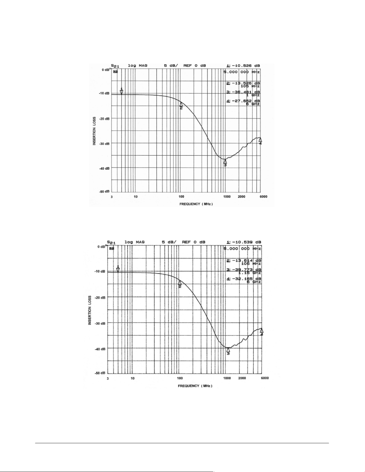
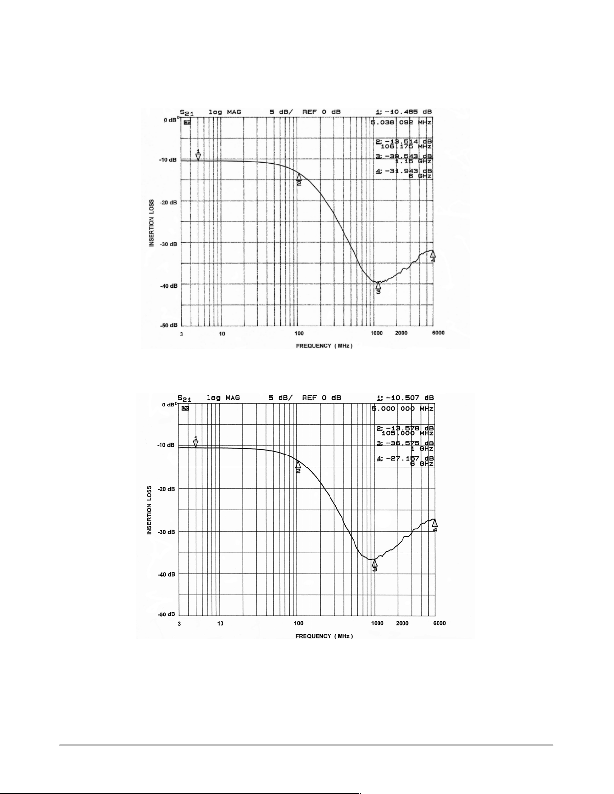
PERFORMANCE INFORMATION
Typical Filter Performance (nominal conditions unless specified otherwise, 0 V DC Bias, 50 W Environment)
Figure 1. Channel 1 EMI Filter Performance (CM1406−04 only)
Figure 2. Channel 2 EMI Filter Performance (CM1406−04 only)
http://onsemi.com
4
Page 5
CM1406
PERFORMANCE INFORMATION (Cont’d)
Typical Filter Performance (nominal conditions unless specified otherwise, 0 V DC Bias, 50 W Environment)
Figure 3. Channel 3 EMI Filter Performance (CM1406−04 only)
Figure 4. Channel 4 EMI Filter Performance (CM1406−04 only)
http://onsemi.com
5
Page 6

CM1406
PERFORMANCE INFORMATION (Cont’d)
Typical Filter Performance (nominal conditions unless specified otherwise, 0 V DC Bias, 50 W Environment)
Figure 5. Channel 1 EMI Filter Performance (CM1406−08 only)
Figure 6. Channel 2 EMI Filter Performance (CM1406−08 only)
http://onsemi.com
6
Page 7

CM1406
PERFORMANCE INFORMATION (Cont’d)
Typical Filter Performance (nominal conditions unless specified otherwise, 0 V DC Bias, 50 W Environment)
Figure 7. Channel 3 EMI Filter Performance (CM1406−08 only)
Figure 8. Channel 4 EMI Filter Performance (CM1406−08 only)
http://onsemi.com
7
Page 8

CM1406
PERFORMANCE INFORMATION (Cont’d)
Typical Filter Performance (nominal conditions unless specified otherwise, 0 V DC Bias, 50 W Environment)
Figure 9. Channel 5 EMI Filter Performance (CM1406−08 only)
Figure 10. Channel 6 EMI Filter Performance (CM1406−08 only)
http://onsemi.com
8
Page 9

CM1406
PERFORMANCE INFORMATION (Cont’d)
Typical Filter Performance (nominal conditions unless specified otherwise, 0 V DC Bias, 50 W Environment)
Figure 11. Channel 7 EMI Filter Performance (CM1406−08 only)
Figure 12. Channel 8 EMI Filter Performance (CM1406−08 only)
http://onsemi.com
9
Page 10

CM1406
PERFORMANCE INFORMATION (Cont’d)
Figure 13. Filter Capacitance vs. Input Voltage over Temperature
(normalized to capacitance at 2.5 V DC and 255C)
Centurion is a trademark of Semiconductor Components Industries, LLC (SCILLC).
http://onsemi.com
10
Page 11
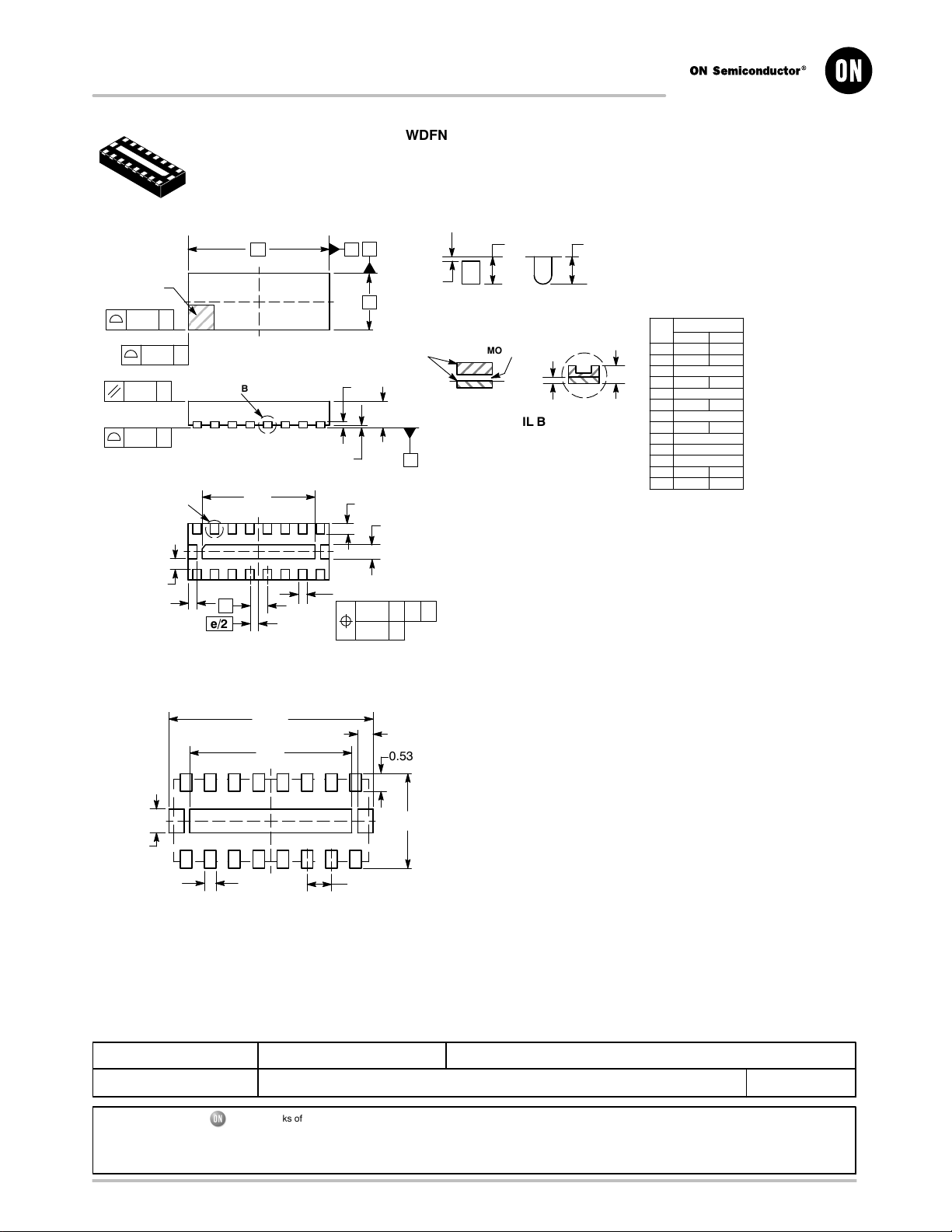
MECHANICAL CASE OUTLINE
PACKAGE DIMENSIONS
16
1
SCALE 4:1
B
A1
A
E
(A3)
16X
A
L
PIN ONE
REFERENCE
2X
0.10 C
2X
0.10 C
0.10 C
0.08 C
NOTE 4
DETAIL A
D
TOP VIEW
DETAIL B
SIDE VIEW
D2
18
WDFN16, 4x1.6, 0.5P
CASE 511AU−01
ISSUE O
L1
DETAIL A
ALTERNATE TERMINAL
CONSTRUCTIONS
MOLD CMPDEXPOSED Cu
CONSTRUCTIONS
E2
C
SEATING
PLANE
L
DETAIL B
ALTERNATE
A1
DATE 06 JUL 2010
NOTES:
1. DIMENSIONING AND TOLERANCING PER
L
ASME Y14.5M, 1994.
2. CONTROLLING DIMENSION: MILLIMETERS.
3. DIMENSION b APPLIES TO PLATED
TERMINAL AND IS MEASURED BETWEEN
0.15 AND 0.30 MM FROM TERMINAL TIP.
4. COPLANARITY APPLIES TO THE EXPOSED
PAD AS WELL AS THE TERMINALS.
MILLIMETERS
DIM MIN MAX
A3
A 0.70 0.80
A1 0.00 0.05
A3 0.20 REF
b 0.20 0.30
D 4.00 BSC
D2 3.10 3.30
E 1.60 BSC
E2 0.30 0.50
e 0.50 BSC
F 0.25 REF
K 0.30 REF
L 0.20 0.40
L1 −−− 0.15
K
F
e
e/2
916
16X
b
0.10 B
0.05ACC
NOTE 3
BOTTOM VIEW
RECOMMENDED
SOLDERING FOOTPRINT*
4.30
2X
0.35
3.30
3X
0.50
16X
0.30
DIMENSION: MILLIMETERS
*For additional information on our Pb−Free strategy and soldering
details, please download the ON Semiconductor Soldering and
Mounting Techniques Reference Manual, SOLDERRM/D.
0.50
PITCH
16X
0.53
1.90
DOCUMENT NUMBER:
DESCRIPTION:
ON Semiconductor and are trademarks of Semiconductor Components Industries, LLC dba ON Semiconductor or its subsidiaries in the United States and/or other countries.
ON Semiconductor reserves the right to make changes without further notice to any products herein. ON Semiconductor makes no warranty, representation or guarantee regarding
the suitability of its products for any particular purpose, nor does ON Semiconductor assume any liability arising out of the application or use of any product or circuit, and specifically
disclaims any and all liability, including without limitation special, consequential or incidental damages. ON Semiconductor does not convey any license under its patent rights nor the
rights of others.
© Semiconductor Components Industries, LLC, 2019
98AON48925E
WDFN16, 4X1.6, 0.5P
Electronic versions are uncontrolled except when accessed directly from the Document Repository.
Printed versions are uncontrolled except when stamped “CONTROLLED COPY” in red.
PAGE 1 OF 1
www.onsemi.com
Page 12

MECHANICAL CASE OUTLINE
PACKAGE DIMENSIONS
1
SCALE 2:1
B
DETAIL B
A1
4
5
A
8X
E
A
8X
E2
b
0.10 C
0.05 C
L
A3
8X
0.50
C
PIN ONE
REFERENCE
2X
2X
NOTE 4
DETAIL A
PACKAGE
OUTLINE
D
C0.10
C0.10
TOP VIEW
C0.10
C0.08
SIDE VIEW
D2
1
K
8
e
BOTTOM VIEW
RECOMMENDED
SOLDERING FOOTPRINT*
1.70
WDFN8 2x2, 0.5P
CASE 511BE−01
ISSUE A
L1
SEATING
PLANE
A
BB
NOTE 3
L
DETAIL A
ALTERNATE
CONSTRUCTIONS
MOLD CMPDEXPOSED Cu
DETAIL B
ALTERNATE
CONSTRUCTIONS
DATE 27 MAY 2011
L
NOTES:
1. DIMENSIONING AND TOLERANCING PER
ASME Y14.5M, 1994.
2. CONTROLLING DIMENSION: MILLIMETERS.
3. DIMENSION b APPLIES TO PLATED
TERMINAL AND IS MEASURED BETWEEN
0.15 AND 0.30 MM FROM TERMINAL TIP.
4. COPLANARITY APPLIES TO THE EXPOSED
PAD AS WELL AS THE TERMINALS.
MILLIMETERS
A3
A1
DIM MIN MAX
A 0.70 0.80
A1 0.00 0.05
A3 0.20 REF
b 0.20 0.30
D 2.00 BSC
D2 1.50 1.70
E 2.00 BSC
E2 0.80 1.00
e 0.50 BSC
K 0.25 REF
L 0.20 0.40
L1 −−− 0.15
GENERIC
MARKING DIAGRAM*
1
XX MG
G
XX = Specific Device Code
M = Date Code
G = Pb−Free Package
(Note: Microdot may be in either location)
*This information is generic. Please refer to
device data sheet for actual part marking.
Pb−Free indicator, “G” or microdot “ G”,
may or may not be present.
8X
0.30
2.30
1.00
0.50
PITCH
1
DIMENSIONS: MILLIMETERS
*For additional information on our Pb−Free strategy and soldering
details, please download the ON Semiconductor Soldering and
Mounting Techniques Reference Manual, SOLDERRM/D.
DOCUMENT NUMBER:
DESCRIPTION:
ON Semiconductor and are trademarks of Semiconductor Components Industries, LLC dba ON Semiconductor or its subsidiaries in the United States and/or other countries.
ON Semiconductor reserves the right to make changes without further notice to any products herein. ON Semiconductor makes no warranty, representation or guarantee regarding
the suitability of its products for any particular purpose, nor does ON Semiconductor assume any liability arising out of the application or use of any product or circuit, and specifically
disclaims any and all liability, including without limitation special, consequential or incidental damages. ON Semiconductor does not convey any license under its patent rights nor the
rights of others.
© Semiconductor Components Industries, LLC, 2019
98AON48936E
WDFN8, 2X2, 0.5P
Electronic versions are uncontrolled except when accessed directly from the Document Repository.
Printed versions are uncontrolled except when stamped “CONTROLLED COPY” in red.
PAGE 1 OF 1
www.onsemi.com
Page 13

ON Semiconductor and are trademarks of Semiconductor Components Industries, LLC dba ON Semiconductor or its subsidiaries in the United States and/or other countries.
ON Semiconductor owns the rights to a number of patents, trademarks, copyrights, trade secrets, and other intellectual property. A listing of ON Semiconductor ’s product/patent
coverage may be accessed at www.onsemi.com/site/pdf/Patent−Marking.pdf
ON Semiconductor makes no warranty, representation or guarantee regarding the suitability of its products for any particular purpose, nor does ON Semiconductor assume any liability
arising out of the application or use of any product or circuit, and specifically disclaims any and all liability, including without limitation special, consequential or incidental damages.
Buyer is responsible for its products and applications using ON Semiconductor products, including compliance with all laws, regulations and safety requirements or standards,
regardless of any support or applications information provided by ON Semiconductor. “Typical” parameters which may be provided in ON Semiconductor data sheets and/or
specifications can and do vary in different applications and actual performance may vary over time. All operating parameters, including “Typicals” must be validated for each customer
application by customer’s technical experts. ON Semiconductor does not convey any license under its patent rights nor the rights of others. ON Semiconductor products are not
designed, intended, or authorized for use as a critical component in life support systems or any FDA Class 3 medical devices or medical devices with a same or similar classification
in a foreign jurisdiction or any devices intended for implantation in the human body. Should Buyer purchase or use ON Semiconductor products for any such unintended or unauthorized
application, Buyer shall indemnify and hold ON Semiconductor and its officers, employees, subsidiaries, affiliates, and distributors harmless against all claims, costs, damages, and
expenses, and reasonable attorney fees arising out of, directly or indirectly, any claim of personal injury or death associated with such unintended or unauthorized use, even if such
claim alleges that ON Semiconductor was negligent regarding the design or manufacture of the part. ON Semiconductor is an Equal Opportunity/Affirmative Action Employer. This
literature is subject to all applicable copyright laws and is not for resale in any manner.
. ON Semiconductor reserves the right to make changes without further notice to any products herein.
PUBLICATION ORDERING INFORMATION
LITERATURE FULFILLMENT:
Email Requests to: orderlit@onsemi.com
ON Semiconductor Website: www.onsemi.com
TECHNICAL SUPPORT
North American Technical Support:
Voice Mail: 1 800−282−9855 Toll Free USA/Canada
Phone: 011 421 33 790 2910
Europe, Middle East and Africa Technical Support:
Phone: 00421 33 790 2910
For additional information, please contact your local Sales Representative
◊
www.onsemi.com
1
 Loading...