

Page 1
CM1241
4-Channel Low Capacitance
Dual-Voltage ESD Protection
Array
Features
• 3 Channels of Low Voltage ESD Protection
• 1 Channel of High Voltage ESD Protection
• Provides ESD Protection to IEC61000−4−2 Level 4:
±8 kV Contact Discharge (Pins 1−3)
±15 kV Contact Discharge (Pin 4)
• Low Channel Input Capacitance
• Minimal Capacitance Change with Temperature and Voltage
• High Voltage Zener Diode Protects Supply Rail
• No Need for External Bypass Capacitors
• Each I/O Pin Can Withstand Over 1000 ESD Strikes*
• These Devices are Pb−Free and are RoHS Compliant
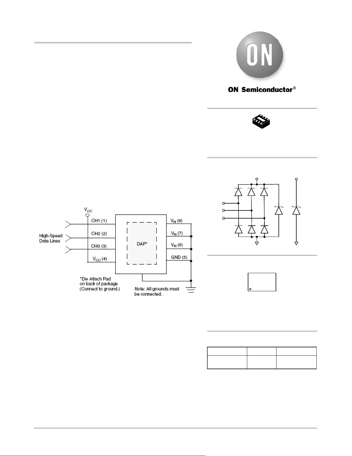
TYPICAL APPLICATION
CH1
CH2
CH3
http://onsemi.com
1
WDFN−8
D4 SUFFIX
CASE 511BF
BLOCK DIAGRAM
(Internal)
V
P
Pin 1
Pin 2
Pin 3
Pins 6 − 8
V
N
MARKING DIAGRAM
8
V
CC
Pin 4
Pin 5
GND
AW1 MG
G
AW1 = Specific Device Code
M = Date Code
G = Pb−Free Package
(Note: Microdot may be in either location)
ORDERING INFORMATION
Device Package Shipping
WDFN−8
(Pb−Free)
†For information on tape and reel specifications,
including part orientation and tape sizes, please
refer to our Tape and Reel Packaging Specification
Brochure, BRD8011/D.
*Standard test condition is IEC61000−4−2 level 4 test circuit with each pin subjected to ±8 kV contact discharge for 1000 pulses. Discharges
are timed at 1 second intervals and all 1000 strikes are completed in one continuous test run. The part is then subjected to standard production
test to verify that all of the tested parameters are within spec after the 1000 strikes.
© Semiconductor Components Industries, LLC, 2011
February, 2011 − Rev. 4
1 Publication Order Number:
3000/Tape & ReelCM1241−04D4
†
CM1241/D
Page 2
CM1241
Table 1. PIN DESCRIPTIONS
4−Channel, 8−Lead, WDFN−8 Package
Pin Name Type Description
1 CH1 I/O LV Low−capacitance ESD Channel
2 CH2 I/O LV Low−capacitance ESD Channel
3 CH3 I/O LV Low−capacitance ESD Channel
4 V
5 GND Ground
6 V
7 V
8 V
DAP GND Die Attach Pad (Ground)
HV VDDHV ESD Channel
CC
N
N
N
Negative Voltage Supply Rail
Negative Voltage Supply Rail
Negative Voltage Supply Rail
Pin 1
Marking
PACKAGE / PINOUT DIAGRAMS
Top View
(Pins Down View)
8 7 6 5
1 2 3 4
8−Lead WDFN
Bottom View
(Pins Up View)
1234
DAPAW1
8765
SPECIFICATIONS
Table 2. ABSOLUTE MAXIMUM RATINGS
Parameter Rating Units
DC Voltage on Low−voltage Pins 6.0 V
DC Voltage on High−voltage Pins (VCC pin) 14.5 V
Operating Temperature Range –40 to +85 °C
Storage Temperature Range –65 to +150 °C
Stresses exceeding Maximum Ratings may damage the device. Maximum Ratings are stress ratings only. Functional operation above the
Recommended Operating Conditions is not implied. Extended exposure to stresses above the Recommended Operating Conditions may affect
device reliability.
Table 3. STANDARD OPERATING CONDITIONS
Parameter Rating Units
Operating Temperature Range –40 to +85 °C
http://onsemi.com
2
Page 3

CM1241
Table 4. ELECTRICAL OPERATING CHARACTERISTICS (Note1)
Symbol
V
F
I
LEAK
C
IN
ΔC
IN
I
LEAK_HV
C
IN_HV
V
F_HV
LV Diode Reverse Voltage
(Positive Voltage)
LV Diode Forward Voltage
(Negative Voltage)
LV Channel Leakage Current
(Pins 1 and 2)
LV Channel Leakage Current
(Pin 3 only)
LV Channel Input Capacitance At 1 MHz, V
LV Channel Input Capacitance
Matching
HV Channel Leakage Current T
HV Channel Input Capacitance At 1 MHz, V
HV Diode Breakdown Voltage
Positive Voltage
Parameter Conditions Min Typ Max Units
I
= 10 mA; T
F
I
= 10 mA; T
F
= 25°C 6.8 8.2 9.2 V
A
= 25°C –1.05 –0.9 –0.6 V
A
TA = −30°C to 65°C; VIN = 3.3 V,
V
= 0 V
N
TA = −30°C to 65°C; VIN = 3.3 V,
V
= 0 V
N
= 0 V, VIN = 1.65 V 1.2 1.5 pF
N
At 1 MHz, V
= 25°C; V
A
I
= 10 mA; T
F
= 0 V, VIN = 1.65 V 0.02 pF
N
= 11 V, V
CC
= 0 V, VIN = 2.5 V 53 pF
N
= 25°C 14.6 17.7 V
A
= 0 V 0.1 1.0
N
100 nA
100 nA
mA
V
ESD
ESD Protection
Peak Discharge Voltage at any
channel input, in system
Contact discharge per
IEC 61000−4−2 standard
V
LV Channel Clamp Voltage (Pin 1−3)
CL
Positive Transients
Negative Transients
R
DYN
Dynamic Resistance
LV Channel Positive Transients
LV Channel Negative Transients
HV Channel Positive Transients
HV Channel Negative Transients
1. All parameters specified at T
T
= 25°C ±8 (Pin 1−3)
A
T
= 25°C, I
A
I
= 1 A, tP = 8/20 mS
PP
Any I/O pin to Ground
= –40°C to +85°C unless otherwise noted.
A
= 1 A, tP = 8/20 mS
PP
kV
±15 (Pin 4)
V
+9.64
–1.75
W
0.72
0.59
1.20
0.36
http://onsemi.com
3
Page 4

CM1241
PERFORMANCE INFORMATION
Input Channel Capacitance Performance Curves for Low Voltage Pins
Figure 1. Typical Variation of CIN vs. VIN
(Low Voltage Inputs, f = 1 MHz, V
= 0 V)
N
Figure 2. Typical Variation of CIN vs. Temp
(Low Voltage Inputs, f = 1 MHz, V
http://onsemi.com
4
= 0 V)
N
Page 5

CM1241
PERFORMANCE INFORMATION (Cont’d)
Typical Filter Performance for Low Voltage Pins
Nominal conditions unless specified; otherwise, 50 W environment.
Figure 3. Channel 1 vs. All GND Pins (0 V DC Bias)
Figure 4. Channel 2 vs. All GND Pins (0 V DC Bias)
http://onsemi.com
5
Page 6

CM1241
PERFORMANCE INFORMATION (Cont’d)
Typical Filter Performance for Low Voltage Pins
Nominal conditions unless specified; otherwise, 50 W environment.
Figure 5. Channel 3 vs. All GND Pins (0 V DC Bias)
http://onsemi.com
6
Page 7

MECHANICAL CASE OUTLINE
PACKAGE DIMENSIONS
8
1
SCALE 4:1
B
A1
A
8X
E
(A3)
A
SEATING
C
PLANE
L
E2
REFERENCE
2X
2X
NOTE 4
PIN ONE
0.10 C
0.10 C
0.10 C
0.08 C
DETAIL A
D
TOP VIEW
DETAIL B
SIDE VIEW
D2
14
WDFN8, 1.7x1.35, 0.4P
CASE 511BF−01
ISSUE O
L
L1
DETAIL A
ALTERNATE TERMINAL
CONSTRUCTIONS
MOLD CMPDEXPOSED Cu
DETAIL B
ALTERNATE
CONSTRUCTIONS
A1
DATE 21 JUL 2010
NOTES:
1. DIMENSIONING AND TOLERANCING PER
L
ASME Y14.5M, 1994.
2. CONTROLLING DIMENSION: MILLIMETERS.
3. DIMENSION b APPLIES TO PLATED
TERMINAL AND IS MEASURED BETWEEN
0.15 AND 0.30 MM FROM TERMINAL TIP.
4. COPLANARITY APPLIES TO THE EXPOSED
PAD AS WELL AS THE TERMINALS.
MILLIMETERS
DIM MIN MAX
A3
A 0.70 0.80
A1 0.00 0.05
A3 0.20 REF
b 0.15 0.25
D 1.7 BSC
D2 1.10 1.30
E 1.35 BSC
E2 0.30 0.50
e 0.40 BSC
K 0.22 REF
L 0.15 0.35
L1 −−− 0.15
K
e
e/2
58
8X
b
0.10 B
NOTE 3
0.05ACC
BOTTOM VIEW
RECOMMENDED
SOLDERING FOOTPRINT*
1.30
0.50
8X
0.25
DIMENSION: MILLIMETERS
*For additional information on our Pb−Free strategy and soldering
details, please download the ON Semiconductor Soldering and
Mounting Techniques Reference Manual, SOLDERRM/D.
8X
0.43
1.65
0.40
PITCH
DOCUMENT NUMBER:
DESCRIPTION:
ON Semiconductor and are trademarks of Semiconductor Components Industries, LLC dba ON Semiconductor or its subsidiaries in the United States and/or other countries.
ON Semiconductor reserves the right to make changes without further notice to any products herein. ON Semiconductor makes no warranty, representation or guarantee regarding
the suitability of its products for any particular purpose, nor does ON Semiconductor assume any liability arising out of the application or use of any product or circuit, and specifically
disclaims any and all liability, including without limitation special, consequential or incidental damages. ON Semiconductor does not convey any license under its patent rights nor the
rights of others.
© Semiconductor Components Industries, LLC, 2019
98AON48937E
WDFN8, 1.7X1.35, 0.4P
Electronic versions are uncontrolled except when accessed directly from the Document Repository.
Printed versions are uncontrolled except when stamped “CONTROLLED COPY” in red.
PAGE 1 OF 1
www.onsemi.com
Page 8

ON Semiconductor and are trademarks of Semiconductor Components Industries, LLC dba ON Semiconductor or its subsidiaries in the United States and/or other countries.
ON Semiconductor owns the rights to a number of patents, trademarks, copyrights, trade secrets, and other intellectual property. A listing of ON Semiconductor’s product/patent
coverage may be accessed at www.onsemi.com/site/pdf/Patent−Marking.pdf
ON Semiconductor makes no warranty, representation or guarantee regarding the suitability of its products for any particular purpose, nor does ON Semiconductor assume any liability
arising out of the application or use of any product or circuit, and specifically disclaims any and all liability, including without limitation special, consequential or incidental damages.
Buyer is responsible for its products and applications using ON Semiconductor products, including compliance with all laws, regulations and safety requirements or standards,
regardless of any support or applications information provided by ON Semiconductor. “Typical” parameters which may be provided in ON Semiconductor data sheets and/or
specifications can and do vary in different applications and actual performance may vary over time. All operating parameters, including “Typicals” must be validated for each customer
application by customer’s technical experts. ON Semiconductor does not convey any license under its patent rights nor the rights of others. ON Semiconductor products are not
designed, intended, or authorized for use as a critical component in life support systems or any FDA Class 3 medical devices or medical devices with a same or similar classification
in a foreign jurisdiction or any devices intended for implantation in the human body. Should Buyer purchase or use ON Semiconductor products for any such unintended or unauthorized
application, Buyer shall indemnify and hold ON Semiconductor and its officers, employees, subsidiaries, affiliates, and distributors harmless against all claims, costs, damages, and
expenses, and reasonable attorney fees arising out of, directly or indirectly, any claim of personal injury or death associated with such unintended or unauthorized use, even if such
claim alleges that ON Semiconductor was negligent regarding the design or manufacture of the part. ON Semiconductor is an Equal Opportunity/Affirmative Action Employer. This
literature is subject to all applicable copyright laws and is not for resale in any manner.
. ON Semiconductor reserves the right to make changes without further notice to any products herein.
PUBLICATION ORDERING INFORMATION
LITERATURE FULFILLMENT:
Email Requests to: orderlit@onsemi.com
ON Semiconductor Website: www.onsemi.com
TECHNICAL SUPPORT
North American Technical Support:
Voice Mail: 1 800−282−9855 Toll Free USA/Canada
Phone: 011 421 33 790 2910
Europe, Middle East and Africa Technical Support:
Phone: 00421 33 790 2910
For additional information, please contact your local Sales Representative
◊
www.onsemi.com
1
 Loading...