

Page 1
CAV24C128
EEPROM Serial 128-Kb I2C
- Automotive Grade 1
Description
The CAV24C128 is a EEPROM Serial 128−Kb I2C, internally
organized as 16,384 words of 8 bits each.
It features a 64−byte page write buffer and supports both the
Standard (100 kHz), Fast (400 kHz) and Fast−Plus (1 MHz) I
protocol.
Write operations can be inhibited by taking the WP pin High (this
protects the entire memory).
On−Chip ECC (Error Correction Code) makes the device suitable
for high reliability applications.
Features
• Automotive AEC−Q100 Grade 1 (−40°C to +125°C) Qualified
• Supports Standard, Fast and Fast−Plus I
• 2.5 V to 5.5 V Supply Voltage Range
• 64−Byte Page Write Buffer
• Hardware Write Protection for Entire Memory
• Schmitt Triggers and Noise Suppression Filters on I
(SCL and SDA)
• Low Power CMOS Technology
• 1,000,000 Program/Erase Cycles
• 100 Year Data Retention
• 8−lead SOIC and TSSOP Packages
• This Device is Pb−Free, Halogen Free/BFR Free and RoHS
Compliant*
V
CC
2
C Protocol
2
C Bus Inputs
www.onsemi.com
2
C
TSSOP−8
Y SUFFIX
CASE 948AL
SOIC−8
W SUFFIX
CASE 751BD
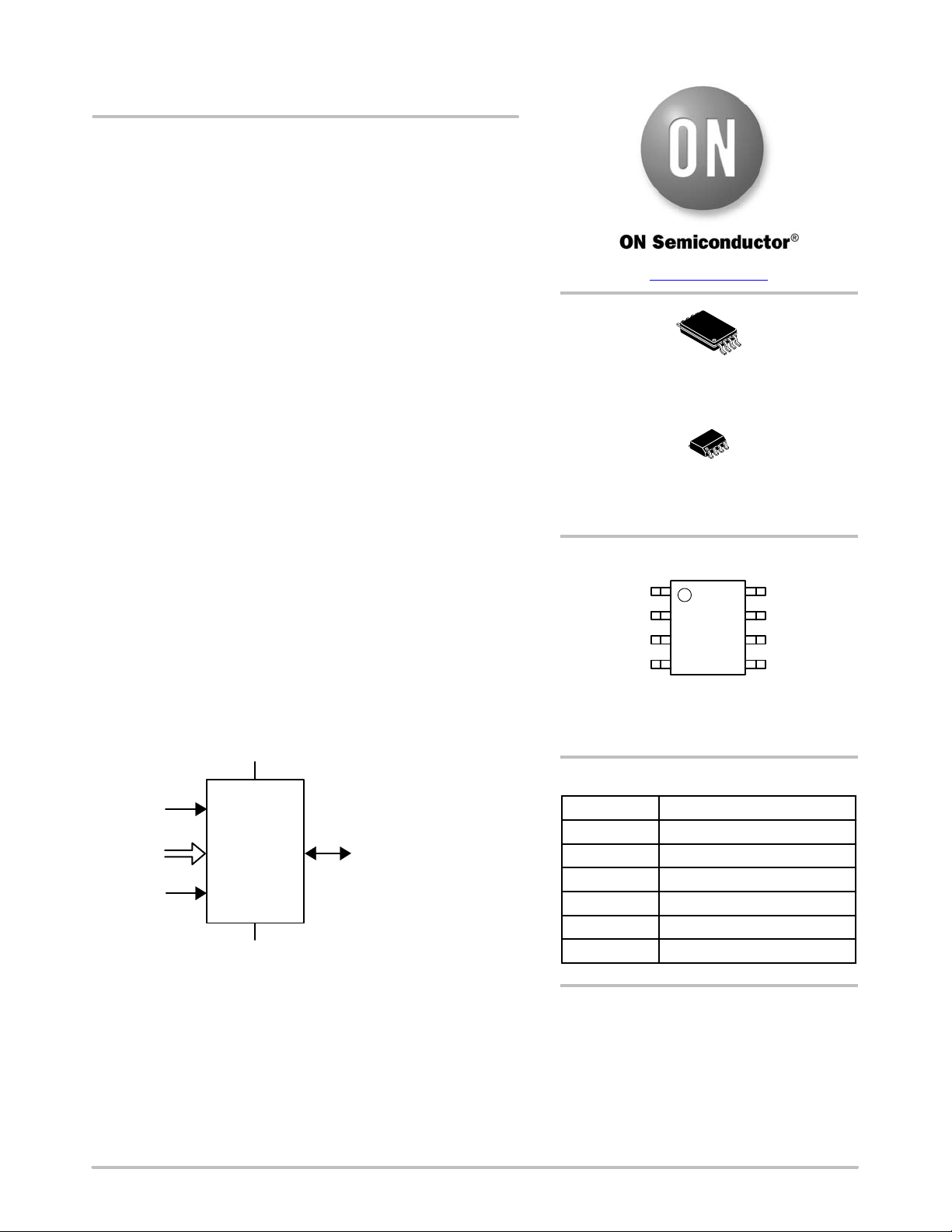
PIN CONFIGURATION
A
0
A
1
A
2
V
SS
SOIC (W), TSSOP (Y)
For the location of Pin 1, please consult the
corresponding package drawing.
1
V
CC
WP
SCL
SDA
SCL
A2, A1, A
WP
0
CAV24C128
V
SS
SDA
Figure 1. Functional Symbol
* For additional information on our Pb−Free strategy and soldering details, please
download the ON Semiconductor Soldering and Mounting Techniques
Reference Manual, SOLDERRM/D.
© Semiconductor Components Industries, LLC, 2012
April, 2019 − Rev. 2
1 Publication Order Number:
PIN FUNCTION
FunctionPin Name
Device Address InputsA0, A1, A
2
Serial Data Input/OutputSDA
Serial Clock InputSCL
Write Protect InputWP
CC
SS
Power SupplyV
GroundV
ORDERING INFORMATION
See detailed ordering and shipping information in the package
dimensions section on page 11 of this data sheet.
CAV24C128/D
Page 2
CAV24C128
Table 1. ABSOLUTE MAXIMUM RATINGS
Parameter Rating Units
Storage Temperature −65 to +150 °C
Voltage on Any Pin with Respect to Ground (Note 1) −0.5 to +6.5 V
Stresses exceeding those listed in the Maximum Ratings table may damage the device. If any of these limits are exceeded, device functionality
should not be assumed, damage may occur and reliability may be affected.
1. The DC input voltage on any pin should not be lower than −0.5 V or higher than V
undershoot to no less than −1.5 V or overshoot to no more than V
+ 1.5 V, for periods of less than 20 ns.
CC
Table 2. RELIABILITY CHARACTERISTICS (Note 2)
Symbol Parameter Min Units
N
(Notes 3, 4) Endurance 1,000,000 Program / Erase Cycles
END
T
DR
2. These parameters are tested initially and after a design or process change that affects the parameter according to appropriate AEC−Q100
and JEDEC test methods.
3. Page Mode, V
4. This device uses ECC (Error Correction Code) logic with 6 ECC bits to correct one bit error in 4 data bytes. Therefore, when a single byte
has to be written, 4 bytes (including the ECC bits) are re−programmed. It is recommended to write by multiple of 4 bytes in order to benefit
from the maximum number of write cycles.
Data Retention 100 Years
= 5 V, 25°C
CC
+ 0.5 V. During transitions, the voltage on any pin may
CC
Table 3. D.C. OPERATING CHARACTERISTICS (V
Symbol
I
CCR
I
CCW
I
SB
I
L
V
IL
V
IH
V
OL
Parameter Test Conditions Min Max Units
Read Current Read, f
= 400 kHz/1 MHz 1 mA
SCL
Write Current 3 mA
Standby Current All I/O Pins at GND or V
I/O Pin Leakage Pin at GND or V
Input Low Voltage −0.5 0.3 V
Input High Voltage 0.7 V
Output Low Voltage IOL = 3.0 mA 0.4 V
Table 4. PIN IMPEDANCE CHARACTERISTICS (V
= 2.5 V to 5.5 V, TA = −40°C to +125°C, unless otherwise specified.)
CC
CC
CC
= 2.5 V to 5.5 V, TA = −40°C to +125°C, unless otherwise specified.)
CC
TA = −40°C to +125°C 5
TA = −40°C to +125°C 2
CC
VCC + 0.5 V
CC
mA
mA
V
Symbol Parameter Conditions Max Units
CIN (Note 5) SDA I/O Pin Capacitance VIN = 0 V 8 pF
CIN (Note 5) Input Capacitance (other pins) VIN = 0 V 6 pF
IWP, IA (Note 6) WP Input Current, Address Input
Current (A
, A1, A2)
0
V
< VIH, VCC = 5.5 V 75 mA
IN
V
< VIH, VCC = 3.3 V 50
IN
V
> V
IN
IH
2
5. These parameters are tested initially and after a design or process change that affects the parameter according to appropriate AEC−Q100
and JEDEC test methods.
6. When not driven, the WP, A
strong; therefore the external driver must be able to supply the pull−down current when attempting to drive the input HIGH. To conserve power,
as the input level exceeds the trip point of the CMOS input buffer (~ 0.5 x V
, A1, A2 pins are pulled down to GND internally. For improved noise immunity, the internal pull−down is relatively
0
), the strong pull−down reverts to a weak current source.
CC
www.onsemi.com
2
Page 3
CAV24C128
Table 5. A.C. CHARACTERISTICS (V
= 2.5 V to 5.5 V, TA = −40°C to +125°C) (Note 7)
CC
Standard Fast Fast−Plus
Symbol
F
SCL
t
HD:STA
t
LOW
t
HIGH
t
SU:STA
t
HD:DAT
t
SU:DAT
Parameter
Clock Frequency 100 400 1,000 kHz
START Condition Hold Time 4 0.6 0.25
Low Period of SCL Clock 4.7 1.3 0.45
High Period of SCL Clock 4 0.6 0.40
START Condition Setup Time 4.7 0.6 0.25
Data In Hold Time 0 0 0
Data In Setup Time 250 100 50 ns
Min Max Min Max Min Max
tR (Note 8) SDA and SCL Rise Time 1,000 300 100 ns
tF (Note 8) SDA and SCL Fall Time 300 300 100 ns
t
SU:STO
t
BUF
t
AA
t
DH
Ti (Note 8) Noise Pulse Filtered at SCL
STOP Condition Setup Time 4 0.6 0.25
Bus Free Time Between
4.7 1.3 0.5
STOP and START
SCL Low to Data Out Valid 3.5 0.9 0.40
Data Out Hold Time 100 100 50 ns
100 100 50 ns
and SDA Inputs
t
SU:WP
t
HD:WP
t
WR
t
PU
(Notes 8, 9)
WP Setup Time 0 0 0
WP Hold Time 2.5 2.5 1
Write Cycle Time 5 5 5 ms
Power-up to Ready Mode 1 1 0.1 1 ms
7. Test conditions according to “A.C. Test Conditions” table.
8. Tested initially and after a design or process change that affects this parameter.
is the delay between the time VCC is stable and the device is ready to accept commands.
9. t
PU
Units
ms
ms
ms
ms
ms
ms
ms
ms
ms
ms
Table 6. A.C. TEST CONDITIONS
Input Levels 0.2 x VCC to 0.8 x V
Input Rise and Fall Times v 50 ns
Input Reference Levels 0.3 x VCC, 0.7 x V
Output Reference Levels 0.5 x V
CC
Output Load Current Source: IOL = 3 mA; CL = 100 pF
CC
CC
www.onsemi.com
3
Page 4

CAV24C128
Power−On Reset (POR)
The CAV24C128 incorporates Power−On Reset (POR)
circuitry which protects the device against powering up in
the wrong state.
The CAV24C128 will power up into Standby mode after
V
exceeds the POR trigger level and will power down into
CC
Reset mode when V
drops below the POR trigger level.
CC
This bi−directional POR feature protects the device against
‘brown−out’ failure following a temporary loss of power.
Pin Description
SCL: The Serial Clock input pin accepts the Serial Clock
generated by the Master.
SDA: The Serial Data I/O pin receives input data and
transmits data stored in EEPROM. In transmit mode, this pin
is open drain. Data is acquired on the positive edge, and is
delivered on the negative edge of SCL.
A
, A1 and A2: The Address pins accept the device address.
0
When not driven, these pins are pulled LOW internally.
WP: The Write Protect input pin inhibits all write
operations, when pulled HIGH. When not driven, this pin is
pulled LOW internally.
Functional Description
The CAV24C128 supports the Inter−Integrated Circuit
(I2C) Bus data transmission protocol, which defines a device
that sends data to the bus as a transmitter and a device
receiving data as a receiver. Data flow is controlled by a
Master device, which generates the serial clock and all
START and STOP conditions. The CAV24C128 acts as a
Slave device. Master and Slave alternate as either
transmitter or receiver. Up to 8 devices may be connected to
the bus as determined by the device address inputs A
and A
.
2
2
C Bus Protocol
I
two wires are connected to the V
2
The I
C bus consists of two ‘wires’, SCL and SDA. The
supply via pull−up
CC
, A1,
0
resistors. Master and Slave devices connect to the 2−wire
bus via their respective SCL and SDA pins. The transmitting
device pulls down the SDA line to ‘transmit’ a ‘0’ and
releases it to ‘transmit’ a ‘1’.
Data transfer may be initiated only when the bus is not
busy (see A.C. Characteristics).
During data transfer, the SDA line must remain stable
while the SCL line is HIGH. An SDA transition while SCL
is HIGH will be interpreted as a START or STOP condition
(Figure 2). The START condition precedes all commands. It
consists of a HIGH to LOW transition on SDA while SCL
is HIGH. The START acts as a ‘wake−up’ call to all
receivers. Absent a START, a Slave will not respond to
commands. The STOP condition completes all commands.
It consists of a LOW to HIGH transition on SDA while SCL
is HIGH.
Device Addressing
The Master initiates data transfer by creating a START
condition on the bus. The Master then broadcasts an 8−bit
serial Slave address. The first 4 bits of the Slave address are
set to 1010, for normal Read/Write operations (Figure 3).
The next 3 bits, A
, A1 and A0, select one of 8 possible Slave
2
devices and must match the state of the external address pins.
The last bit, R/W
, specifies whether a Read (1) or Write (0)
operation is to be performed.
Acknowledge
After processing the Slave address, the Slave responds
with an acknowledge (ACK) by pulling down the SDA line
th
during the 9
clock cycle (Figure 4). The Slave will also
acknowledge all address bytes and every data byte presented
in Write mode. In Read mode the Slave shifts out a data byte,
and then releases the SDA line during the 9
th
clock cycle. As
long as the Master acknowledges the data, the Slave will
continue transmitting. The Master terminates the session by
not acknowledging the last data byte (NoACK) and by
issuing a STOP condition. Bus timing is illustrated in
Figure 5.
www.onsemi.com
4
Page 5

SCL
)
SDA
CAV24C128
SCL FROM
MASTER
DATA OUTPUT
FROM TRANSMITTER
DATA OUTPUT
FROM RECEIVER
START
CONDITION
Figure 2. START/STOP Conditions
101 0
Figure 3. Slave Address Bits
BUS RELEASE DELAY (TRANSMITTER)
189
START
ACK DELAY (≤ tAA)
DEVICE ADDRESS
A2A
1
A0R/W
STOP
CONDITION
BUS RELEASE DELAY (RECEIVER
ACK SETUP (≥ t
SU:DAT
)
SCL
SDA IN
SDA OUT
t
SU:STA
Figure 4. Acknowledge Timing
t
F
t
LOW
t
HD:STA
t
HIGH
t
LOW
t
HD:DAT
t
AA
t
R
t
SU:DAT
t
DH
t
SU:STO
t
BUF
Figure 5. Bus Timing
www.onsemi.com
5
Page 6

CAV24C128
Write Operations
Byte Write
Upon receiving a Slave address with the R/W bit set to ‘0’,
the CAV24C128 will interpret the next two bytes as address
bytes. These bytes are used to initialize the internal address
counter; the 2 most significant bits are ‘don’t care’, the next
8 point to one of 256 available pages and the last 6 point to
a location within a 64 byte page. A byte following the
address bytes will be interpreted as data. The data will be
loaded into the Page Write Buffer and will eventually be
written to memory at the address specified by the 14 active
address bits provided earlier. The CAV24C128 will
acknowledge the Slave address, address bytes and data byte.
The Master then starts the internal Write cycle by issuing a
STOP condition (Figure 6). During the internal Write cycle
(t
), the SDA output will be tri−stated and additional Read
WR
or Write requests will be ignored (Figure 7).
Page Write
By continuing to load data into the Page Write Buffer after
st
the 1
data byte and before issuing the STOP condition, up
to 64 bytes can be written simultaneously during one
internal Write cycle (Figure 8). If more data bytes are loaded
than locations available to the end of page, then loading will
continue from the beginning of page, i.e. the page address is
latched and the address count automatically increments to
and then wraps−around at the page boundary. Previously
loaded data can thus be overwritten by new data. What is
eventually written to memory reflects the latest Page Write
Buffer contents. Only data loaded within the most recent
Page Write sequence will be written to memory.
Acknowledge Polling
The ready/busy status of the CAV24C128 can be
ascertained by sending Read or Write requests immediately
following the STOP condition that initiated the internal
Write cycle. As long as internal Write is in progress, the
CAV24C128 will not acknowledge the Slave address.
Hardware Write Protection
With the WP pin held HIGH, the entire memory is
protected against Write operations. If the WP pin is left
floating or is grounded, it has no impact on the operation of
the CAV24C128. The state of the WP pin is strobed on the
last falling edge of SCL immediately preceding the first data
byte (Figure 9). If the WP pin is HIGH during the strobe
interval, the CAV24C128 will not acknowledge the data
byte and the Write request will be rejected.
Delivery State
The CAV24C128 is shipped erased, i.e., all bytes are FFh.
SCL
SDA
BUS ACTIVITY:
MASTER
SLAVE
S
T
A
SLAVE
R
ADDRESS
T
S
* = Don’t Care Bit
8th Bit
Byte n
A
C
K
**
ADDRESS
BYTE
a
13−a8
A
C
K
ADDRESS
BYTE
a7−a
Figure 6. Byte Write Sequence
ACK
t
WR
STOP
CONDITION
Figure 7. Write Cycle Timing
S
DATA
A
C
K
START
CONDITION
BYTE
0
T
O
P
P
A
C
K
ADDRESS
www.onsemi.com
6
Page 7

CAV24C128
BUS ACTIVITY:
MASTER
SLAVE
* = Don’t Care Bit
P v 63
S
T
A
R
T
S
SLAVE
ADDRESS
SCL
SDA
WP
A
C
K
**
ADDRESS
BYTE
a
13−a8
A
C
K
ADDRESS
BYTE
a7−a
0
DATA
BYTE
n
A
C
K
DATA
BYTE
n+1
A
C
K
A
C
K
DATA
BYTE
A
C
K
Figure 8. Page Write Sequence
ADDRESS
BYTE
1891 8
a
7
a
0
t
SU:WP
d
7
DATA
BYTE
d
0
n+P
S
T
O
P
P
A
C
K
Figure 9. WP Timing
Read Operations
Immediate Read
Upon receiving a Slave address with the R/W bit set to ‘1’,
the CAV24C128 will interpret this as a request for data
residing at the current byte address in memory. The
CAV24C128 will acknowledge the Slave address, will
immediately shift out the data residing at the current address,
and will then wait for the Master to respond. If the Master
does not acknowledge the data (NoACK) and then follows
up with a STOP condition (Figure 10), the CAV24C128
returns to Standby mode.
Selective Read
To read data residing at a specific location, the internal
address counter must first be initialized as described under
Byte Write. If rather than following up the two address bytes
t
HD:WP
with data, the Master instead follows up with an Immediate
Read sequence, then the CAV24C128 will use the 14 active
address bits to initialize the internal address counter and will
shift out data residing at the corresponding location. If the
Master does not acknowledge the data (NoACK) and then
follows up with a STOP condition (Figure 11), the
CAV24C128 returns to Standby mode.
Sequential Read
If during a Read session the Master acknowledges the 1
data byte, then the CAV24C128 will continue transmitting
data residing at subsequent locations until the Master
responds with a NoACK, followed by a STOP (Figure 12).
In contrast to Page Write, during Sequential Read the
address count will automatically increment to and then
wrap−around at end of memory (rather than end of page).
st
www.onsemi.com
7
Page 8

CAV24C128
SCL
SDA 8th Bit
BUS ACTIVITY:
MASTER
SLAVE
* = Don’t Care Bit
S
T
A
R
T
S
BUS ACTIVITY:
SLAVE
ADDRESS
N
O
A
C
K
MASTER
SLAVE
S
T
A
SLAVE
R
ADDRESS
T
S
A
DATA
C
K
BYTE
8
9
NO ACKDATA OUT
Figure 10. Immediate Read Sequence and Timing
S
A
C
K
**
ADDRESS
BYTE
a
13−a8
A
C
K
ADDRESS
BYTE
a7−a
0
A
C
K
T
A
R
T
S
SLAVE
ADDRESS
Figure 11. Selective Read Sequence
S
T
O
P
P
STOP
N
S
O
T
A
O
C
P
K
P
A
DATA
C
BYTE
K
BUS ACTIVITY:
MASTER
SLAVE
SLAVE
ADDRESS
A
DATA
C
BYTE
K
n
A
DATA
C
BYTE
K
n+1
Figure 12. Sequential Read Sequence
www.onsemi.com
8
N
O
S
T
A
O
C
P
K
P
A
DATA
C
BYTE
K
n+2
A
C
K
DATA
BYTE
n+x
Page 9

CAV24C128
ORDERING INFORMATION (Notes 10 thru 13)
Specific
Device
Device Order Number
CAV24C128WE−GT3 24128C SOIC−8,
CAV24C128YE−GT3 C28C TSSOP−8 E = Extended
†For information on tape and reel specifications, including part orientation and tape sizes, please refer to our Tape and Reel Packaging
Specifications Brochure, BRD8011/D.
10.All packages are RoHS−compliant (Lead−free, Halogen−free).
11. The standard lead finish is NiPdAu.
12.For additional package and temperature options, please contact your nearest ON Semiconductor Sales office.
13.For detailed information and a breakdown of device nomenclature and numbering systems, please see the ON Semiconductor Device
Nomenclature document, TND310/D, available at www.onsemi.com
Marking
Package
Type
JEDEC
Temperature Range Lead Finish Shipping
E = Extended
(−40°C to +125°C)
(−40°C to +125°C)
NiPdAu Tape & Reel,
3,000 Units / Reel
NiPdAu Tape & Reel,
3,000 Units / Reel
†
ON Semiconductor is licensed by the Philips Corporation to carry the I2C bus protocol.
www.onsemi.com
11
Page 10

MECHANICAL CASE OUTLINE
PACKAGE DIMENSIONS
E1 E
PIN # 1
IDENTIFICATION
SOIC 8, 150 mils
CASE 751BD−01
ISSUE O
DATE 19 DEC 2008
SYMBOL MIN NOM MAX
A
A1
b
c
D
E
E1
e
h
L
θ
1.35
0.10
0.33
0.19
4.80
5.80
3.80
1.27 BSC
0.25
0.40 1.27
1.75
0.25
0.51
0.25
5.00
6.20
4.00
0.50
0º 8º
TOP VIEW
D
A1
A
e
SIDE VIEW
Notes:
(1) All dimensions are in millimeters. Angles in degrees.
(2) Complies with JEDEC MS-012.
b
h
θ
c
L
END VIEW
DOCUMENT NUMBER:
DESCRIPTION:
ON Semiconductor and are trademarks of Semiconductor Components Industries, LLC dba ON Semiconductor or its subsidiaries in the United States and/or other countries.
ON Semiconductor reserves the right to make changes without further notice to any products herein. ON Semiconductor makes no warranty, representation or guarantee regarding
the suitability of its products for any particular purpose, nor does ON Semiconductor assume any liability arising out of the application or use of any product or circuit, and specifically
disclaims any and all liability, including without limitation special, consequential or incidental damages. ON Semiconductor does not convey any license under its patent rights nor the
rights of others.
© Semiconductor Components Industries, LLC, 2019
98AON34272E
SOIC 8, 150 MILS
Electronic versions are uncontrolled except when accessed directly from the Document Repository.
Printed versions are uncontrolled except when stamped “CONTROLLED COPY” in red.
PAGE 1 OF 1
www.onsemi.com
Page 11

MECHANICAL CASE OUTLINE
PACKAGE DIMENSIONS
b
E
E1
TSSOP8, 4.4x3
CASE 948AL−01
ISSUE O
SYMBOLθMIN NOM MAX
A1
A2
E1
L1
DATE 19 DEC 2008
A
0.05
0.80
b
c
D
E
e
L
0.19
0.09
2.90
6.30
4.30
0.50
0.90
3.00
6.40
4.40
0.65 BSC
1.00 REF
0.60
1.20
0.15
1.05
0.30
0.20
3.10
6.50
4.50
0.75
0º 8º
e
TOP VIEW
D
A2
SIDE VIEW
Notes:
(1) All dimensions are in millimeters. Angles in degrees.
(2) Complies with JEDEC MO-153.
A
A1
q1
L1
c
L
END VIEW
DOCUMENT NUMBER:
DESCRIPTION:
ON Semiconductor and are trademarks of Semiconductor Components Industries, LLC dba ON Semiconductor or its subsidiaries in the United States and/or other countries.
ON Semiconductor reserves the right to make changes without further notice to any products herein. ON Semiconductor makes no warranty, representation or guarantee regarding
the suitability of its products for any particular purpose, nor does ON Semiconductor assume any liability arising out of the application or use of any product or circuit, and specifically
disclaims any and all liability, including without limitation special, consequential or incidental damages. ON Semiconductor does not convey any license under its patent rights nor the
rights of others.
© Semiconductor Components Industries, LLC, 2019
98AON34428E
TSSOP8, 4.4X3
Electronic versions are uncontrolled except when accessed directly from the Document Repository.
Printed versions are uncontrolled except when stamped “CONTROLLED COPY” in red.
PAGE 1 OF 1
www.onsemi.com
Page 12

ON Semiconductor and are trademarks of Semiconductor Components Industries, LLC dba ON Semiconductor or its subsidiaries in the United States and/or other countries.
ON Semiconductor owns the rights to a number of patents, trademarks, copyrights, trade secrets, and other intellectual property. A listing of ON Semiconductor ’s product/patent
coverage may be accessed at www.onsemi.com/site/pdf/Patent−Marking.pdf
ON Semiconductor makes no warranty, representation or guarantee regarding the suitability of its products for any particular purpose, nor does ON Semiconductor assume any liability
arising out of the application or use of any product or circuit, and specifically disclaims any and all liability, including without limitation special, consequential or incidental damages.
Buyer is responsible for its products and applications using ON Semiconductor products, including compliance with all laws, regulations and safety requirements or standards,
regardless of any support or applications information provided by ON Semiconductor. “Typical” parameters which may be provided in ON Semiconductor data sheets and/or
specifications can and do vary in different applications and actual performance may vary over time. All operating parameters, including “Typicals” must be validated for each customer
application by customer’s technical experts. ON Semiconductor does not convey any license under its patent rights nor the rights of others. ON Semiconductor products are not
designed, intended, or authorized for use as a critical component in life support systems or any FDA Class 3 medical devices or medical devices with a same or similar classification
in a foreign jurisdiction or any devices intended for implantation in the human body. Should Buyer purchase or use ON Semiconductor products for any such unintended or unauthorized
application, Buyer shall indemnify and hold ON Semiconductor and its officers, employees, subsidiaries, affiliates, and distributors harmless against all claims, costs, damages, and
expenses, and reasonable attorney fees arising out of, directly or indirectly, any claim of personal injury or death associated with such unintended or unauthorized use, even if such
claim alleges that ON Semiconductor was negligent regarding the design or manufacture of the part. ON Semiconductor is an Equal Opportunity/Affirmative Action Employer. This
literature is subject to all applicable copyright laws and is not for resale in any manner.
. ON Semiconductor reserves the right to make changes without further notice to any products herein.
PUBLICATION ORDERING INFORMATION
LITERATURE FULFILLMENT:
Email Requests to: orderlit@onsemi.com
ON Semiconductor Website: www.onsemi.com
TECHNICAL SUPPORT
North American Technical Support:
Voice Mail: 1 800−282−9855 Toll Free USA/Canada
Phone: 011 421 33 790 2910
Europe, Middle East and Africa Technical Support:
Phone: 00421 33 790 2910
For additional information, please contact your local Sales Representative
◊
www.onsemi.com
1
 Loading...