

Page 1
CAT6241
LDO Voltage Regulator -
Adjustable CMOS
1 A
Description
The CAT6241 is a low dropout CMOS voltage regulator providing
up to 1000 mA of output current with fast response to load current and
line voltage changes. CAT6241 offers a user adjustable output voltage
from 0.5 V to 5.0 V and its low quiescent current make CAT6241 ideal
for energy conscious designs. CAT6241 is available in space saving
2 mm x 2 mm UDFN−8 and 3 mm x 3 mm WDFN−6 packages, each
with a power pad for heat sinking to the PCB.
Features
• Guaranteed 1000 mA Continuous Output Current
• V
: 0.5 V to 5.0 V, Minimum VIN: 1.6 V
OUT
• Dropout Voltage of 350 mV Typical at 1000 mA
• ±2.0% Output Voltage Accuracy at Room Temperature
• No−load Ground Current of 70 mA Typical
• Full−load Ground Current of 140 mA Typical
• “Zero” Current Shutdown Mode
• Under Voltage Lockout
• Stable with Ceramic Output Capacitors
• Current Limit and Thermal Protection
• 2 mm x 2 mm UDFN−8 and 3 mm x 3 mm WDFN−6 Packages
• These Devices are Pb−Free, Halogen Free/BFR Free and are RoHS
Compliant
Typical Applications
• DSP Core and I/O Voltages
• FPGAs, ASICs
• PDAs, Mobile Phones, GPS
• Camcorders and Cameras
• Hard Disk Drives
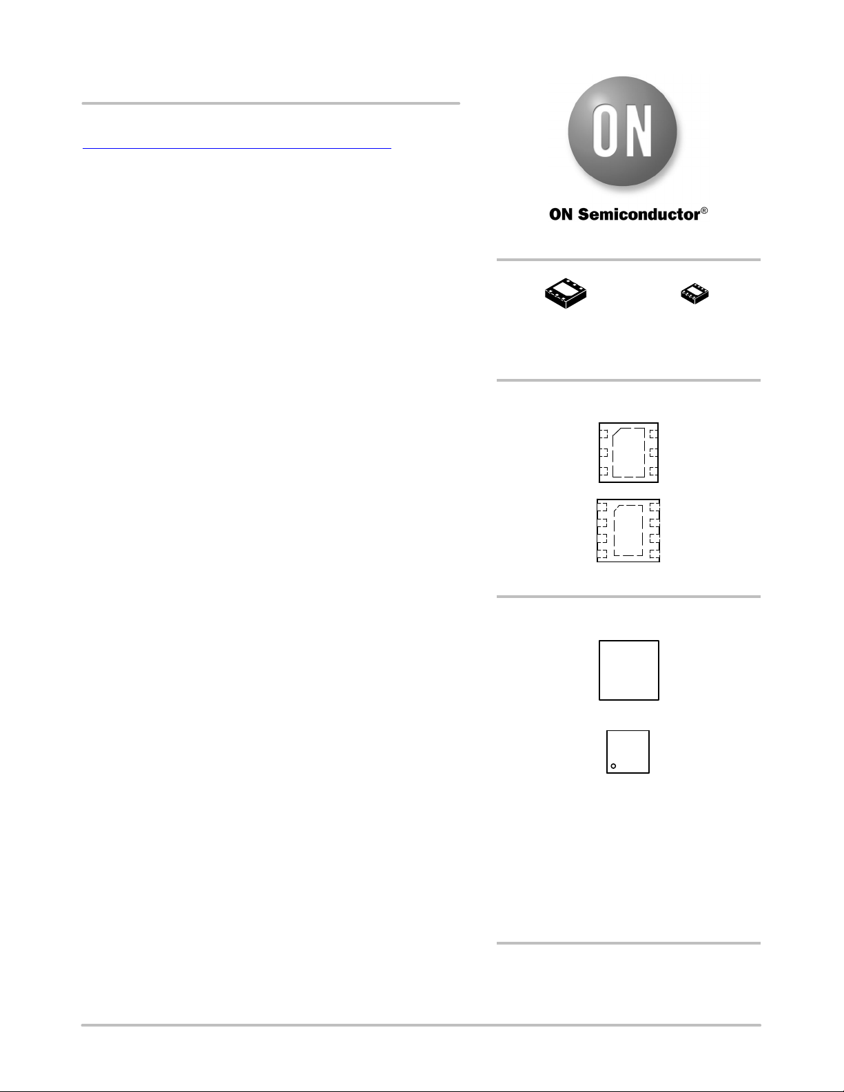
http://onsemi.com
1
WDFN−6
3 x 3 mm
CASE 511AP
PIN CONNECTIONS
1
EN
GND
BYP
1
VIN
VIN
GND ADJ
(Top Views)
MARKING DIAGRAMS
62XX
LAAA
YWW
G
1
XXL
YM
G
1
XX = Specific Device Code
62XX = Specific Device Code
L = Assembly Location Code
AAA = Assembly Lot Number
Y = Production Year (Last Digit)
M = Production Month (1−9, O, N, D)
WW = Production Week (Two Digits)
G = Pb−Free Package
= (Last Three Digits)
UDFN−8
2 x 2 mm
CASE 517AW
VIN
ADJ
VOUT
VOUT
VOUT
BYPEN
(WDFN−6)
(UDFN−8)
© Semiconductor Components Industries, LLC, 2013
September, 2019 − Rev. 6
ORDERING INFORMATION
See detailed ordering and shipping information in the package
dimensions section on page 17 of this data sheet.
1 Publication Order Number:
CAT6241/D
Page 2
CAT6241
VIN
VIN
VIN
EN
VIN
VOUT
ENABLE
C
IN
1 mF
CAT6241
ADJBYP
C
BYP
GND
(Optional)
Figure 1. Application Schematic
I
SENSE
Thermal
Shutdown
Enable
Logic
2.5 M
+
−
+
−
V
REF
C
OUT
2.2 mF
VOUT
VOUT
ADJ
BYP
VOUT
GND
Figure 2. Simplified Block Diagram
Table 1. PIN FUNCTION DESCRIPTION
Pin #
WDFN−6
1 4 EN The Enable Input. An active HIGH input, turning ON the LDO. This input should be tied to
2, PAD 3, PAD GND Power Supply Ground; Device Substrate. The center pad is internally connected to Ground
3 5 BYP Bypass input. Placing a capacitor of 100 pF to 470 pF between BYP and ground reduces
4 7, 8 V
5 6 ADJ Output Voltage Adjust Input. This input ties to the common point of a resistor divider which
6 1, 2 V
Pin #
UDFN−8
Pin Name Description
if the LDO is not intended to be shut off during normal operation. A pull−down 2.5 MW
V
IN
resistor maintains the circuit in the OFF state if the pin is left open.
and as such can cause short circuits to signal traces running beneath the IC. This pad is
intended for heat sinking the IC to the PCB and is typically connected to the PCB ground
plane.
OUT
noise on V
Regulated Output Voltage. A protection block eliminates any current flow from output to
input if V
This capacitor is optional.
OUT.
> VIN. Connect both pins for specified dropout performance.
OUT
determines the regulator’s output voltage. See Applications section for details on selecting
resistor values.
IN
Positive Power Supply Input. Supplies power for V
circuitry. Connect both pins for specified dropout performance.
as well as the regulator’s internal
OUT
http://onsemi.com
2
Page 3
CAT6241
Table 2. ABSOLUTE MAXIMUM RATINGS
Rating Symbol Value Unit
Input Voltage Range (Note 1) V
Output Voltage Range V
IN
OUT
Enable Input Range EN −0.3 to 5.5 V or (VIN + 0.3),
Adjust Input Range ADJ −0.3 to 5.5 V V
Bypass Input Range BYP −0.3 to 5.5 V or (VIN + 0.3),
Power Dissipation
Maximum Junction Temperature T
Storage Temperature Range T
ESD Capability, Human Body Model (Note 2) ESD
ESD Capability, Machine Model (Note 2) ESD
Lead Temperature Soldering
Reflow (SMD Styles Only), Pb−Free Versions (Note 3)
PD
J(max)
STG
HBM
T
SLD
MM
Stresses exceeding Maximum Ratings may damage the device. Maximum Ratings are stress ratings only. Functional operation above the
Recommended Operating Conditions is not implied. Extended exposure to stresses above the Recommended Operating Conditions may affect
device reliability.
1. Refer to ELECTRICAL CHARACTERISTIS and APPLICATION INFORMATION for Safe Operating range.
2. This device series incorporates ESD protection and is tested by the following methods:
ESD Human Body Model tested per AEC−Q100−002 (EIA/JESD22−A114)
ESD Machine Model tested per AEC−Q100−003 (EIA/JESD22−A115)
Latchup Current Maximum Rating: ≤150 mA per JEDEC standard: JESD78
3. For information, please refer to our Soldering and Mounting Techniques Reference Manual, SOLDERRM/D
−0.3 to 6.0 V
−0.3 to 6.0 V
V
whichever is lower
V
whichever is lower
Internally Limited mW
150 °C
−65 to 150 °C
2 kV
200 V
260 °C
Table 3. THERMAL CHARACTERISTICS
Rating Symbol Value Unit
Thermal Characteristics, WDFN−6, 3 x 3 mm
Thermal Resistance, Junction−to−Air: 1 in
Thermal Reference, Junction−to−Case (Note 4)
2
/1 oz. copper (Note 4)
R
q
JA
R
y
JL
4. Values based on copper area of 645 mm2 (or 1 in2) of 1 oz copper thickness and FR4 PCB substrate.
Table 4. OPERATING RANGES (Note 5)
Rating
Input Voltage (Note 6) V
Output Current I
Output Voltage V
Ambient Temperature T
5. Refer to ELECTRICAL CHARACTERISTIS and APPLICATION INFORMATION for Safe Operating range.
6. Minimum V
IN_MIN
= 1.6 V or (V
Table 5. ELECTRICAL CHARACTERISTICS (V
typical values T
Symbol
= 25°C, for Bold values TA = −40°C to 85°C; unless otherwise noted.)
A
+ VDO), whichever is higher.
OUT
IN
= (V
+ 1 V) or V
OUT
Parameter Conditions Min Typ Max Unit
INPUT / OUTPUT
V
V
OUT
V
OUT−ACC
V
ADJ
TC
OUT
I
OUT
IN
Input Voltage 1.6 5.5 V
Output Voltage Range 0.5 5.0 V
Output Voltage Accuracy Initial accuracy, I
Voltage at ADJ input 0.485 0.5 0.515 V
Output Voltage Temp. Coefficient 50 ppm/°C
Output Current 0.0001 1 A
Symbol Min Max Unit
IN
OUT
OUT
A
, whichever is higher, CIN = 1 mF, C
IN_MIN
= 1 mA
OUT
1.6 5.5 V
0.1 1000 mA
0.5 5.0 V
−40 85 °C
−2 2
−3 3
55
10
= 2.2 mF, for
OUT
°C/W
%
http://onsemi.com
3
Page 4
CAT6241
Table 5. ELECTRICAL CHARACTERISTICS (V
typical values T
= 25°C, for Bold values TA = −40°C to 85°C; unless otherwise noted.)
A
IN
= (V
+ 1 V) or V
OUT
, whichever is higher, CIN = 1 mF, C
IN_MIN
= 2.2 mF, for
OUT
Symbol UnitMaxTypMinConditionsParameter
INPUT / OUTPUT
V
R−LINE
V
R−LOAD
V
DO
I
ADJ
I
GND
I
GND−SD
ISC Output short circuit current limit V
Line Regulation
Load Regulation
V
≥ 0.8 V
OUT
V
= 1.2 V
OUT
V
= 2.5 V 11 0
OUT
V
= 3.3 V 85
OUT
V
= 1.2 V
OUT
V
= 2.5 V 350
OUT
V
= 3.3 V 275
OUT
VIN = V
I
OUT
VIN = V
I
OUT
I
OUT
I
OUT
I
OUT
T
= 25°C
A
I
OUT
T
= 25°C
A
+ 1.0 V to 5.5 V,
OUT
= 10 mA
+ 1.0 V to 5.5 V,
OUT
= 10 mA
= 100 mA to 1000 mA
= 100 mA to 1000 mA
= 300 mA
= 1 A
−0.3 ±0.08 0.3
−0.45 0.45
1.5 2
3
460
700
%/V
%
mV
ADJ Input Current 100 nA
Ground Current
I
= 0 mA
OUT
I
= 0 mA
OUT
I
= 1000 mA 140 200
OUT
I
= 1000 mA 250
OUT
70
100
Shutdown Ground Current VEN < 0.4 V 5
= 0 V 900 mA
OUT
mA
mA
PSRR AND NOISE
PSRR
e
N
UVLO, R
V
UVLO
R
OUT−SH
ESR C
Power Supply Rejection Ratio
Output Noise Voltage for 1.2 V output BW = 10 Hz to 100 kHz
AND ESR
OUT
f = 1 kHz, BYP = 470 pF,
I
= 10 mA
OUT
f = 20 kHz, BYP = 470 pF,
I
= 10 mA
OUT
BYP = 470 pF, I
OUT
= 10 mA
54
42
45
Under voltage lockout threshold 1.4 1.55 V
ON resistance of Discharge Transistor 150
equivalent series resistance 5 500
OUT
dB
mVrms
W
mW
ENABLE INPUT
V
HI
V
LO
I
EN
Logic High Level VIN = 1.6 to 5.5 V 1.6 V
Logic Low Level VIN = 1.6 to 5.5 V 0.4 V
Enable Input Current
VEN = 0.4 V 0.15 1
mA
VEN = VIN = 2.5 V 1 3
R
EN
Enable pull−down resistor 2.5
MW
TIMING
T
ON
Turn−On Time
C
= 0 pF 230
BYP
C
= 470 pF 1600
BYP
ms
THERMAL PROTECTION
T
SD
T
HYS
Thermal Shutdown 145 °C
Thermal Hysteresis 10 °C
7. Performance guaranteed over the indicated operating temperature range by design and/or characterization tested at TJ = TA = 25_C. Low
duty cycle pulse techniques are used during testing to maintain the junction temperature as close to ambient as possible.
8. Output current capability depends upon the value of both V
Figure 13). For V
> 0.8 V, current capability is 1 A for VIN ≥ 1.8 V.
OUT
and V
IN
OUT
. For V
≤ 0.8 V, output current capability is 90% of ISC (see
OUT
http://onsemi.com
4
Page 5
(shown for V
ADJ
= V
= 0.5 V, VIN = 1.6 V, I
OUT
CAT6241
TYPICAL CHARACTERISTICS
= 1 mA, CIN = 1 mF, C
OUT
= 4.7 mF, C
OUT
= 0, and TA = 25°C unless otherwise specified.)
BYP
600
500
400
300
200
OUTPUT VOLTAGE (mV)
100
0
530
520
510
500
490
OUTPUT VOLTAGE (mV)
480
470
510
1 mA
400 mA
2.5 5.5
INPUT VOLTAGE (V)
3.5
5.0
4.54.03.02.01.51.00.50
505
500
495
OUTPUT VOLTAGE (mV)
490
1.51.00.5
INPUT VOLTAGE (V)
Figure 3. Dropout Characteristics Figure 4. Line Regulation
550
500
450
400
350
300
250
200
150
OUTPUT VOLTAGE (mV)
100
50
400
OUTPUT LOAD CURRENT (mA) OUTPUT LOAD CURRENT (mA)
5003002001000
0
200 400 500 600
3001000
Figure 5. Load Regulation Figure 6. Output Current Capability
5.5
5.04.54.03.53.02.52.00
100
90
80
70
60
50
40
GROUND CURRENT (mA)
30
20
OUTPUT LOAD CURRENT (mA) INPUT VOLTAGE (V)
5004003002001000
100
90
80
70
60
50
40
30
20
GROUND CURRENT (mA)
10
0
1.0 2.0 3.5 5.5
4.54.03.02.51.50.50
5.0
Figure 7. Ground Current vs. Load Current Figure 8. Ground Current vs. Input Voltage
http://onsemi.com
5
Page 6

(shown for V
ADJ
= V
= 0.5 V, VIN = 1.6 V, I
OUT
CAT6241
TYPICAL CHARACTERISTICS
= 1 mA, CIN = 1 mF, C
OUT
= 4.7 mF, C
OUT
= 0, and TA = 25°C unless otherwise specified.)
BYP
520
515
510
505
500
495
490
OUTPUT VOLTAGE (mV)
485
480
1.2
1.0
0.8
0.6
80
70
60
50
40
30
20
GROUND CURRENT (mA)
10
40 120
TEMPERATURE (°C)
80
10060200−20−40
0
10060200−20−40 40 12080
TEMPERATURE (°C)
Figure 9. Output Voltage vs. Temperature Figure 10. Ground Current vs. Temperature
1.2
1.0
0.8
0.6
0.4
0.2
RISING ENABLE THRESHOLD (V)
0
3.0 4.5 5.5
INPUT VOLTAGE (V) INPUT VOLTAGE (V)
Figure 11. Rising Enable Threshold vs. Input
Voltage
1400
1200
1000
SHORT CIRCUIT CURRENT (mA)
0.4
0.2
FALLING ENABLE THRESHOLD (V)
5.04.03.52.52.01.5
800
600
400
200
0
INPUT VOLTAGE (V)
0
V
= 0
OUT
35
Figure 13. Output Short−circuit Current vs.
Input Voltage
3.0 4.5 5.5
5.04.03.52.52.01.5
Figure 12. Falling Enable Threshold vs. Input
Voltage
4210
http://onsemi.com
6
Page 7

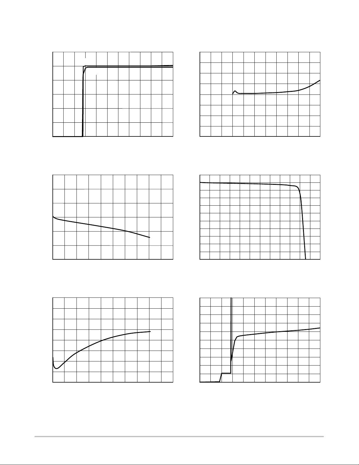
CAT6241
TRANSIENT CHARACTERISTICS
(shown for V
Figure 14. Enable Turn−on (1 mA Load) Figure 15. Enable Turn−off (1 mA Load)
= 0.5 V, VIN = 1.6 V, I
OUT
= 1 mA, CIN = 1 mF, C
OUT
= 4.7 mF, C
OUT
= 0, and TA = 25°C unless otherwise specified.)
BYP
Figure 16. Enable Turn−on (350 mA Load) Figure 17. Enable Turn−off (350 mA Load)
Figure 18. Enable Turn−on (1 mA Load)
C
= 470 pF
BYP
Figure 19. Enable Turn−on (350 mA Load)
C
= 470 pF
BYP
http://onsemi.com
7
Page 8

(shown for V
= 0.5 V, VIN = 1.6 V, I
OUT
CAT6241
TRANSIENT CHARACTERISTICS
= 1 mA, CIN = 1 mF, C
OUT
= 4.7 mF, C
OUT
= 0, and TA = 25°C unless otherwise specified.)
BYP
Figure 20. Load Transient Response
(1 mA to 350 mA)
Figure 22. Load Transient Response
(1 mA to 500 mA) V
= 1.9 V
IN
Figure 21. Load Transient Response
(1 mA to 500 mA) V
= 1.8 V
IN
Figure 23. Load Transient Response
(1 mA to 500 mA) VIN = 2.0 V
http://onsemi.com
8
Page 9

(shown for V
= 1.0 V, VIN = 2.0 V, I
OUT
CAT6241
TYPICAL CHARACTERISTICS
= 1 mA, CIN = 1 mF, C
OUT
= 4.7 mF, C
OUT
= 0, and TA = 25°C unless otherwise specified.)
BYP
1100
1000
900
800
700
600
500
400
300
OUTPUT VOLTAGE (V)
200
100
0
1040
1030
1020
1010
1000
990
980
970
OUTPUT VOLTAGE (mV)
960
950
940
1010
RL = 1 KW
RL = 1 W
1005
RL = 2 W
1000
995
OUTPUT VOLTAGE (mV)
2.0 5.0
2.5 3.5 5.5
INPUT VOLTAGE (V)
4.0
4.53.01.51.00.50
990
INPUT VOLTAGE (V)
Figure 24. Dropout Characteristics Figure 25. Line Regulation
1100
1000
900
800
700
600
500
400
300
OUTPUT VOLTAGE (mV)
200
100
300 600 1000
OUTPUT LOAD CURRENT (mA) OUTPUT LOAD CURRENT (mA)
700 900
8005004002001000
0
Figure 26. Load Regulation Figure 27. Output Current Capability
4.53.01.51.00.50 2.0 5.04.02.5 3.5 5.5
12008006004002000
1000 1400
100
90
80
70
60
50
40
GROUND CURRENT (mA)
30
20
OUTPUT LOAD CURRENT (mA)
600 1000
8004002000
Figure 28. Ground Current vs. Load Current
http://onsemi.com
9
Page 10

CAT6241
TRANSIENT CHARACTERISTICS
(shown for V
= 1.0 V, VIN = 2.0 V, I
OUT
= 1 mA, CIN = 1 mF, C
OUT
= 4.7 mF, C
OUT
= 0, and TA = 25°C unless otherwise specified.)
BYP
Figure 29. Enable Turn−on (1 mA Load) Figure 30. Enable Turn−off (1 mA Load)
Figure 31. Enable Turn−on (1 A Load) Figure 32. Enable Turn−off (1 A Load)
Figure 33. Enable Turn−on (1 mA Load)
C
= 470 pF
BYP
Figure 34. Enable Turn−on (1 A Load)
C
= 470 pF
BYP
http://onsemi.com
10
Page 11

(shown for V
= 1.0 V, VIN = 2.0 V, I
OUT
CAT6241
TRANSIENT CHARACTERISTICS
= 1 mA, CIN = 1 mF, C
OUT
= 4.7 mF, C
OUT
= 0, and TA = 25°C unless otherwise specified.)
BYP
Figure 35. Load Transient Response
(1 mA to 1 A)
Figure 36. Load Transient Response
(1 mA to 1 A) V
= 2.2 V
IN
http://onsemi.com
11
Page 12

CAT6241
PIN FUNCTIONS
V
IN
Positive Power Input. Power is supplied to the device
through the V
pin. A bypass capacitor is required on this
IN
pin if the device is more than six inches away from the main
input filter capacitor. In general it is advisable to include a
small bypass capacitor adjacent to the regulator. In
battery−powered circuits this is particularly important
because the output impedance of a battery rises with
frequency, so a bypass capacitor in the range of 1 mF to 10 mF
is recommended.
GND
Ground. The negative voltage of the input power source.
The center pad on the back of the package is also electrically
ground. This pad is used for cooling the device by making
connection to the buried ground plane through solder filled
vias or by contact with a topside copper surface exposed to
free flowing air.
ENABLE
ENABLE is an active high logic input which controls the
regulator’s the output state. If ENABLE < 0.4 V the
regulator is shutdown and V
= 0 V. If ENABLE > 1.6 V
OUT
the regulator is active and supplying power to the load.
If the regulator is intended to operate continuously and
won’t be shut down from time to time ENABLE should be
tied to V
BYP
IN
.
The Bypass Capacitor input is used to decrease output
voltage noise by placing a capacitor between BYP and
ground. The recommended range of capacitance is from
100 pF to 470 pF. Values larger than this will provide no
additional improvement and will further extend CAT6241’s
startup time.
A bypass capacitor is not required for operation and BYP
may be left open or floating if no capacitor is used but DO
NOT ground BYP as this will interfere with the error
amplifier’s functioning.
ADJ
ADJ = Adjust and is the voltage control input. ADJ
connects to the center point of a resistor divider which
determines the CAT6241’s output voltage. See Applications
Section for resistor selection guidelines.
V
OUT
V
is the regulator’s output and supplies power to the
OUT
load. V
can be shut off via the ENABLE input. All
OUT
CAT6241 members are designed to block reverse current,
meaning anytime V
becomes greater than VIN the pass
OUT
FET will be shut off so there is no reverse current flow from
output to input. CAT6241 is also equipped with an output
discharge transistor that is turned ON anytime ENABLE is
at a logic Low. This transistor ensures V
discharges to
OUT
0 V when the regulator is shutdown. This is especially
important when powering digital circuitry because if V
OUT
fails to reach 0 V their POR (power−ON reset) circuitry may
not trigger and scrambled data or unpredictable operations
may result.
A minimum output capacitor of 2.2 mF should be placed
between V
Increasing the size of C
and GND to insure stable operation.
OUT
, up to 22 mF, will improve
OUT
transient response to large changes in load current.
http://onsemi.com
12
Page 13

CAT6241
APPLICATIONS INFORMATION
Input Decoupling (CIN)
A ceramic or tantalum 1 mF capacitor is recommended and
should be connected close to the CAT6241’s package.
Higher capacitance and lower ESR will improve the overall
line and load transient response.
Output Decoupling (C
OUT
)
The minimum output decoupling value is 2.2 mF and can
be augmented to fulfill stringent load transient
requirements. Larger values, up to 22 mF, improve noise
rejection and load regulation transient response. The
CAT6241 is a highly stable regulator and performs well over
a wide range of Equivalent Series Resistances (ESR) with
ceramic chip capacitors.
No−Load Regulation Considerations
The CAT6241 adjustable regulator will operate properly
under conditions where the only load current is through the
resistor divider that sets the output voltage. However, in the
case where the CAT6241 is configured to provide a 0.5 V
output, there is no resistor divider and the ADJ pin is
connected to VOUT. If the part is enabled under no−load
conditions, leakage current through the pass transistor at
junction temperatures above 85°C can approach several
microamperes, especially as junction temperature
approaches 150°C. If this leakage current is not directed into
a load, the output voltage will rise above nominal until a load
is applied. For this reason it is recommended that a minimum
load of 100 mA be present at all times. Normally the voltage
setting resistor divider will serve this function but if no
divider is used (VOUT = 0.5 V) then an external load of
5KW should be provided.
Output Voltage Adjust
The output voltage can be adjusted from 0.5 V to 5.0 V
using resistors between the output and the ADJ input. The
output voltage and resistors are chosen using Equation 1 and
Equation 2.
R
V
+ 0.5ǒ1 )
OUT
R2^
R1^ R
0.5 V
I
DIV
ǒ
2
V
OUT
0.5 V
R
* 1
1
Ǔ
)ǒI
ADJ
2
Ǔ
R
Ǔ
1
(eq. 1)
(eq. 2)
(eq. 3)
VIN VOUT
C
IN
Figure 37. Adjustable Output Resistor Divider
VIN
ENABLE
BYP
C
BYP
Input bias current, I
ignored (I
recommended I
load on V
= 0). Considering that the lowest
ADJ
value is 100 mA, then, when there is no
OUT
, I
OUT
divider
VOUT
R
CAT6241
ADJ
GND
, for all practical designs can be
ADJ
1
C
OUT
R
2
must be 100 mA to keep CAT6241 in
regulation. This then sets R2’s value using Equation 2 to
5KW, which minimizes output noise. Use Equation 3 to find
the required value for R1. If needed, lower values for IDIV
can be considered, but not lower than 10 mA. The trade−off
will be worse values for both load regulation and TCOUT.
Thermal Considerations
As power in the CAT6241 increases, it may become
necessary to provide thermal relief. The maximum power
dissipation supported by this device is dependent upon
board design and layout. Mounting pad configuration on the
PCB, the board material, and the ambient temperature affect
the rate of junction temperature rise for the part. When the
CAT6241 has good thermal conductivity through the PCB,
the junction temperature will be relatively low even with
high power applications. The maximum dissipation the
CAT6241 can handle is given by:
P
D(MAX)
+
ƪ
T
J(MAX)
R
qJA
* T
ƫ
A
(eq. 4)
Since TJ is not recommended to exceed 125°C, then with
CAT6241 soldered to 645 mm
2
(1 sq inch), 1 oz copper area,
FR4 PCB material can dissipate in excess of 1 W when the
ambient temperature (T
) is 25°C. Note that this assumes the
A
pad in the center of the package is soldered to the dissipating
copper foil. See Figure below for R
heat dissipating areas smaller than 645 mm
versus PCB area for
JA
q
2
. Power
dissipation can be calculated from the following equations:
PD[ VIN(I
GND
) I
OUT
) ) I
OUT
(VIN* V
OUT
)
(eq. 5)
or
V
IN(MAX)
P
[
D(MAX)
I
OUT
) (V
) I
OUT
GND
I
OUT
)
(eq. 6)
http://onsemi.com
13
Page 14

300
CAT6241
250
200
150
Theta JA (°C/W)
100
50
0
0 25 50 75 100 125 150 175 200 225 250 275 300 650
Copper heat spreading area (mm
1 oz C.F
2 oz C.F
1 oz Sim
2 oz Sim
2
)
Figure 38. Thermal Resistance vs. PCB Copper Area for 3 mm x 3 mm WDFN Package
PCB Layout Top Layer and
connections to heat spreading plane
Close−up of pad area
Figure 39. Topside Copper Foil Pattern for Heat Dissipation
Design Hints
VIN and GND printed circuit board traces should be as
wide as possible. When the impedance of these traces is high
due to narrow trace width or long length, there is a chance
to pick up noise or cause the regulator to malfunction. Place
http://onsemi.com
external components, especially the input and output
capacitors, as close as possible to the CAT6241, and keep
traces between power source and load as short as possible.
14
Page 15

MECHANICAL CASE OUTLINE
PACKAGE DIMENSIONS
1
SCALE 2:1
B
DETAIL B
A1
4
5
1.73
8X
A
E
A
8X
E2
b
0.10 C
0.05 C
A3
SEATING
C
PLANE
L
A
NOTE 3
8X
0.50
PIN ONE
REFERENCE
2X
2X
NOTE 4
DETAIL A
D
C0.10
C0.10
TOP VIEW
C0.10
C0.08
SIDE VIEW
D2
1
8
e
e/2
BOTTOM VIEW
RECOMMENDED
SOLDERING FOOTPRINT*
PACKAGE
OUTLINE
L1
BB
UDFN8, 2x2
CASE 517AW
ISSUE A
L
DETAIL A
ALTERNATE
CONSTRUCTIONS
EXPOSED Cu
A1
DETAIL B
ALTERNATE
CONSTRUCTION
MOLD CMPD
A3
DATE 13 NOV 2015
L
NOTES:
1. DIMENSIONING AND TOLERANCING PER
ASME Y14.5M, 1994.
2. CONTROLLING DIMENSION: MILLIMETERS.
3. DIMENSION b APPLIES TO PLATED TERMINALS AND IS MEASURED BETWEEN 0.15
AND 0.30 MM FROM THE TERMINAL TIP.
4. COPLANARITY APPLIES TO THE EXPOSED
PAD AS WELL AS THE TERMINALS.
5. FOR DEVICE OPN CONTAINING W OPTION,
DETAIL B ALTERNATE CONSTRUCTION IS
NOT APPLICABLE.
MILLIMETERS
DIM MIN MAX
A 0.45 0.55
A1 0.00 0.05
A3 0.13 REF
b 0.18 0.30
D 2.00 BSC
D2 1.50 1.70
E 2.00 BSC
E2 0.80 1.00
e 0.50 BSC
L 0.20 0.45
L1 −−− 0.15
GENERIC
MARKING DIAGRAM*
1
XX MG
G
XX = Specific Device Code
M = Date Code
G = Pb−Free Package
(Note: Microdot may be in either location)
*This information is generic. Please refer to
device data sheet for actual part marking.
Pb−Free indicator, “G” or microdot “ G”,
may or may not be present.
8X
0.30
2.30
1.00
0.50
PITCH
1
DIMENSIONS: MILLIMETERS
*For additional information on our Pb−Free strategy and soldering
details, please download the ON Semiconductor Soldering and
Mounting Techniques Reference Manual, SOLDERRM/D.
DOCUMENT NUMBER:
DESCRIPTION:
ON Semiconductor and are trademarks of Semiconductor Components Industries, LLC dba ON Semiconductor or its subsidiaries in the United States and/or other countries.
ON Semiconductor reserves the right to make changes without further notice to any products herein. ON Semiconductor makes no warranty, representation or guarantee regarding
the suitability of its products for any particular purpose, nor does ON Semiconductor assume any liability arising out of the application or use of any product or circuit, and specifically
disclaims any and all liability, including without limitation special, consequential or incidental damages. ON Semiconductor does not convey any license under its patent rights nor the
rights of others.
© Semiconductor Components Industries, LLC, 2019
98AON34462E
UDFN8, 2X2
Electronic versions are uncontrolled except when accessed directly from the Document Repository.
Printed versions are uncontrolled except when stamped “CONTROLLED COPY” in red.
PAGE 1 OF 1
www.onsemi.com
Page 16

ON Semiconductor and are trademarks of Semiconductor Components Industries, LLC dba ON Semiconductor or its subsidiaries in the United States and/or other countries.
ON Semiconductor owns the rights to a number of patents, trademarks, copyrights, trade secrets, and other intellectual property. A listing of ON Semiconductor’s product/patent
coverage may be accessed at www.onsemi.com/site/pdf/Patent−Marking.pdf
ON Semiconductor makes no warranty, representation or guarantee regarding the suitability of its products for any particular purpose, nor does ON Semiconductor assume any liability
arising out of the application or use of any product or circuit, and specifically disclaims any and all liability, including without limitation special, consequential or incidental damages.
Buyer is responsible for its products and applications using ON Semiconductor products, including compliance with all laws, regulations and safety requirements or standards,
regardless of any support or applications information provided by ON Semiconductor. “Typical” parameters which may be provided in ON Semiconductor data sheets and/or
specifications can and do vary in different applications and actual performance may vary over time. All operating parameters, including “Typicals” must be validated for each customer
application by customer’s technical experts. ON Semiconductor does not convey any license under its patent rights nor the rights of others. ON Semiconductor products are not
designed, intended, or authorized for use as a critical component in life support systems or any FDA Class 3 medical devices or medical devices with a same or similar classification
in a foreign jurisdiction or any devices intended for implantation in the human body. Should Buyer purchase or use ON Semiconductor products for any such unintended or unauthorized
application, Buyer shall indemnify and hold ON Semiconductor and its officers, employees, subsidiaries, affiliates, and distributors harmless against all claims, costs, damages, and
expenses, and reasonable attorney fees arising out of, directly or indirectly, any claim of personal injury or death associated with such unintended or unauthorized use, even if such
claim alleges that ON Semiconductor was negligent regarding the design or manufacture of the part. ON Semiconductor is an Equal Opportunity/Affirmative Action Employer. This
literature is subject to all applicable copyright laws and is not for resale in any manner.
. ON Semiconductor reserves the right to make changes without further notice to any products herein.
PUBLICATION ORDERING INFORMATION
LITERATURE FULFILLMENT:
Email Requests to: orderlit@onsemi.com
ON Semiconductor Website: www.onsemi.com
TECHNICAL SUPPORT
North American Technical Support:
Voice Mail: 1 800−282−9855 Toll Free USA/Canada
Phone: 011 421 33 790 2910
Europe, Middle East and Africa Technical Support:
Phone: 00421 33 790 2910
For additional information, please contact your local Sales Representative
◊
www.onsemi.com
1
 Loading...