

Page 1
EEPROM Serial 512-Kb SPI
CAT25512
Description
The CAT25512 is a EEPROM Serial 512−Kb SPI device internally
organized as 64Kx8 bits. This features a 128−byte page write buffer
and supports the Serial Peripheral Interface (SPI) protocol. The device
is enabled through a Chip Select (CS) input. In addition, the required
bus signals are clock input (SCK), data input (SI) and data output (SO)
lines. The HOLD
communication with the CAT25512 device. The device features
software and hardware write protection, including partial as well as
full array protection.
On−Chip ECC (Error Correction Code) makes the device suitable
for high reliability applications.
Features
• 20 MHz SPI Compatible
• 1.8 V to 5.5 V Supply Voltage Range
• SPI Modes (0,0) & (1,1)
• 128−byte Page Write Buffer
• Additional Identification Page with Permanent Write Protection
• Self−timed Write Cycle
• Hardware and Software Protection
• Block Write Protection
1
− Protect
/4, 1/2 or Entire EEPROM Array
• Low Power CMOS Technology
• 1,000,000 Program/Erase Cycles
• 100 Year Data Retention
• Industrial and Extended Temperature Range
• SOIC, TSSOP 8−lead, UDFN 8−pad
• This Device is Pb−Free, Halogen Free/BFR Free, and RoHS
Compliant
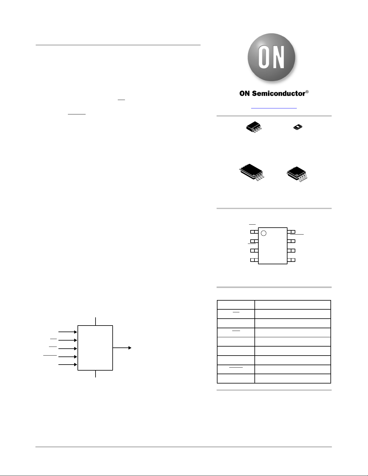
SI
CS
WP
HOLD
SCK
Figure 1. Functional Symbol
input may be used to pause any serial
V
CC
CAT25512
V
SS
SO
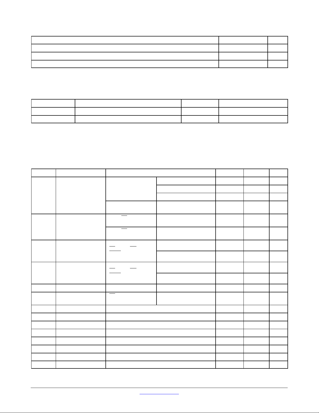
www.onsemi.com
SOIC−8
V SUFFIX
CASE 751BD
TSSOP−8
Y SUFFIX
CASE 948AL
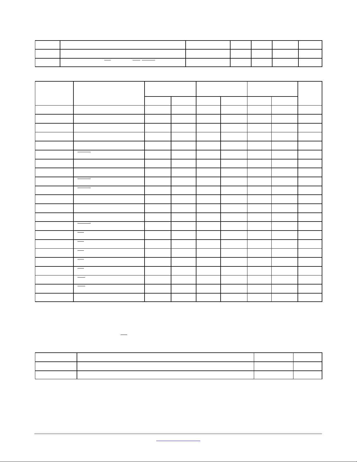
PIN CONFIGURATIONS
CS
SO
WP
V
SOIC (V, X), TSSOP (Y), UDFN (HU5)
SS
CC
ORDERING INFORMATION
See detailed ordering and shipping information in the package
dimensions section on page 11 of this data sheet.
1
SS
(Top View)
PIN FUNCTION
Chip SelectCS
Serial Data OutputSO
Write ProtectWP
GroundV
Serial Data InputSI
Serial ClockSCK
Hold Transmission InputHOLD
Power SupplyV
UDFN−8
HU5 SUFFIX
CASE 517BU
SOIC−8 WIDE
X SUFFIX
CASE 751BE
V
CC
HOLD
SCK
SI
FunctionPin Name
© Semiconductor Components Industries, LLC, 2016
December, 2020 − Rev. 11
1 Publication Order Number:
CAT25512/D
Page 2
CAT25512
Table 1. ABSOLUTE MAXIMUM RATINGS
Parameters Ratings Units
Operating Temperature −45 to +130 °C
Storage Temperature −65 to +150 °C
Voltage on any Pin with Respect to Ground (Note 1) −0.5 to +6.5 V
Stresses exceeding those listed in the Maximum Ratings table may damage the device. If any of these limits are exceeded, device functionality
should not be assumed, damage may occur and reliability may be affected.
1. The DC input voltage on any pin should not be lower than −0.5 V or higher than V
undershoot to no less than −1.5 V or overshoot to no more than V
+ 1.5 V, for periods of less than 20 ns.
CC
Table 2. RELIABILITY CHARACTERISTICS (Note 2)
Symbol
N
(Note 3, 4) Endurance 1,000,000 Program / Erase Cycles
END
T
DR
Data Retention 100 Years
2. These parameters are tested initially and after a design or process change that affects the parameter according to appropriate AEC−Q100
and JEDEC test methods.
3. Write Mode: groups of 4 bytes, 25°C.
4. The device uses ECC (Error Correction Code) logic with 6 ECC bits to correct one bit error in 4 data bytes. Therefore, when a single byte
has to be written, 4 bytes (including the ECC bits) are re−programmed. It is recommended to write by multiple of 4 bytes in order to benefit
from the maximum number of write cycles.
Parameter Max Units
Table 3. D. C. OPERATING CHARACTERISTICS
(VCC = 1.8 V to 5.5 V, TA = −40°C to +85°C and VCC = 2.5 V to 5.5 V, TA = −40°C to +125°C, unless otherwise specified)
Symbol
I
CCR
I
CCW
I
SB1
I
SB2
I
L
I
LO
V
IL1
V
IH1
V
IL2
V
IH2
V
OL1
V
OH1
V
OL2
V
OH2
Product parametric performance is indicated in the Electrical Characteristics for the listed test conditions, unless otherwise noted. Product
performance may not be indicated by the Electrical Characteristics if operated under different conditions.
Parameter Test Conditions Min Max Units
Supply Current
(Read Mode)
Read, SO open /
−40°C to +85°C
VCC = 1.8 V, f
V
= 2.5 V, f
CC
VCC = 5.5 V, f
Supply Current
(Write Mode)
Read, SO open /
−40°C to +125°C
Write, CS = VCC/
−40°C to +85°C
Write, CS = VCC/
2.5 V < VCC < 5.5 V,
f
SCK
1.8 V < VCC < 5.5 V 2 mA
2.5 V < VCC < 5.5 V 2 mA
−40°C to +125°C
Standby Current VIN = GND or VCC,
CS
= VCC, WP = VCC,
HOLD = VCC,
VCC = 5.5 V
Standby Current VIN = GND or VCC,
TA = −40°C to +85°C 1
TA = −40°C to +125°C 3
TA = −40°C to +85°C 3
CS = VCC, WP = GND,
HOLD = GND,
VCC = 5.5 V
Input Leakage Current VIN = GND or V
Output Leakage
Current
CS = V
V
OUT
CC
= GND or V
CC
CC
TA = −40°C to +125°C 5
Input Low Voltage VCC ≥ 2.5 V −0.5 0.3V
Input High Voltage VCC ≥ 2.5 V 0.7V
Input Low Voltage VCC < 2.5 V −0.5 0.25V
Input High Voltage VCC < 2.5 V 0.75V
Output Low Voltage VCC ≥ 2.5 V, IOL = 3.0 mA 0.4 V
Output High Voltage VCC ≥ 2.5 V, IOH = −1.6 mA VCC − 0.8V V
Output Low Voltage
Output High Voltage
VCC < 2.5 V, IOL = 150 mA
VCC < 2.5 V, IOH = −100 mA
+ 0.5 V. During transitions, the voltage on any pin may
CC
= 5 MHz 1.2 mA
SCK
= 10 MHz 1.8 mA
SCK
= 20 MHz 3 mA
SCK
3 mA
= 10 MHz
−2 2
−2 2
CC
CC
VCC + 0.5 V
CC
VCC + 0.5 V
CC
0.2 V
VCC − 0.2V V
mA
mA
mA
mA
mA
V
V
www.onsemi.com
2
Page 3
CAT25512
Table 4. PIN CAPACITANCE (T
Symbol
C
OUT
C
IN
Output Capacitance (SO) V
Input Capacitance (CS, SCK, SI, WP, HOLD) VIN = 0 V 8 pF
Table 5. A.C. CHARACTERISTICS (T
Symbol
f
SCK
t
t
t
t
SU
t
WH
WL
LZ
H
Clock Frequency DC 5 DC 10 DC 20 MHz
Data Setup Time 20 10 5 ns
Data Hold Time 20 10 5 ns
SCK High Time 75 40 20 ns
SCK Low Time 75 40 20 ns
HOLD to Output Low Z 50 25 25 ns
= 25°C, f = 1.0 MHz, VCC = +5.0 V) (Note 2)
A
Test Conditions Min Typ Max Units
= −40°C to +125°C, unless otherwise specified.) (Note 5)
A
VCC = 1.8 V − 5.5 V
−405C to +855C
Parameter
Min Max Min Max Min Max
= 0 V 8 pF
OUT
VCC = 2.5 V − 5.5 V
−405C to +1255C
VCC = 4.5 V − 5.5 V
−405C to +855C
tRI (Note 6) Input Rise Time 2 2 2
tFI (Note 6) Input Fall Time 2 2 2
t
t
t
t
t
t
t
CSS
t
CSH
t
CNS
t
CNH
t
WPS
t
WPH
HD
CD
t
HO
DIS
HZ
CS
V
HOLD Setup Time 0 0 0 ns
HOLD Hold Time 10 10 5 ns
Output Valid from Clock Low 75 40 20 ns
Output Hold Time 0 0 0 ns
Output Disable Time 50 20 20 ns
HOLD to Output High Z 100 25 25 ns
CS High Time 80 40 20 ns
CS Setup Time 60 30 15 ns
CS Hold Time 60 30 15 ns
CS Inactive Setup Time 60 30 15
CS Inactive Hold Time 60 30 15
WP Setup Time 10 10 10 ns
WP Hold Time 10 10 10 ns
tWC (Note 7) Write Cycle Time 5 5 5 ms
5. AC Test Conditions:
Input Pulse Voltages: 0.3 V
Input rise and fall times: ≤ 10 ns
Input and output reference voltages: 0.5 V
Output load: current source I
6. This parameter is tested initially and after a design or process change that affects the parameter.
is the time from the rising edge of CS after a valid write sequence to the end of the internal write cycle.
7. t
WC
to 0.7 V
CC
OL max/IOH max
CC
CC
; CL = 30 pF
Units
ms
ms
Table 6. POWER−UP TIMING (Notes 6, 8)
Symbol Parameter Max Units
8. t
PUR
t
PUR
t
PUW
and t
PUW
Power−up to Read Operation 1 ms
Power−up to Write Operation 1 ms
are the delays required from the time VCC is stable until the specified operation can be initiated.
www.onsemi.com
3
Page 4
CAT25512
Pin Description
SI: The serial data input pin accepts op−codes, addresses
and data. In SPI modes (0,0) and (1,1) input data is latched
on the rising edge of the SCK clock input.
SO: The serial data output pin is used to transfer data out of
the device. In SPI modes (0,0) and (1,1) data is shifted out
on the falling edge of the SCK clock.
SCK: The serial clock input pin accepts the clock provided
by the host and used for synchronizing communication
between host and CAT25512.
CS
: The chip select input pin is used to enable/disable the
CAT25512. When CS
is high, the SO output is tri−stated (high
impedance) and the device is in Standby Mode (unless an
internal write operation is in progress). Every communication
session between host and CAT25512 must be preceded by a
high to low transition and concluded with a low to high
transition of the CS
input.
WP: The write protect input pin will allow all write
operations to the device when held high. When WP
pin is
tied low and the WPEN bit in the Status Register (refer to
Status Register description, later in this Data Sheet) is set to
“1”, writing to the Status Register is disabled.
: The HOLD input pin is used to pause transmission
HOLD
between host and CAT25512, without having to retransmit
the entire sequence at a later time. To pause, HOLD
must be
taken low and to resume it must be taken back high, with the
SCK input low during both transitions. When not used for
pausing, it is recommended the HOLD
V
, either directly or through a resistor.
CC
input to be tied to
Functional Description
The CAT25512 device supports the Serial Peripheral
Interface (SPI) bus protocol, modes (0,0) and (1,1). The
device contains an 8−bit instruction register. The instruction
set and associated op−codes are listed in Table 7.
Reading data stored in the CAT25512 is accomplished by
simply providing the READ command and an address.
Writing to the CAT25512, in addition to a WRITE
command, address and data, also requires enabling the
device for writing by first setting certain bits in a Status
Register, as will be explained later.
After a high to low transition on the CS
input pin, the
CAT25512 will accept any one of the six instruction
op−codes listed in Table 7 and will ignore all other possible
8−bit combinations. The communication protocol follows
the timing from Figure 2.
The CAT25512 features an additional Identification Page
(128 bytes) which can be accessed for Read and Write
operations when the IPL bit from the Status Register is set
to “1”. The user can also choose to make the Identification
Page permanent write protected.
Table 7. INSTRUCTION SET
Instruction Opcode Operation
WREN 0000 0110 Enable Write Operations
WRDI 0000 0100 Disable Write Operations
RDSR 0000 0101 Read Status Register
WRSR 0000 0001 Write Status Register
READ 0000 0011 Read Data from Memory
WRITE 0000 0010 Write Data to Memory
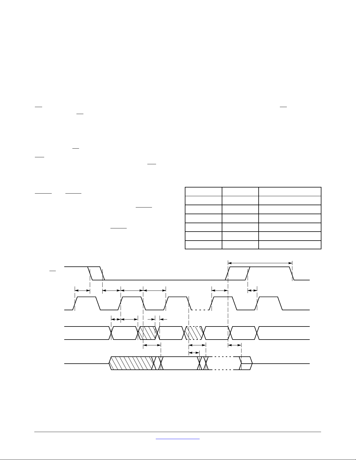
CS
SCK
SI
SO
t
CNH
HI−Z
t
CS
t
CSS
t
SU
VALID
IN
t
WH
t
H
t
WL
t
CSH
t
RI
t
FI
t
V
t
HO
VALID
OUT
t
V
t
DIS
t
CNS
HI−Z
Figure 2. Synchronous Data Timing
www.onsemi.com
4
Page 5

CAT25512
Status Register
The Status Register, as shown in Table 8, contains a
number of status and control bits.
The RDY
(Ready) bit indicates whether the device is busy
with a write operation. This bit is automatically set to 1 during
an internal write cycle, and reset to 0 when the device is ready
to accept commands. For the host, this bit is read only.
The WEL (Write Enable Latch) bit is set/reset by the
WREN/WRDI commands. When set to 1, the device is in a
Write Enable state and when set to 0, the device is in a Write
Disable state.
The BP0 and BP1 (Block Protect) bits determine which
blocks are currently write protected. They are set by the user
with the WRSR command and are non−volatile. The user is
allowed to protect a quarter, one half or the entire memory,
by setting these bits according to Table 9. The protected
blocks then become read−only.
The WPEN (Write Protect Enable) bit acts as an enable for
the WP
pin. Hardware write protection is enabled when the
WP
pin is low and the WPEN bit is 1. This condition
prevents writing to the status register and to the block
Table 8. STATUS REGISTER
7 6 5 4 3 2 1 0
WPEN IPL 0 LIP BP1 BP0 WEL RDY
protected sections of memory. While hardware write
protection is active, only the non−block protected memory
can be written. Hardware write protection is disabled when
pin is high or the WPEN bit is 0. The WPEN bit, WP
the WP
pin and WEL bit combine to either permit or inhibit Write
operations, as detailed in Table 10.
The IPL (Identification Page Latch) bit determines
whether the additional Identification Page (IPL = 1) or main
memory array (IPL = 0) can be accessed both for Read and
Write operations. The IPL bit is set by the user with the
WRSR command and is volatile. The IPL bit is
automatically reset after read/write operations.
The LIP (Lock Identification Page) bit is set by the user
with the WRSR command and is non−volatile. When set to
1, the Identification Page is permanently write protected
(locked in Read−only mode).
Note: The IPL and LIP bits cannot be set to 1 using the same
WRSR instruction. If the user attempts to set (“1”) both the
IPL and LIP bit in the same time, these bits cannot be written
and therefore they will remain unchanged.
Table 9. BLOCK PROTECTION BITS
Status Register Bits
BP1 BP0
0 0 None No Protection
0 1 C000−FFFF Quarter Array Protection
1 0 8000−FFFF Half Array Protection
1 1 0000−FFFF Full Array Protection
Table 10. WRITE PROTECT CONDITIONS
WPEN WP WEL Protected Blocks Unprotected Blocks Status Register
0 X 0 Protected Protected Protected
0 X 1 Protected Writable Writable
1 Low 0 Protected Protected Protected
1 Low 1 Protected Writable Protected
X High 0 Protected Protected Protected
X High 1 Protected Writable Writable
Array Address Protected Protection
www.onsemi.com
5
Page 6

CAT25512
WRITE OPERATIONS
The CAT25512 device powers up into a write disable
state. The device contains a Write Enable Latch (WEL)
which must be set before attempting to write to the memory
array or to the status register. In addition, the address of the
memory location(s) to be written must be outside the
protected area, as defined by BP0 and BP1 bits from the
status register.
CS
SCK
SI
SO
Dashed Line = mode (1, 1)
00000
Figure 3. WREN Timing
Write Enable and Write Disable
The internal Write Enable Latch and the corresponding
Status Register WEL bit are set by sending the WREN
instruction to the CAT25512. Care must be taken to take the
CS
input high after the WREN instruction, as otherwise the
Write Enable Latch will not be properly set. WREN timing
is illustrated in Figure 3. The WREN instruction must be
sent prior to any WRITE or WRSR instruction.
The internal write enable latch is reset by sending the
WRDI instruction as shown in Figure 4. Disabling write
operations by resetting the WEL bit, will protect the device
against inadvertent writes.
110
HIGH IMPEDANCE
CS
SCK
SI
SO
Dashed Line = mode (1, 1)
00000
HIGH IMPEDANCE
Figure 4. WRDI Timing
100
www.onsemi.com
6
Page 7

CAT25512
Byte Write
Once the WEL bit is set, the user may execute a write
Following completion of the write cycle, the CAT25512 is
automatically returned to the write disable state.
sequence, by sending a WRITE instruction, a 16−bit address
and a data byte as shown in Figure 5. Internal programming
will start after the low to high CS
transition. During an
internal write cycle, all commands, except for RDSR (Read
Status Register) will be ignored. The RDY
if the internal write cycle is in progress (RDY
device is ready to accept commands (RDY
bit will indicate
high), or the
low).
Write Identification Page
The additional 128−byte Identification Page (IP) can be
written with user data using the same Write commands
sequence as used for Page Write to the main memory array
(Figure 6). The IPL bit from the Status Register must be set
(IPL = 1) using the WRSR instruction, before attempting
to write to the IP.
Page Write
After sending the first data byte to the CAT25512, the host
may continue sending data, up to a total of 128 bytes,
according to timing shown in Figure 6. After each data byte,
the lower order address bits are automatically incremented,
while the higher order address bits (page address) remain
unchanged. If during this process the end of page is
exceeded, then loading will “roll over” to the first byte in the
page, thus possibly overwriting previously loaded data.
The address bits [A15:A7] are Don’t Care and the
[A6:A0] bits define the byte address within the
Identification Page. In addition, the Byte Address must point
to a location outside the protected area defined by the BP1,
BP0 bits from the Status Register. When the full memory
array is write protected (BP1, BP0 = 1,1), the write
instruction to the IP is not accepted and not executed.
Also, the write to the IP is not accepted if the LIP bit from
the Status Register is set to 1 (the page is locked in
Read−only mode).
Table 11. BYTE ADDRESS
Device Address Significant Bits # Address Clock Pulses
Main Memory Array A15 − A0 16
Identification Page A6 − A0 16
CS
012345678
SCK
SI
SO
CS
SCK
SI
SO
0000 01 0
Dashed Line = mode (1, 1)
012345678 212223
0000 0 10
Dashed Line = mode (1, 1)
OPCODE
0
HIGH IMPEDANCE
OPCODE
0
21 22 23 24 25 26 27 28 29 30 31
BYTE ADDRESS*
D7 D6 D5 D4 D3 D2 D1 D0
A
N
A
0
* Please check the Byte Address Table (Table 11)
Figure 5. Byte WRITE Timing
24−31
BYTE ADDRESS*
A
N
HIGH IMPEDANCE
A
0
Data
Byte 1
* Please check the Byte Address Table (Table 11)
Figure 6. Page WRITE Timing
32−39
DATA IN
Data
Byte 2
DATA IN
24+(N−1)x8−1 .. 24+(N−1)x8
24+Nx8−1
Data Byte N
Data
Byte 3
7..1 0
www.onsemi.com
7
Page 8

CAT25512
Write Status Register
The Status Register is written by sending a WRSR
instruction according to timing shown in Figure 7. Only bits
2, 3, 4, 6 and 7 can be written using the WRSR command.
The internal programming for the SR bits will start after
the low to high CS
last maximum 5 ms (t
transition. The internal write cycle will
).
WC
It is recommended to avoid SR polling routine (through
RDSR) while writing to the status register is in progress
and insert a fixed delay of 5 ms before sending any other
instruction to the CAT25512.
CS
0123 456 78 10911121314
SCK
OPCODE
SI
SO
Dashed Line = mode (1, 1)
0000000 1
HIGH IMPEDANCE
Figure 7. WRSR Timing
Write Protection
The Write Protect (WP) pin can be used to protect the
Block Protect bits BP0 and BP1 against being inadvertently
altered. When WP
is low and the WPEN bit is set to “1”,
write operations to the Status Register are inhibited. WP
going low while CS is still low will interrupt a write to the
status register. If the internal write cycle has already been
initiated, WP
operation to the Status Register. The WP
going low will have no effect on any write
pin function is
blocked when the WPEN bit is set to “0”. The WP
timing is shown in Figure 8.
15
DATA IN
7 6 5 4 3 2 10
MSB
input
CS
SCK
WP
WP
Dashed Line = mode (1, 1)
t
WPS
Figure 8. WP Timing
t
WPH
www.onsemi.com
8
Page 9

CAT25512
READ OPERATIONS
Read from Memory Array
To read from memory, the host sends a READ instruction
followed by a 16−bit address.
After receiving the last address bit, the CAT25512 will
respond by shifting out data on the SO pin (as shown in
Figure 9). Sequentially stored data can be read out by simply
continuing to run the clock. The internal address pointer is
automatically incremented to the next higher address as data
is shifted out. After reaching the highest memory address,
the address counter “rolls over” to the lowest memory
address, and the read cycle can be continued indefinitely.
The read operation is terminated by taking CS
Read Identification Page
high.
Reading the additional 128−byte Identification Page (IP)
is achieved using the same Read command sequence as used
for Read from main memory array (Figure 9). The IPL bit
from the Status Register must be set (IPL = 1) before
attempting to read from the IP. The [A6:A0] are the address
significant bits that point to the data byte shifted out on the
CS
SO pin. If the CS continues to be held low, the internal
address register defined by [A6:A0] bits is automatically
incremented and the next data byte from the IP is shifted out.
The byte address must not exceed the 128−byte page
boundary.
Read Status Register
To read the status register, the host simply sends a RDSR
command. After receiving the last bit of the command, the
CAT25512 will shift out the contents of the status register on
the SO pin (Figure 10). The status register may be read at
any time, including during an internal write cycle.
While the internal write cycle is in progress, the RDSR
command will output the full content of the status register.
For easy detection of the internal write cycle completion,
both during writing to the memory array and to the status
register, we recommend sampling the RDY bit only through
the polling routine. After detecting the RDY bit “0”, the next
RDSR instruction will always output the expected content
of the status register.
0123456789
SCK
OPCODE
SI
SO
CS
SCK
SI
SO
00 00 0 11
Dashed Line = mode (1, 1)
* Please check the Byte Address Table (Table 11)
0123 4 56 78 10911121314
00000 1 01
Dashed Line = mode (1, 1)
0
HIGH IMPEDANCE
OPCODE
HIGH IMPEDANCE
10
BYTE ADDRESS*
A
N
Figure 9. READ Timing
Figure 10. RDSR Timing
2120 22 23 24 25 26 27 28 29 30
7 6
MSB
A
0
DATA OUT
7
6 5 4 3 2 1 0
MSB
DATA OUT
5
4 3 2 1 0
www.onsemi.com
9
Page 10

CAT25512
Hold Operation
The HOLD input can be used to pause communication
between host and CAT25512. To pause, HOLD
must be
taken low while SCK is low (Figure 11). During the hold
condition the device must remain selected (CS
low). During
the pause, the data output pin (SO) is tri−stated (high
impedance) and SI transitions are ignored. To resume
communication, HOLD
must be taken high while SCK is low.
Design Considerations
The CAT25512 device incorporates Power−On Reset
(POR) circuitry which protects the internal logic against
powering up in the wrong state. The device will power up
into Standby mode after V
and will power down into Reset mode when V
CS
SCK
HOLD
exceeds the POR trigger level
CC
CC
t
CD
t
HD
drops
below the POR trigger level. This bi−directional POR
behavior protects the device against ‘brown−out’ failure
following a temporary loss of power.
The CAT25512 device powers up in a write disable state
and in a low power standby mode. A WREN instruction
must be issued prior to any writes to the device.
After power up, the CS pin must be brought low to enter
a ready state and receive an instruction. After a successful
byte/page write or status register write, the device goes into
a write disable mode. The CS input must be set high after the
proper number of clock cycles to start the internal write
cycle. Access to the memory array during an internal write
cycle is ignored and programming is continued. Any invalid
op−code will be ignored and the serial output pin (SO) will
remain in the high impedance state.
t
CD
t
HD
SO
Dashed Line = mode (1, 1)
t
HZ
Figure 11. HOLD Timing
HIGH IMPEDANCE
t
LZ
www.onsemi.com
10
Page 11

CAT25512
ORDERING INFORMATION
Device Order
Number
CAT25512HU5E−GT3 S9L UDFN8 −40°C to +125°C 2.5 V NiPdAu Tape & Reel,
CAT25512HU5I−GT3 S9L UDFN8 −40°C to +85°C 1.8 V NiPdAu Tape & Reel,
CAT25512VE−GT3 25512A SOIC−8,
CAT25512VI−GT3 25512A SOIC−8,
CAT25512XE−T2 25512A SOIC−8,
CAT25512XI−T2 25512A SOIC−8,
CAT25512YE−GT3 S12A TSSOP−8 −40°C to +125°C 2.5 V NiPdAu Tape & Reel,
CAT25512YI−GT3 S12A TSSOP−8 −40°C to +85°C 1.8 V NiPdAu Tape & Reel,
†For information on tape and reel specifications, including part orientation and tape sizes, please refer to our Tape and Reel Packaging
Specifications Brochure, BRD8011/D.
9. For additional package and temperature options, please contact your nearest ON Semiconductor Sales office.
10.For detailed information and a breakdown of device nomenclature and numbering systems, please see the ON Semiconductor Device
Nomenclature document, TND310/D, available at www.onsemi.com
Specific
Device
Marking
Package
Type
JEDEC
JEDEC
JEDEC
JEDEC
V
CC
Temperature Range
−40°C to +125°C 2.5 V NiPdAu Tape & Reel,
−40°C to +85°C 1.8 V NiPdAu Tape & Reel,
−40°C to +125°C 2.5 V Matte−Tin Tape & Reel,
−40°C to +85°C 1.8 V Matte−Tin Tape & Reel,
Range
Lead
Finish
Shipping
3,000 Units / Reel
3,000 Units / Reel
3,000 Units / Reel
3,000 Units / Reel
2,000 Units / Reel
2,000 Units / Reel
3,000 Units / Reel
3,000 Units / Reel
†
www.onsemi.com
11
Page 12

MECHANICAL CASE OUTLINE
PACKAGE DIMENSIONS
SCALE 4:1
B
A1
A
E
A
SEATING
C
PLANE
PIN 1
REFERENCE
NOTE 4
C0.15
C0.05
C0.05
C0.15
TOP VIEW
SIDE VIEW
D
DETAIL A
UDFN8 3.0x2.0, 0.5P
CASE 517BU−01
ISSUE O
(0.127)
DETAIL A
(0.065)
DATE 06 APR 2011
NOTES:
1. DIMENSIONING AND TOLERANCING PER
ASME Y14.5M, 1994.
2. CONTROLLING DIMENSION: MILLIMETERS.
3. DIMENSIONS b APPLIES TO PLATED
TERMINAL AND IS MEASURED BETWEEN
0.15 AND 0.25 MM FROM TERMINAL TIP.
4. COPLANARITY APPLIES TO THE EXPOSED
PAD AS WELL AS THE TERMINALS.
MILLIMETERS
DIM MIN MAX
A
0.45 0.55
A1 0.00 0.05
b 0.20 0.30
D 2.00 BSC
D2 1.35 1.45
E 3.00 BSC
E2 0.85 0.95
e 0.50 BSC
L 0.35 0.45
GENERIC
MARKING DIAGRAM*
D2
1
8
e
BOTTOM VIEW
RECOMMENDED
MOUNTING FOOTPRINT
1.56
8X
0.63
PKG
OUTLINE
1
0.50
PITCH
DIMENSIONS: MILLIMETERS
4
5
M
0.10 BC
8X
L
0.10 BC
E2
8X
b
0.10
0.05
1.06
8X
0.32
3.30
A
XXX
ALL
YM
G
M
A
XXX = Specific Device Code
A = Assembly Location Code
LL = Assembly Lot
Y = Year
M = Month
G = Pb−Free Package
M
M
B
AC
NOTE 3
C
D
*This information is generic. Please refer to
device data sheet for actual part marking.
Pb−Free indicator, “G” or microdot “ G”,
may or may not be present.
DOCUMENT NUMBER:
DESCRIPTION:
ON Semiconductor and are trademarks of Semiconductor Components Industries, LLC dba ON Semiconductor or its subsidiaries in the United States and/or other countries.
ON Semiconductor reserves the right to make changes without further notice to any products herein. ON Semiconductor makes no warranty, representation or guarantee regarding
the suitability of its products for any particular purpose, nor does ON Semiconductor assume any liability arising out of the application or use of any product or circuit, and specifically
disclaims any and all liability, including without limitation special, consequential or incidental damages. ON Semiconductor does not convey any license under its patent rights nor the
rights of others.
© Semiconductor Components Industries, LLC, 2019
98AON55336E
UDFN8 3.0 X 2.0, 0.5P
Electronic versions are uncontrolled except when accessed directly from the Document Repository.
Printed versions are uncontrolled except when stamped “CONTROLLED COPY” in red.
PAGE 1 OF 1
www.onsemi.com
Page 13

MECHANICAL CASE OUTLINE
PACKAGE DIMENSIONS
E1 E
PIN # 1
IDENTIFICATION
SOIC 8, 150 mils
CASE 751BD−01
ISSUE O
DATE 19 DEC 2008
SYMBOL MIN NOM MAX
A
A1
b
c
D
E
E1
e
h
L
θ
1.35
0.10
0.33
0.19
4.80
5.80
3.80
1.27 BSC
0.25
0.40 1.27
1.75
0.25
0.51
0.25
5.00
6.20
4.00
0.50
0º 8º
TOP VIEW
D
A1
A
e
SIDE VIEW
Notes:
(1) All dimensions are in millimeters. Angles in degrees.
(2) Complies with JEDEC MS-012.
b
h
θ
c
L
END VIEW
DOCUMENT NUMBER:
DESCRIPTION:
ON Semiconductor and are trademarks of Semiconductor Components Industries, LLC dba ON Semiconductor or its subsidiaries in the United States and/or other countries.
ON Semiconductor reserves the right to make changes without further notice to any products herein. ON Semiconductor makes no warranty, representation or guarantee regarding
the suitability of its products for any particular purpose, nor does ON Semiconductor assume any liability arising out of the application or use of any product or circuit, and specifically
disclaims any and all liability, including without limitation special, consequential or incidental damages. ON Semiconductor does not convey any license under its patent rights nor the
rights of others.
© Semiconductor Components Industries, LLC, 2019
98AON34272E
SOIC 8, 150 MILS
Electronic versions are uncontrolled except when accessed directly from the Document Repository.
Printed versions are uncontrolled except when stamped “CONTROLLED COPY” in red.
PAGE 1 OF 1
www.onsemi.com
Page 14

MECHANICAL CASE OUTLINE
PACKAGE DIMENSIONS
E1
SOIC−8, 208 mils
CASE 751BE−01
ISSUE O
E
DATE 19 DEC 2008
SYMBOL MIN NOM MAX
A1
E1
A
0.05
b
c
D
E
e
L
θ
0.36
0.19
5.13
7.75
5.13
1.27 BSC
0.51 0.76
0º 8º
2.03
0.25
0.48
0.25
5.33
8.26
5.38
PIN#1 IDENTIFICATION
TOP VIEW
D
A
eb
SIDE VIEW
Notes:
(1) All dimensions are in millimeters. Angles in degrees.
(2) Complies with EIAJ EDR-7320.
A1
q
L
END VIEW
c
DOCUMENT NUMBER:
DESCRIPTION:
ON Semiconductor and are trademarks of Semiconductor Components Industries, LLC dba ON Semiconductor or its subsidiaries in the United States and/or other countries.
ON Semiconductor reserves the right to make changes without further notice to any products herein. ON Semiconductor makes no warranty, representation or guarantee regarding
the suitability of its products for any particular purpose, nor does ON Semiconductor assume any liability arising out of the application or use of any product or circuit, and specifically
disclaims any and all liability, including without limitation special, consequential or incidental damages. ON Semiconductor does not convey any license under its patent rights nor the
rights of others.
© Semiconductor Components Industries, LLC, 2019
98AON34273E
SOIC−8, 208 MILS
Electronic versions are uncontrolled except when accessed directly from the Document Repository.
Printed versions are uncontrolled except when stamped “CONTROLLED COPY” in red.
PAGE 1 OF 1
www.onsemi.com
Page 15

MECHANICAL CASE OUTLINE
PACKAGE DIMENSIONS
b
E
E1
TSSOP8, 4.4x3
CASE 948AL−01
ISSUE O
SYMBOLθMIN NOM MAX
A1
A2
E1
L1
DATE 19 DEC 2008
A
0.05
0.80
b
c
D
E
e
L
0.19
0.09
2.90
6.30
4.30
0.50
0.90
3.00
6.40
4.40
0.65 BSC
1.00 REF
0.60
1.20
0.15
1.05
0.30
0.20
3.10
6.50
4.50
0.75
0º 8º
e
TOP VIEW
D
A2
SIDE VIEW
Notes:
(1) All dimensions are in millimeters. Angles in degrees.
(2) Complies with JEDEC MO-153.
A
A1
q1
L1
c
L
END VIEW
DOCUMENT NUMBER:
DESCRIPTION:
ON Semiconductor and are trademarks of Semiconductor Components Industries, LLC dba ON Semiconductor or its subsidiaries in the United States and/or other countries.
ON Semiconductor reserves the right to make changes without further notice to any products herein. ON Semiconductor makes no warranty, representation or guarantee regarding
the suitability of its products for any particular purpose, nor does ON Semiconductor assume any liability arising out of the application or use of any product or circuit, and specifically
disclaims any and all liability, including without limitation special, consequential or incidental damages. ON Semiconductor does not convey any license under its patent rights nor the
rights of others.
© Semiconductor Components Industries, LLC, 2019
98AON34428E
TSSOP8, 4.4X3
Electronic versions are uncontrolled except when accessed directly from the Document Repository.
Printed versions are uncontrolled except when stamped “CONTROLLED COPY” in red.
PAGE 1 OF 1
www.onsemi.com
Page 16

ON Semiconductor and are trademarks of Semiconductor Components Industries, LLC dba ON Semiconductor or its subsidiaries in the United States and/or other countries.
ON Semiconductor owns the rights to a number of patents, trademarks, copyrights, trade secrets, and other intellectual property. A listing of ON Semiconductor’s product/patent
coverage may be accessed at www.onsemi.com/site/pdf/Patent−Marking.pdf
ON Semiconductor makes no warranty, representation or guarantee regarding the suitability of its products for any particular purpose, nor does ON Semiconductor assume any liability
arising out of the application or use of any product or circuit, and specifically disclaims any and all liability, including without limitation special, consequential or incidental damages.
Buyer is responsible for its products and applications using ON Semiconductor products, including compliance with all laws, regulations and safety requirements or standards,
regardless of any support or applications information provided by ON Semiconductor. “Typical” parameters which may be provided in ON Semiconductor data sheets and/or
specifications can and do vary in different applications and actual performance may vary over time. All operating parameters, including “Typicals” must be validated for each customer
application by customer’s technical experts. ON Semiconductor does not convey any license under its patent rights nor the rights of others. ON Semiconductor products are not
designed, intended, or authorized for use as a critical component in life support systems or any FDA Class 3 medical devices or medical devices with a same or similar classification
in a foreign jurisdiction or any devices intended for implantation in the human body. Should Buyer purchase or use ON Semiconductor products for any such unintended or unauthorized
application, Buyer shall indemnify and hold ON Semiconductor and its officers, employees, subsidiaries, affiliates, and distributors harmless against all claims, costs, damages, and
expenses, and reasonable attorney fees arising out of, directly or indirectly, any claim of personal injury or death associated with such unintended or unauthorized use, even if such
claim alleges that ON Semiconductor was negligent regarding the design or manufacture of the part. ON Semiconductor is an Equal Opportunity/Affirmative Action Employer. This
literature is subject to all applicable copyright laws and is not for resale in any manner.
. ON Semiconductor reserves the right to make changes without further notice to any products herein.
PUBLICATION ORDERING INFORMATION
LITERATURE FULFILLMENT:
Email Requests to: orderlit@onsemi.com
ON Semiconductor Website: www.onsemi.com
TECHNICAL SUPPORT
North American Technical Support:
Voice Mail: 1 800−282−9855 Toll Free USA/Canada
Phone: 011 421 33 790 2910
Europe, Middle East and Africa Technical Support:
Phone: 00421 33 790 2910
For additional information, please contact your local Sales Representative
◊
www.onsemi.com
1
 Loading...