

Page 1
CAT24C01, CAT24C02,
CAT24C04, CAT24C08,
CAT24C16
1-Kb, 2-Kb, 4-Kb, 8-Kb and
2
16-Kb I
C CMOS Serial
EEPROM
http://onsemi.com
Description
The CAT24C01/02/04/08/16 are 1−Kb, 2−Kb, 4−Kb, 8−Kb and
16−Kb respectively CMOS Serial EEPROM devices organized
internally as 8/16/32/64 and 128 pages respectively of 16 bytes each.
All devices support both the Standard (100 kHz) as well as Fast
(400 kHz) I
2
C protocol.
Data is written by providing a starting address, then loading 1 to 16
contiguous bytes into a Page Write Buffer, and then writing all data to
non−volatile memory in one internal write cycle. Data is read by
providing a starting address and then shifting out data serially while
automatically incrementing the internal address count.
External address pins make it possible to address up to eight
CAT24C01 or CAT24C02, four CAT24C04, two CAT24C08 and one
CAT24C16 device on the same bus.
Features
• Supports Standard and Fast I
2
C Protocol
• 1.7 V to 5.5 V Supply Voltage Range
• 16−Byte Page Write Buffer
• Hardware Write Protection for Entire Memory
• Schmitt Triggers and Noise Suppression Filters on I
(SCL and SDA)
2
C Bus Inputs
• Low power CMOS Technology
• More than 1,000,000 Program/Erase Cycles
• 100 Year Data Retention
• Industrial and Extended Temperature Range
• These Devices are Pb−Free, Halogen Free/BFR Free and are RoHS
Compliant
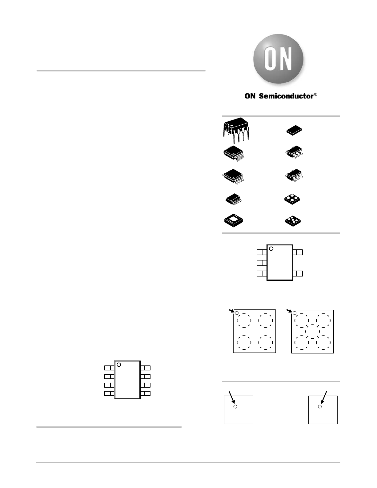
PIN CONFIGURATION
CAT24C__
16 / 08 / 04 / 02 / 01
////
NC
NC NC
////
NC NC
NC
A1A1A
////
A2A2A
A
2
A
A
0
0
1
2
V
SS
8
1
7
2
6
3
5
4
V
CC
WP
SCL
SDA
PDIP−8
L SUFFIX
CASE 646AA
MSOP−8
Z SUFFIX
CASE 846AD
TSSOP−8
Y SUFFIX
CASE 948AL
SOIC−8
W SUFFIX
CASE 751BD
TDFN−8*
VP2 SUFFIX
CASE 511AK
UDFN8−EP
HU4 SUFFIX
CASE 517AZ
TSOT−23
TD SUFFIX
CASE 419AE
TSOP−5**
TS SUFFIX
CASE 483
WLCSP−4***
C4A SUFFIX
CASE 567DC
WLCSP−5***
C5A SUFFIX
CASE 567DD
PIN CONFIGURATIONS
SCL
V
SS
SDA
TSOT−23 (TD), TSOP−5** (TS) (Top View)
** TSOP are available for the CAT24C02 only.
Pin 1
A
V
B
SCL SDA
WLCSP−4*** WLCSP−5***
*** WLCSP are available for the CAT24C04,
CAT24C08 and CAT24C16 only.
Pin 1
V
CC
SS
(Top Views)
TOP MARKING FOR WLCSP
(Ball Down)
5
1
2
3
4
Pin 1
WP
V
CC
12312
V
CC
SDA
WP SCL
A
V
SS
B
C
Pin 1
PDIP (L), SOIC (W), TSSOP (Y), MSOP (Z),
TDFN, (VP2)*, UDFN−EP (HU4) (Top View)
* The TDFN (VP2) package is not recommended for new designs.
ORDERING INFORMATION
See detailed ordering and shipping information in the package
dimensions section on page 19 of this data sheet.
© Semiconductor Components Industries, LLC, 2013
February, 2013 − Rev. 26
X X
Y M Y M
WLCSP−4 WLCSP−5
Y = Production Year (Last Digit)
M = Production Month (1−9, O, N, D)
1 Publication Order Number:
X = Specific Device
X = Code
4 = 24C04
8 = 24C08
6 = 24C16
CAT24C01/D
Page 2
CAT24C01, CAT24C02, CAT24C04, CAT24C08, CAT24C16
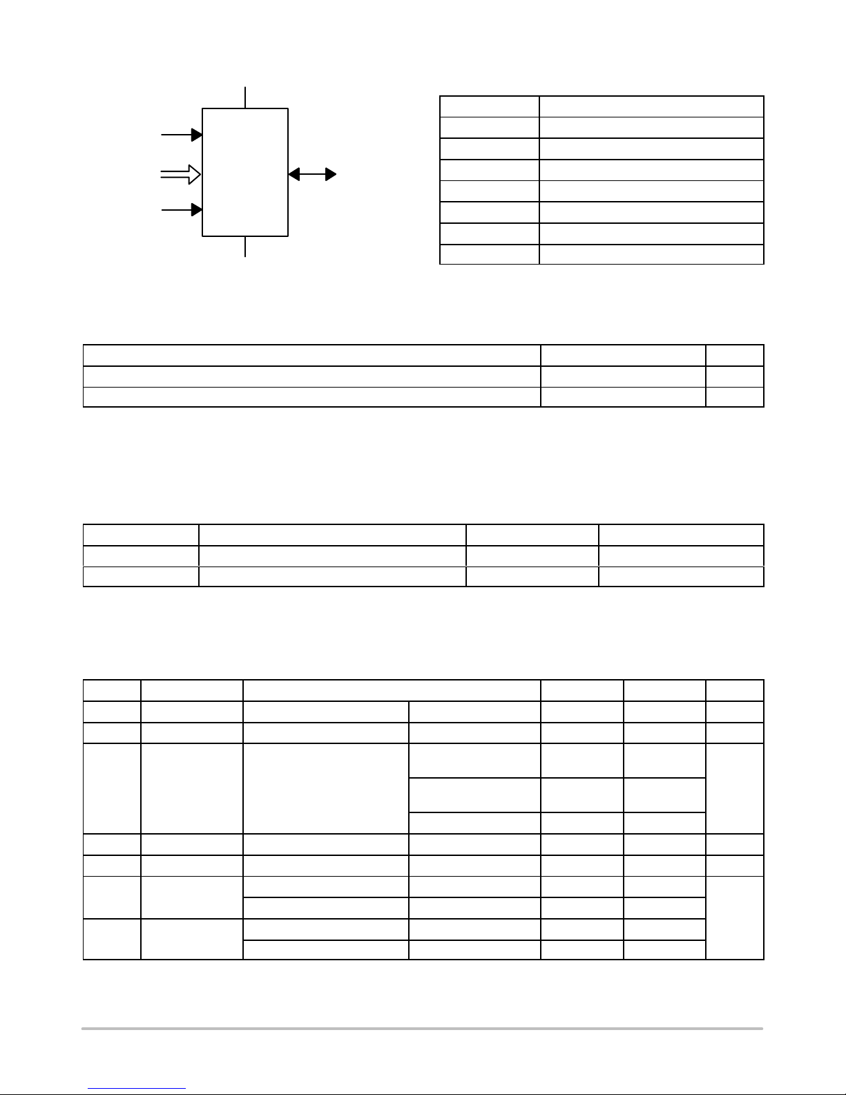
V
CC
SCL
A2, A1, A
0
CAT24Cxx
SDA
WP
V
SS
Figure 1. Functional Symbol
Table 2. ABSOLUTE MAXIMUM RATINGS
Parameters Ratings Units
Storage Temperature −65 to +150 °C
Voltage on any pin with respect to Ground (Note 1) −0.5 to +6.5 V
Stresses exceeding Maximum Ratings may damage the device. Maximum Ratings are stress ratings only. Functional operation above the
Recommended Operating Conditions is not implied. Extended exposure to stresses above the Recommended Operating Conditions may affect
device reliability.
1. During input transitions, voltage undershoot on any pin should not exceed −1 V for more than 20 ns. Voltage overshoot on pins A
and WP should not exceed VCC + 1 V for more than 20 ns, while voltage on the I2C bus pins, SCL and SDA, should not exceed the absolute
maximum ratings, irrespective of V
CC
.
Table 1. PIN FUNCTION
Pin Name
A0, A1, A2 Device Address Input
†The exposed pad for the TDFN/UDFN packages can be left floating
or connected to Ground.
†
Function
SDA Serial Data Input/Output
SCL Serial Clock Input
WP Write Protect Input
V
CC
V
SS
Power Supply
Ground
NC No Connect
, A1, A
0
2
Table 3. RELIABILITY CHARACTERISTICS (Note 2)
Symbol
N
(Note 3) Endurance 1,000,000 Program / Erase Cycles
END
T
DR
Data Retention 100 Years
2. These parameters are tested initially and after a design or process change that affects the parameter according to appropriate AEC−Q100
and JEDEC test methods.
3. Page Mode, V
= 5 V, 25°C.
CC
Parameter Min Units
Table 4. D.C. OPERATING CHARACTERISTICS
(VCC = 1.8 V to 5.5 V, TA = −40°C to +125°C and VCC = 1.7 V to 5.5 V, TA = −40°C to +85°C, unless otherwise specified.)
Symbol
I
CCR
I
CCW
I
SB
I
L
V
IL
V
IH
V
OL
Parameter Test Conditions Min Max Units
Read Current Read, f
Write Current Write, f
Standby Current All I/O Pins at GND or V
= 400 kHz 1 mA
SCL
= 400 kHz 2 mA
SCL
TA = −40°C to +85°C
CC
V
CC
TA = −40°C to +85°C
V
CC
≤ 3.3 V
> 3.3 V
1 mA
3
TA = −40°C to +125°C 5
I/O Pin Leakage Pin at GND or V
CC
Input Low Voltage −0.5 0.3 x V
Input High Voltage
Output Low
Voltage
A0, A1, A2 and WP 0.7 x V
SCL and SDA 0.7 x V
CC
CC
VCC > 2.5 V, IOL = 3 mA 0.4
VCC < 2.5 V, IOL = 1 mA 0.2
2
CC
VCC + 0.5
5.5
mA
V
V
http://onsemi.com
2
Page 3

CAT24C01, CAT24C02, CAT24C04, CAT24C08, CAT24C16
Table 5. PIN IMPEDANCE CHARACTERISTICS
(VCC = 1.8 V to 5.5 V, TA = −40°C to +125°C and VCC = 1.7 V to 5.5 V, TA = −40°C to +85°C, unless otherwise specified.)
Symbol
C
(Note 4)
IN
SDA Pin Capacitance
Other Pins 6 pF
IWP (Note 5) WP Input Current
IA (Note 5) Address Input Current
(A0, A1, A2)
Product Rev H: CAT24C02
Product Rev K: CAT24C04,
CAT24C08, CAT24C16
4. These parameters are tested initially and after a design or process change that affects the parameter according to appropriate AEC−Q100
and JEDEC test methods.
5. When not driven, the WP, A0, A1 and A2 pins are pulled down to GND internally. For improved noise immunity, the internal pull−down is
relatively strong; therefore the external driver must be able to supply the pull−down current when attempting to drive the input HIGH. To
conserve power, as the input level exceeds the trip point of the CMOS input buffer (~ 0.5 x VCC), the strong pull−down reverts to a weak
current source.
Table 6. A.C. CHARACTERISTICS
(Note 6) (VCC = 1.8 V to 5.5 V, TA = −40°C to +125°C and VCC = 1.7 V to 5.5 V, TA = −40°C to +85°C, unless otherwise specified.)
Symbol
F
SCL
t
HD:STA
t
LOW
t
HIGH
t
SU:STA
t
HD:DAT
t
SU:DAT
t
R
tF (Note 6) SDA and SCL Fall Time 300 300 ns
t
SU:STO
t
BUF
t
AA
t
DH
Ti (Note 6) Noise Pulse Filtered at SCL and SDA Inputs 100 100 ns
t
SU:WP
t
HD:WP
t
WR
tPU (Notes 7, 8) Power−up to Ready Mode 1 1 ms
6. Test conditions according to “AC Test Conditions” table.
7. Tested initially and after a design or process change that affects this parameter.
is the delay between the time VCC is stable and the device is ready to accept commands.
8. t
PU
Clock Frequency 100 400 kHz
START Condition Hold Time 4 0.6
Low Period of SCL Clock 4.7 1.3
High Period of SCL Clock 4 0.6
START Condition Setup Time 4.7 0.6
Data In Hold Time 0 0
Data In Setup Time 250 100 ns
SDA and SCL Rise Time 1000 300 ns
STOP Condition Setup Time 4 0.6
Bus Free Time Between STOP and START 4.7 1.3
SCL Low to Data Out Valid 3.5 0.9
Data Out Hold Time 100 100 ns
WP Setup Time 0 0
WP Hold Time 2.5 2.5
Write Cycle Time 5 5 ms
Parameter Conditions Max Units
VIN = 0 V, f = 1.0 MHz, VCC = 5.0 V
8 pF
VIN < VIH, VCC = 5.5 V 130 mA
VIN < VIH, VCC = 3.3 V 120
VIN < VIH, VCC = 1.7 V 80
VIN > V
IH
2
VIN < VIH, VCC = 5.5 V 50 mA
VIN < VIH, VCC = 3.3 V 35
VIN < VIH, VCC = 1.7 V 25
VIN > V
IH
2
Standard Fast
Parameter
Min Max Min Max
Units
ms
ms
ms
ms
ms
ms
ms
ms
ms
ms
http://onsemi.com
3
Page 4

CAT24C01, CAT24C02, CAT24C04, CAT24C08, CAT24C16
Table 7. A.C. TEST CONDITIONS
Input Drive Levels 0.2 x VCC to 0.8 x V
Input Rise and Fall Time v 50 ns
Input Reference Levels 0.3 x VCC, 0.7 x V
Output Reference Level 0.5 x V
Output Test Load Current Source IOL = 3 mA (VCC w 2.5 V); IOL = 1 mA (V
CC
CC
CC
< 2.5 V); CL = 100 pF
CC
Power−On Reset (POR)
Each CAT24Cxx* incorporates Power−On Reset (POR)
circuitry which protects the internal logic against powering
up in the wrong state.
A CAT24Cxx device will power up into Standby mode
after V
down into Reset mode when V
exceeds the POR trigger level and will power
CC
drops below the POR
CC
trigger level. This bi−directional POR feature protects the
device against ‘brown−out’ failure following a temporary
loss of power.
*For common features, the CAT24C01/02/04/08/16 will be
referred to as CAT24Cxx.
Pin Description
SCL: The Serial Clock input pin accepts the Serial Clock
generated by the Master.
SDA: The Serial Data I/O pin receives input data and
transmits data stored in EEPROM. In transmit mode, this pin
is open drain. Data is acquired on the positive edge, and is
delivered on the negative edge of SCL.
A0, A1 and A2: The Address inputs set the device address
when cascading multiple devices. When not driven, these
pins are pulled LOW internally.
WP: The Write Protect input pin inhibits all write
operations, when pulled HIGH. When not driven, this pin is
pulled LOW internally.
Functional Description
The CAT24Cxx supports the Inter−Integrated Circuit
2
(I
C) Bus data transmission protocol, which defines a device
that sends data to the bus as a transmitter and a device
receiving data as a receiver. Data flow is controlled by a
Master device, which generates the serial clock and all
START and STOP conditions. The CAT24Cxx acts as a
Slave device. Master and Slave alternate as either
transmitter or receiver.
I2C Bus Protocol
The I2C bus consists of two ‘wires’, SCL and SDA. The
two wires are connected to the V
supply via pull−up
CC
resistors. Master and Slave devices connect to the 2−wire
bus via their respective SCL and SDA pins. The transmitting
device pulls down the SDA line to ‘transmit’ a ‘0’ and
releases it to ‘transmit’ a ‘1’.
Data transfer may be initiated only when the bus is not
busy (see AC Characteristics).
During data transfer, the SDA line must remain stable
while the SCL line is high. An SDA transition while SCL is
high will be interpreted as a START or STOP condition
(Figure 2). The START condition precedes all commands. It
consists of a HIGH to LOW transition on SDA while SCL
is HIGH. The START acts as a ‘wake−up’ call to all
receivers. Absent a START, a Slave will not respond to
commands. The STOP condition completes all commands.
It consists of a LOW to HIGH transition on SDA while SCL
is HIGH.
NOTE: The I/O pins of CAT24Cxx do not obstruct the SCL
and SDA lines if the VCC supply is switched off. During
power−up, the SCL and SDA pins (connected with pull−up
resistors to VCC) will follow the VCC monotonically from
VSS (0 V) to nominal VCC value, regardless of pull−up
resistor value. The delta between the VCC and the
instantaneous voltage levels during power ramping will be
determined by the relation between bus time constant
(determined by pull−up resistance and bus capacitance) and
actual VCC ramp rate.
Device Addressing
The Master initiates data transfer by creating a START
condition on the bus. The Master then broadcasts an 8−bit
serial Slave address. For normal Read/Write operations, the
first 4 bits of the Slave address are fixed at 1010 (Ah). The
next 3 bits are used as programmable address bits when
cascading multiple devices and/or as internal address bits.
The last bit of the slave address, R/W, specifies whether a
Read (1) or Write (0) operation is to be performed. The 3
address space extension bits are assigned as illustrated in
Figure 3. A
address pins, and a
Acknowledge
, A1 and A0 must match the state of the external
2
, a9 and a8 are internal address bits.
10
After processing the Slave address, the Slave responds
with an acknowledge (ACK) by pulling down the SDA line
during the 9th clock cycle (Figure 4). The Slave will also
acknowledge the address byte and every data byte presented
in Write mode. In Read mode the Slave shifts out a data byte,
and then releases the SDA line during the 9
th
clock cycle. As
long as the Master acknowledges the data, the Slave will
continue transmitting. The Master terminates the session by
not acknowledging the last data byte (NoACK) and by
issuing a STOP condition. Bus timing is illustrated in
Figure 5.
http://onsemi.com
4
Page 5
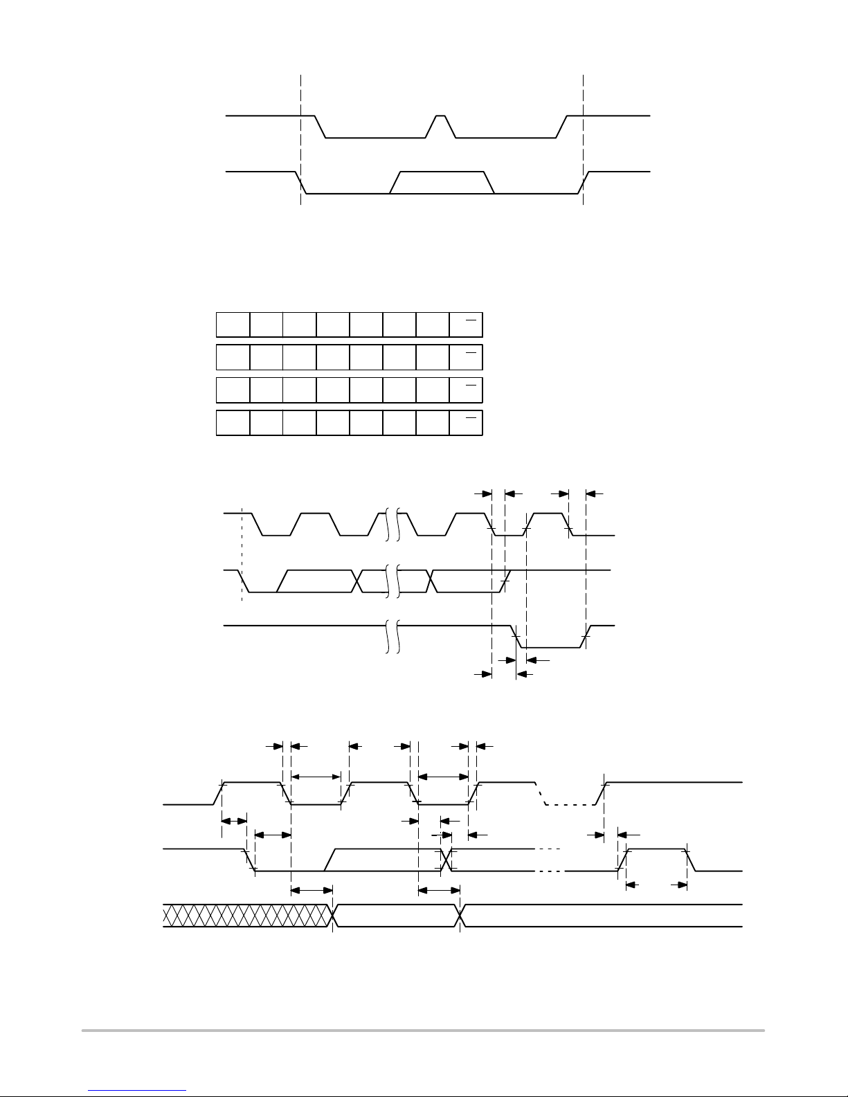
CAT24C01, CAT24C02, CAT24C04, CAT24C08, CAT24C16
SCL
SDA
SCL FROM
MASTER
DATA OUTPUT
FROM TRANSMITTER
START
CONDITION
STOP
CONDITION
Figure 2. Start/Stop Timing
1010A2A1A0R/W CAT24C01 and CAT24C02
1010A2A1a8R/W CAT24C04
1010A2a9a8R/W CAT24C08
1010a
10a9
a8R/W CAT24C16
Figure 3. Slave Address Bits
BUS RELEASE DELAY (TRANSMITTER) BUS RELEASE DELAY
189
(RECEIVER)
DATA OUTPUT
FROM RECEIVER
SCL
SDA IN
SDA OUT
t
SU:STA
START
ACK DELAY (v t
AA
ACK SETUP (w t
)
SU:DAT
)
Figure 4. Acknowledge Timing
t
F
t
LOW
t
HD:SDA
t
HIGH
t
LOW
t
HD:DAT
t
AA
t
R
t
SU:DAT
t
DH
t
SU:STO
t
BUF
Figure 5. Bus Timing
http://onsemi.com
5
Page 6

CAT24C01, CAT24C02, CAT24C04, CAT24C08, CAT24C16
WRITE OPERATIONS
Byte Write
In Byte Write mode, the Master sends the START
condition and the Slave address with the R/W bit set to zero
to the Slave. After the Slave generates an acknowledge, the
Master sends the byte address that is to be written into the
address pointer of the CAT24Cxx. After receiving another
acknowledge from the Slave, the Master transmits the data
byte to be written into the addressed memory location. The
CAT24Cxx device will acknowledge the data byte and the
Master generates the STOP condition, at which time the
device begins its internal Write cycle to nonvolatile memory
(Figure 6). While this internal cycle is in progress (t
WR
), the
SDA output will be tri−stated and the CAT24Cxx will not
respond to any request from the Master device (Figure 7).
Page Write
The CAT24Cxx writes up to 16 bytes of data in a single
write cycle, using the Page Write operation (Figure 8). The
Page Write operation is initiated in the same manner as the
Byte Write operation, however instead of terminating after
the data byte is transmitted, the Master is allowed to send up
to fifteen additional bytes. After each byte has been
transmitted the CAT24Cxx will respond with an
acknowledge and internally increments the four low order
address bits. The high order bits that define the page address
remain unchanged. If the Master transmits more than sixteen
bytes prior to sending the STOP condition, the address
counter ‘wraps around’ to the beginning of page and
previously transmitted data will be overwritten. Once all
sixteen bytes are received and the STOP condition has been
sent by the Master, the internal Write cycle begins. At this
point all received data is written to the CAT24Cxx in a single
write cycle.
Acknowledge Polling
The acknowledge (ACK) polling routine can be used to
take advantage of the typical write cycle time. Once the stop
condition is issued to indicate the end of the host’s write
operation, the CAT24Cxx initiates the internal write cycle.
The ACK polling can be initiated immediately. This
involves issuing the start condition followed by the slave
address for a write operation. If the CAT24Cxx is still busy
with the write operation, NoACK will be returned. If the
CAT24Cxx has completed the internal write operation, an
ACK will be returned and the host can then proceed with the
next read or write operation.
Hardware Write Protection
With the WP pin held HIGH, the entire memory is
protected against Write operations. If the WP pin is left
floating or is grounded, it has no impact on the operation of
the CAT24Cxx. The state of the WP pin is strobed on the last
falling edge of SCL immediately preceding the first data
byte (Figure 9). If the WP pin is HIGH during the strobe
interval, the CAT24Cxx will not acknowledge the data byte
and the Write request will be rejected.
Delivery State
The CAT24Cxx is shipped erased, i.e., all bytes are FFh.
BUS ACTIVITY:
MASTER
SLAVE
* For the CAT24C01 a
S
T
A
SLAVE
R
ADDRESS
T
S
= 0
7
Figure 6. Byte Write Sequence
A
C
K
ADDRESS
BYTE
a
DATA
BYTE
− a
7
0
d7− d
0
A
C
K
S
T
O
P
P
A
C
K
http://onsemi.com
6
Page 7
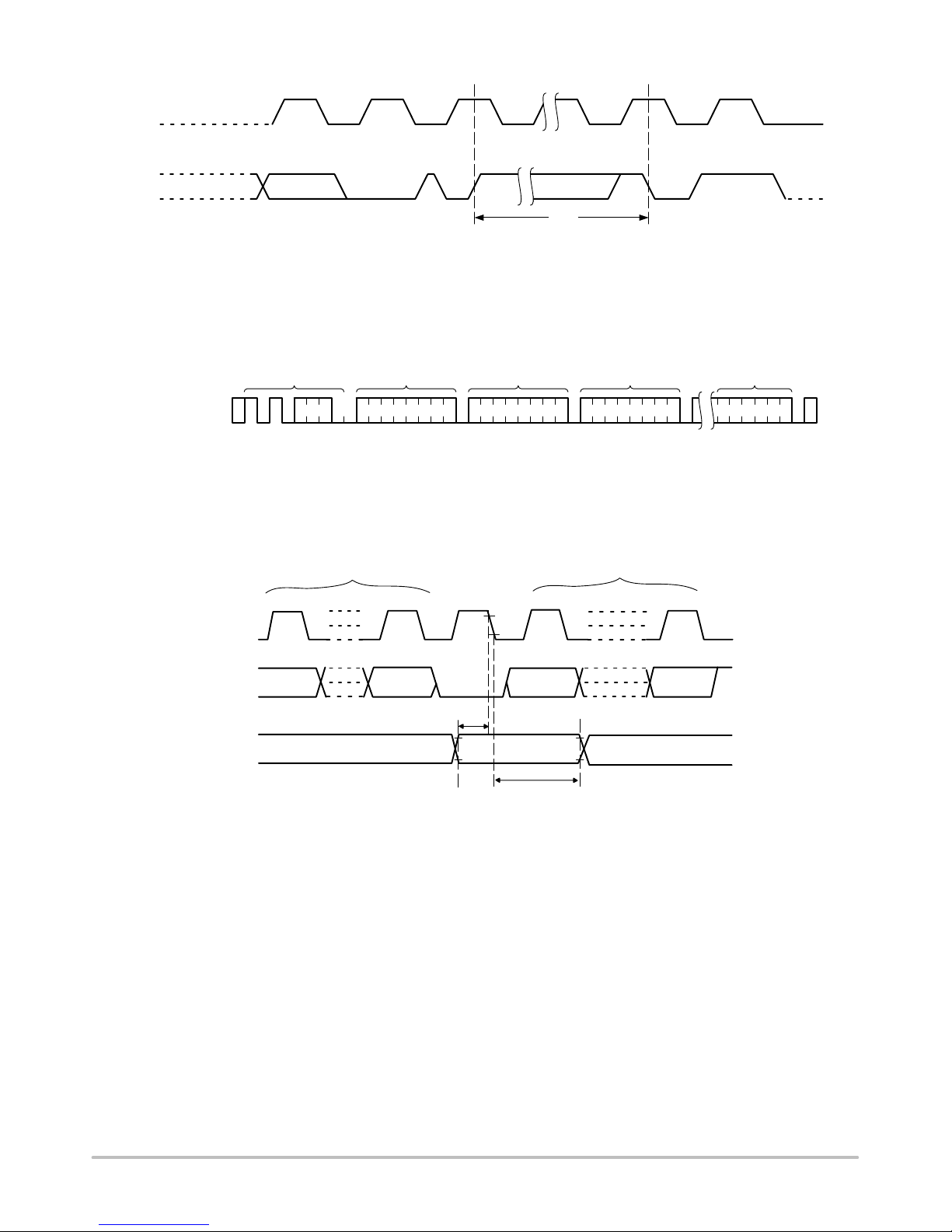
SCL
CAT24C01, CAT24C02, CAT24C04, CAT24C08, CAT24C16
SDA
BUS ACTIVITY:
MASTER
SLAVE
S
T
A
R
T
S
n = 1
P v 15
SCL
th
Bit
Byte n
ACK8
t
WR
STOP
CONDITION
START
CONDITION
Figure 7. Write Cycle Timing
SLAVE
ADDRESS
A
C
K
ADDRESS
BYTE
DATA
BYTE
n n+1 n+P
A
C
K
DATA
BYTE
A
C
K
A
C
K
DATA
BYTE
Figure 8. Page Write Sequence
ADDRESS
BYTE
1891 8
DATA
BYTE
ADDRESS
S
T
O
P
A
C
K
P
SDA
WP
a
7
a
0
t
SU:WP
d
t
HD:WP
7
d
0
Figure 9. WP Timing
http://onsemi.com
7
Page 8

CAT24C01, CAT24C02, CAT24C04, CAT24C08, CAT24C16
READ OPERATIONS
Immediate Read
Upon receiving a Slave address with the R/W bit set to ‘1’,
the CAT24Cxx will interpret this as a request for data
residing at the current byte address in memory. The
CAT24Cxx will acknowledge the Slave address, will
immediately shift out the data residing at the current address,
and will then wait for the Master to respond. If the Master
does not acknowledge the data (NoACK) and then follows
up with a STOP condition (Figure 10), the CAT24Cxx
returns to Standby mode.
Selective Read
Selective Read operations allow the Master device to
select at random any memory location for a read operation.
The Master device first performs a ‘dummy’ write operation
by sending the START condition, slave address and byte
address of the location it wishes to read. After the
BUS ACTIVITY:
MASTER
SLAVE
S
T
A
R
T
S
SLAVE
ADDRESS
CAT24Cxx acknowledges the byte address, the Master
device resends the START condition and the slave address,
this time with the R/W bit set to one. The CAT24Cxx then
responds with its acknowledge and sends the requested data
byte. The Master device does not acknowledge the data
(NoACK) but will generate a STOP condition (Figure 11).
Sequential Read
If during a Read session, the Master acknowledges the 1
data byte, then the CAT24Cxx will continue transmitting
data residing at subsequent locations until the Master
responds with a NoACK, followed by a STOP (Figure 12).
In contrast to Page Write, during Sequential Read the
address count will automatically increment to and then
wrap−around at end of memory (rather than end of page). In
the CAT24C01, the internal address count will not wrap
around at the end of the 128 byte memory space.
N
O
S
A
T
C
O
K
P
P
A
D ATA
C
BYTE
K
st
SCL
SDA 8
BUS ACTIVITY:
MASTER
SLAVE
BUS ACTIVITY:
MASTER
SLAVE
SLAVE
ADDRESS
89
th
Bit
Figure 10. Immediate Read Sequence and Timing
A
C
K
S
T
A
R
T
S
SLAVE
ADDRESS
S
T
A
SLAVE
R
T
S
A
C
K
ADDRESS
BYTEADDRESS
Figure 11. Selective Read Sequence
A
C
K
A
D ATA
C
BYTE
K
n
D ATA
BYTE
n+1
A
C
K
Figure 12. Sequential Read Sequence
D ATA
BYTE
n+2
STOPNO ACKDATA OUT
N
O
S
T
A
O
C
P
K
P
A
D ATA
C
BYTE
K
N
O
S
A
A
C
K
D ATA
BYTE
n+x
T
C
O
K
P
P
http://onsemi.com
8
Page 9

CAT24C01, CAT24C02, CAT24C04, CAT24C08, CAT24C16
PACKAGE DIMENSIONS
PDIP−8, 300 mils
CASE 646AA
ISSUE A
SYMBOL
A
A1
A2
b
E1
PIN # 1
IDENTIFICATION
D
TOP VIEW
A
A2
b2
c
D
E 7.62 8.25
E1
e
eB
L
MIN NOM MAX
5.33
0.38
2.92
0.36
1.14
0.20
9.02
6.10
7.87 10.92
2.92 3.80
3.30
0.46
1.52
0.25
9.27
7.87
6.35
2.54 BSC
3.30
E
4.95
0.56
1.78
0.36
10.16
7.11
L
eb
SIDE VIEW END VIEW
Notes:
(1) All dimensions are in millimeters.
(2) Complies with JEDEC MS-001.
b2
A1
c
eB
http://onsemi.com
9
Page 10

PIN # 1
IDENTIFICATION
CAT24C01, CAT24C02, CAT24C04, CAT24C08, CAT24C16
PACKAGE DIMENSIONS
SOIC 8, 150 mils
CASE 751BD
ISSUE O
SYMBOL MIN NOM MAX
1.35
0.10
0.33
0.19
4.80
5.80
3.80
1.27 BSC
0.25
0.40 1.27
0º 8º
E1 E
A
A1
b
c
D
E
E1
e
h
L
θ
1.75
0.25
0.51
0.25
5.00
6.20
4.00
0.50
TOP VIEW
D
A1
A
e
SIDE VIEW
Notes:
(1) All dimensions are in millimeters. Angles in degrees.
(2) Complies with JEDEC MS-012.
b
h
θ
c
L
END VIEW
http://onsemi.com
10
Page 11

CAT24C01, CAT24C02, CAT24C04, CAT24C08, CAT24C16
PACKAGE DIMENSIONS
TSSOP8, 4.4x3
b
E
E1
CASE 948AL
ISSUE O
SYMBOLθMIN NOM MAX
A1
A2
E1
L1
A
0.05
0.80
b
c
D
E
e
L
0.19
0.09
2.90
6.30
4.30
0.50
0.90
3.00
6.40
4.40
0.65 BSC
1.00 REF
0.60
1.20
0.15
1.05
0.30
0.20
3.10
6.50
4.50
0.75
0º 8º
e
TOP VIEW
D
A2
SIDE VIEW
Notes:
(1) All dimensions are in millimeters. Angles in degrees.
(2) Complies with JEDEC MO-153.
A
A1
q1
L1
c
L
END VIEW
http://onsemi.com
11
Page 12

CAT24C01, CAT24C02, CAT24C04, CAT24C08, CAT24C16
PACKAGE DIMENSIONS
MSOP 8, 3x3
CASE 846AD
ISSUE O
SYMBOL
A
A1
A2
b
c
E1E
D
E
E1
e
L
L1 0.95 REF
L2
θ
TOP VIEW
D
A2
A
MIN NOM MAX
1.10
0.05
0.75
0.22
0.13
2.90
4.80
2.90
0.40
0.10
0.85
3.00
4.90
3.00
0.65 BSC
0.60
0.25 BSC
0.15
0.95
0.38
0.23
3.10
5.00
3.10
0.80
0º 6º
DETAIL A
A1 e b
SIDE VIEW END VIEW
Notes:
(1) All dimensions are in millimeters. Angles in degrees.
(2) Complies with JEDEC MO-187.
c
q
L2
L
L1
DETAIL A
http://onsemi.com
12
Page 13

CAT24C01, CAT24C02, CAT24C04, CAT24C08, CAT24C16
N
PACKAGE DIMENSIONS
TDFN8, 2x3
CASE 511AK
ISSUE A
E
PIN#1 INDEX AREA
TOP VIEW SIDE VIEW BOTTOM VIEW
SYMBOL MIN NOM MAX
A 0.70 0.75 0.80
A1 0.00 0.02 0.05
A2 0.45 0.55 0.65
A3 0.20 REF
b 0.20 0.25 0.30
D 1.90 2.00 2.10
D2 1.30 1.40 1.50
E 3.00
E2 1.20 1.30 1.40
e
L 0.20 0.30 0.40
2.90
3.10
0.50 TYP
A
E2
A1
A2
ebD
D2
FRONT VIEW
PIN#1
IDENTIFICATIO
L
A3
Notes:
(1) All dimensions are in millimeters.
(2) Complies with JEDEC MO-229.
http://onsemi.com
13
Page 14

CAT24C01, CAT24C02, CAT24C04, CAT24C08, CAT24C16
PACKAGE DIMENSIONS
TSOT−23, 5 LEAD
CASE 419AE
ISSUE O
D
e
TOP VIEW
SYMBOLθMIN NOM MAX
E1 E
A1
A2
E1
L1
L2
A
0.01
0.80
b
c
D
E
e
L
0.30
0.12
0.30
0.05
0.87
0.15
2.90 BSC
2.80 BSC
1.60 BSC
0.95 TYP
0.40
0.60 REF
0.25 BSC
1.00
0.10
0.90
0.45
0.20
0.50
0º 8º
A2
A
b
A1
q
L
L1
c
L2
SIDE VIEW END VIEW
Notes:
(1) All dimensions are in millimeters. Angles in degrees.
(2) Complies with JEDEC MO-193.
http://onsemi.com
14
Page 15

CAT24C01, CAT24C02, CAT24C04, CAT24C08, CAT24C16
PACKAGE DIMENSIONS
TSOP−5
CASE 483−02
ISSUE H
NOTES:
1. DIMENSIONING AND TOLERANCING PER
NOTE 5
2X
2X
T0.10
T0.20
54
123
L
G
D
0.205XC AB
M
S
B
K
DETAIL Z
A
J
DETAIL Z
C
0.05
H
SEATING
PLANE
T
SOLDERING FOOTPRINT*
1.9
0.95
0.037
0.074
ASME Y14.5M, 1994.
2. CONTROLLING DIMENSION: MILLIMETERS.
3. MAXIMUM LEAD THICKNESS INCLUDES
LEAD FINISH THICKNESS. MINIMUM LEAD
THICKNESS IS THE MINIMUM THICKNESS
OF BASE MATERIAL.
4. DIMENSIONS A AND B DO NOT INCLUDE
MOLD FLASH, PROTRUSIONS, OR GATE
BURRS.
5. OPTIONAL CONSTRUCTION: AN
ADDITIONAL TRIMMED LEAD IS ALLOWED
IN THIS LOCATION. TRIMMED LEAD NOT TO
EXTEND MORE THAN 0.2 FROM BODY.
MILLIMETERS
DIM MIN MAX
A 3.00 BSC
B 1.50 BSC
C 0.90 1.10
D 0.25 0.50
G 0.95 BSC
H 0.01 0.10
J 0.10 0.26
K 0.20 0.60
L 1.25 1.55
M 0 10
__
S 2.50 3.00
2.4
0.094
1.0
0.039
0.7
0.028
SCALE 10:1
ǒ
inches
mm
*For additional information on our Pb−Free strategy and soldering
details, please download the ON Semiconductor Soldering and
Mounting Techniques Reference Manual, SOLDERRM/D.
Ǔ
http://onsemi.com
15
Page 16

CAT24C01, CAT24C02, CAT24C04, CAT24C08, CAT24C16
PACKAGE DIMENSIONS
UDFN8, 2x3 EXTENDED PAD
CASE 517AZ
ISSUE O
D
E
PIN #1 INDEX AREA
TOP VIEW SIDE VIEW
SYMBOL MIN NOM MAX
A 0.45 0.50 0.55
A1 0.00 0.02 0.05
A3 0.127 REF
b 0.20 0.25 0.30
D 1.95 2.00 2.05
D2 1.35 1.40 1.45
E 3.00
E2 1.25 1.30 1.35
e
L 0.25 0.30 0.35
2.95
3.05
0.50 REF
A
A1
0.065 REF
b
E2
BOTTOM VIEW
FRONT VIEW
D2
DETAIL A
e
L
DAP SIZE 1.8 x 1.8
PIN #1
IDENTIFICATION
A3
A
Notes:
(1) All dimensions are in millimeters.
(2) Refer JEDEC MO-236/MO-252.
http://onsemi.com
16
0.0 - 0.05A3
0.065 REF
Copper Exposed
DETAIL A
Page 17

CAT24C01, CAT24C02, CAT24C04, CAT24C08, CAT24C16
PACKAGE DIMENSIONS
WLCSP4, 0.84x0.86
CASE 567DC
ISSUE D
NOTE 5
REFERENCE
2X
2X
NOTE 4
M
0.10 BC
PIN A1
0.10 C
0.10 C
DETAIL A
0.10 C
0.05 C
4X
A
TOP VIEW
SIDE VIEW
b
B
A
12
BOTTOM VIEW
A2
NOTES:
1. DIMENSIONING AND TOLERANCING PER ASME
Y14.5M, 1994.
2. CONTROLLING DIMENSION: MILLIMETERS.
3. DATUM C, THE SEATING PLANE, IS DEFINED BY
THE SPHERICAL CROWNS OF THE CONTACT
BALLS.
4. COPLANARITY APPLIES TO SPHERICAL CROWNS
OF THE CONTACT BALLS.
5. DIMENSION b IS MEASURED AT THE MAXIMUM
CONTACT BALL DIAMETER PARALLEL TO DATUM C.
A
MILLIMETERS
DIMAMIN MAX
0.28
A1
0.08 0.12
A2 0.23 REF
A3* 0.025 REF
b 0.16 0.20
D 0.84 BSC
E
0.86 BSC
e 0.40 BSC
* Die Coat (Optional)
0.38
B
E
A
D
A3*
DETAIL A
A1
A2
* Die Coat
(Optional)
A
SEATING
C
PLANE
NOTE 3
RECOMMENDED
e
e
*For additional information on our Pb−Free strategy and soldering
details, please download the ON Semiconductor Soldering and
Mounting Techniques Reference Manual, SOLDERRM/D.
SOLDERING FOOTPRINT*
A1
0.40
PITCH
DIMENSIONS: MILLIMETERS
0.40
PITCH
PACKAGE
OUTLINE
4X
0.18
http://onsemi.com
17
Page 18

CAT24C01, CAT24C02, CAT24C04, CAT24C08, CAT24C16
PACKAGE DIMENSIONS
WLCSP5, 0.86x0.84
CASE 567DD
ISSUE C
NOTE 4
REFERENCE
2X
2X
5X
NOTE 3
M
0.10 BC
REFERENCE
PIN A1
0.10 C
0.10 C
0.10 C
0.05 C
5X
A
PIN A1
E
TOP VIEW
SIDE VIEW
b
C
B
A
13
BOTTOM VIEW
NOTES:
1. DIMENSIONING AND TOLERANCING PER ASME
Y14.5M, 1994.
2. CONTROLLING DIMENSION: MILLIMETERS.
3. DATUM C, THE SEATING PLANE, IS DEFINED BY THE
SPHERICAL CROWNS OF THE CONTACT BALLS.
4. COPLANARITY APPLIES TO SPHERICAL CROWNS
OF THE CONTACT BALLS.
5. DIMENSION b IS MEASURED AT THE MAXIMUM CONTACT BALL DIAMETER PARALLEL TO DATUM C.
MILLIMETERS
DIMAMIN MAX
0.29
A1
A2 0.23 REF
b 0.14 0.18
D 0.86 BSC
E
e 0.30 BSC
e1 0.52 BSC
0.39
0.10 0.14
0.84 BSC
A1
B
A
D
A
A2
SEATING
C
PLANE
RECOMMENDED
e
e1
2
*For additional information on our Pb−Free strategy and soldering
details, please download the ON Semiconductor Soldering and
Mounting Techniques Reference Manual, SOLDERRM/D.
SOLDERING FOOTPRINT*
0.30
PITCH
PACKAGE
OUTLINE
5X
A1
0.52
PITCH
DIMENSIONS: MILLIMETERS
0.16
http://onsemi.com
18
Page 19

CAT24C01, CAT24C02, CAT24C04, CAT24C08, CAT24C16
Ordering Information
CAT24C01 Ordering Information
Specific
Device Order Number
CAT24C01TDI−GT3 MM TSOT−23−5 Industrial NiPdAu Tape & Reel, 3,000 Units / Reel
CAT24C01VP2I−GT3* EE TDFN−8 Industrial NiPdAu Tape & Reel, 3,000 Units / Reel
CAT24C01WI−GT3 24C01WI SOIC−8 Industrial NiPdAu Tape & Reel, 3,000 Units / Reel
CAT24C01WE−GT3 24C01WI SOIC−8 Extended NiPdAu Tape & Reel, 3,000 Units / Reel
CAT24C01YI−GT3 C01 TSSOP−8 Industrial NiPdAu Tape & Reel, 3,000 Units / Reel
CAT24C01YE−GT3 C01 TSSOP−8 Extended NiPdAu Tape & Reel, 3,000 Units / Reel
CAT24C01ZI−GT3 ABMK MSOP−8 Industrial NiPdAu Tape & Reel, 3,000 Units / Reel
Device Marking
CAT24C02 Ordering Information (Notes 10, 11)
Specific
Device Order Number
CAT24C02WI−G 24C02H SOIC−8 Industrial NiPdAu Tube, 100 Units / Tube
CAT24C02WI−GA 24C02H SOIC−8 Industrial NiPdAu Tube, 100 Units / Tube
CAT24C02WI−GT3 24C02H SOIC−8 Industrial NiPdAu Tape & Reel, 3,000 Units / Reel
CAT24C02WI−GT3A 24C02H SOIC−8 Industrial NiPdAu Tape & Reel, 3,000 Units / Reel
CAT24C02WE−GT3 24C02H SOIC−8 Extended NiPdAu Tape & Reel, 3,000 Units / Reel
CAT24C02WE−GT3A 24C02H SOIC−8 Extended NiPdAu Tape & Reel, 3,000 Units / Reel
CAT24C02YI−G C02H TSSOP−8 Industrial NiPdAu Tube, 100 Units / Tube
CAT24C02YI−GA C02H TSSOP−8 Industrial NiPdAu Tube, 100 Units / Tube
CAT24C02YI−GT3 C02H TSSOP−8 Industrial NiPdAu Tape & Reel, 3,000 Units / Reel
CAT24C02YI−GT3A C02H TSSOP−8 Industrial NiPdAu Tape & Reel, 3,000 Units / Reel
CAT24C02YE−GT3 C02H TSSOP−8 Extended NiPdAu Tape & Reel, 3,000 Units / Reel
CAT24C02YE−GT3A C02H TSSOP−8 Extended NiPdAu Tape & Reel, 3,000 Units / Reel
CAT24C02VP2I−GT3* C1T TDFN−8 Industrial NiPdAu Tape & Reel, 3,000 Units / Reel
CAT24C02VP2IGT3A* C1T TDFN−8 Industrial NiPdAu Tape & Reel, 3,000 Units / Reel
CAT24C02VP2E−GT3* C1T TDFN−8 Extended NiPdAu Tape & Reel, 3,000 Units / Reel
CAT24C02VP2EGT3A* C1T TDFN−8 Extended NiPdAu Tape & Reel, 3,000 Units / Reel
CAT24C02ZI−GT3 C1 MSOP−8 Industrial NiPdAu Tape & Reel, 3,000 Units / Reel
CAT24C02ZE−GT3 C1 MSOP−8 Extended NiPdAu Tape & Reel, 3,000 Units / Reel
CAT24C02ZI−GT3A C1 MSOP−8 Industrial NiPdAu Tape & Reel, 3,000 Units / Reel
CAT24C02ZE−GT3A C1 MSOP−8 Extended NiPdAu Tape & Reel, 3,000 Units / Reel
CAT24C02TDI−GT3 C1 TSOT−23−5 Industrial NiPdAu Tape & Reel, 3,000 Units / Reel
CAT24C02TDE−GT3 C1 TSOT−23−5 Extended NiPdAu Tape & Reel, 3,000 Units / Reel
CAT24C02TDI−GT3A C1 TSOT−23−5 Industrial NiPdAu Tape & Reel, 3,000 Units / Reel
CAT24C02TDE−GT3A C1 TSOT−23−5 Extended NiPdAu Tape & Reel, 3,000 Units / Reel
CAT24C02LI−GA 24C02H PDIP−8 Industrial NiPdAu Tube, 50 Units / Tube
CAT24C02LE−GA 24C02H PDIP−8 Extended NiPdAu Tube, 50 Units / Tube
CAT24C02HU4IGT3A C1U UDFN8−EP Industrial NiPdAu Tape & Reel, 3,000 Units / Reel
CAT24C02HU4EGT3A C1U UDFN8−EP Extended NiPdAu Tape & Reel, 3,000 Units / Reel
CAT24C02TSI−T3 C1 TSOP−5 Industrial Matte−Tin Tape & Reel, 3,000 Units / Reel
9. Industrial temperature range is −40°C to +85°C and Extended temperature range is −40°C to +125°C.
10.Part numbers ending with “A” for the CAT24C02 are for Gresham (Product Rev H) only die.
11. The CAT24C02 ”non−A” Device Order Numbers use Gresham die (Rev H) for date codes, starting August 1st, 2012. Therefore the Specific
Device Marking for these OPNs reflect Rev H die.
* The TDFN (VP2) package is not recommended for new designs.
Device Marking
Package
Type
Package
Type
Temperature
Range (Note 9)
Temperature
Range (Note 9)
Lead
Finish
Lead
Finish
Shipping
Shipping
http://onsemi.com
19
Page 20

CAT24C01, CAT24C02, CAT24C04, CAT24C08, CAT24C16
CAT24C04 Ordering Information
Specific
Device Order Number
CAT24C04WI−G 24C04K SOIC−8 Industrial NiPdAu Tube, 100 Units / Tube
CAT24C04WI−GT3 24C04K SOIC−8 Industrial NiPdAu Tape & Reel, 3,000 Units / Reel
CAT24C04WE−GT3 24C04K SOIC−8 Extended NiPdAu Tape & Reel, 3,000 Units / Reel
CAT24C04YI−G C04K TSSOP−8 Industrial NiPdAu Tube, 100 Units / Tube
CAT24C04YI−GT3 C04K TSSOP−8 Industrial NiPdAu Tape & Reel, 3,000 Units / Reel
CAT24C04YE−GT3 C04 TSSOP−8 Extended NiPdAu Tape & Reel, 3,000 Units / Reel
CAT24C04VP2I−GT3* C2T TDFN−8 Industrial NiPdAu Tape & Reel, 3,000 Units / Reel
CAT24C04LI−G 24C04K PDIP−8 Industrial NiPdAu Tube, 50 Units / Tube
CAT24C04LE−G 24C04K PDIP−8 Extended NiPdAu Tube, 50 Units / Tube
CAT24C04ZI−GT3 C2 MSOP−8 Industrial NiPdAu Tape & Reel, 3,000 Units / Reel
CAT24C04ZE−GT3 C2 MSOP−8 Extended NiPdAu Tape & Reel, 3,000 Units / Reel
CAT24C04C4ATR 4 WLCSP−4 Industrial N/A Tape & Reel, 5,000 Units / Reel
CAT24C04C5ATR 4 WLCSP−5 Industrial N/A Tape & Reel, 5,000 Units / Reel
CAT24C04TDI−GT3 C2 TSOT−23−5 Industrial NiPdAu Tape & Reel, 3,000 Units / Reel
CAT24C04TDE−GT3 C2 TSOT−23−5 Extended NiPdAu Tape & Reel, 3,000 Units / Reel
CAT24C04HU4I−GT3 C2U UDFN8−EP Industrial NiPdAu Tape & Reel, 3,000 Units / Reel
CAT24C04HU4E−GT3 C2U UDFN8−EP Extended NiPdAu Tape & Reel, 3,000 Units / Reel
Device Marking
Package
Type
Temperature
Range (Note 12)
Lead
Finish
Shipping
CAT24C08 Ordering Information
Specific
Device Order Number
CAT24C08WI−G 24C08K SOIC−8 Industrial NiPdAu Tube, 100 Units / Tube
CAT24C08WI−GT3 24C08K SOIC−8 Industrial NiPdAu Tape & Reel, 3,000 Units / Reel
CAT24C08WE−GT3 24C08K SOIC−8 Extended NiPdAu Tape & Reel, 3,000 Units / Reel
CAT24C08YI−G C08K TSSOP−8 Industrial NiPdAu Tube, 100 Units / Tube
CAT24C08YI−GT3 C08K TSSOP−8 Industrial NiPdAu Tape & Reel, 3,000 Units / Reel
CAT24C08YE−GT3 C08 TSSOP−8 Extended NiPdAu Tape & Reel, 3,000 Units / Reel
CAT24C08VP2I−GT3* C3T TDFN−8 Industrial NiPdAu Tape & Reel, 3,000 Units / Reel
CAT24C08VP2E−GT3* C3T TDFN−8 Extended NiPdAu Tape & Reel, 3,000 Units / Reel
CAT24C08LI−G 24C08K PDIP−8 Industrial NiPdAu Tube, 50 Units / Tube
CAT24C08LE−G 24C08K PDIP−8 Extended NiPdAu Tube, 50 Units / Tube
CAT24C08ZI−GT3 C3 MSOP−8 Industrial NiPdAu Tape & Reel, 3,000 Units / Reel
CAT24C08ZE−GT3 C3 MSOP−8 Extended NiPdAu Tape & Reel, 3,000 Units / Reel
CAT24C08C4ATR 8 WLCSP−4 Industrial N/A Tape & Reel, 5,000 Units / Reel
CAT24C08C4CTR** 8 WLCSP−4 Industrial N/A Tape & Reel, 5,000 Units / Reel
CAT24C08C5ATR 8 WLCSP−5 Industrial N/A Tape & Reel, 5,000 Units / Reel
CAT24C08TDI−GT3 C3 TSOT−23−5 Industrial NiPdAu Tape & Reel, 3,000 Units / Reel
CAT24C08TDE−GT3 C3 TSOT−23−5 Extended NiPdAu Tape & Reel, 3,000 Units / Reel
CAT24C08HU4I−GT3 C3U UDFN8−EP Industrial NiPdAu Tape & Reel, 3,000 Units / Reel
CAT24C08HU4E−GT3 C3U UDFN8−EP Extended NiPdAu Tape & Reel, 3,000 Units / Reel
12.Industrial temperature range is −40°C to +85°C and Extended temperature range is −40°C to +125°C.
* The TDFN (VP2) package is not recommended for new designs.
** CAT24C08C4CTR is a backside coated version. Contact factory for other densities.
Device Marking
Package
Type
Temperature
Range (Note 12)
Lead
Finish
Shipping
http://onsemi.com
20
Page 21

CAT24C01, CAT24C02, CAT24C04, CAT24C08, CAT24C16
CAT24C16 Ordering Information
Specific
Device Order Number
Device Marking
CAT24C16WI−G 24C16K SOIC−8 Industrial NiPdAu Tube, 100 Units / Tube
CAT24C16WI−GT3 24C16K SOIC−8 Industrial NiPdAu Tape & Reel, 3,000 Units / Reel
CAT24C16WE−GT3 24C16K SOIC−8 Extended NiPdAu Tape & Reel, 3,000 Units / Reel
CAT24C16YI−G C16K TSSOP−8 Industrial NiPdAu Tube, 100 Units / Tube
CAT24C16YI−GT3 C16K TSSOP−8 Industrial NiPdAu Tape & Reel, 3,000 Units / Reel
CAT24C16YE−GT3 C16 TSSOP−8 Extended NiPdAu Tape & Reel, 3,000 Units / Reel
CAT24C16VP2I−GT3* C4T TDFN−8 Industrial NiPdAu Tape & Reel, 3,000 Units / Reel
CAT24C16VP2E−GT3* C4T TDFN−8 Extended NiPdAu Tape & Reel, 3,000 Units / Reel
CAT24C16LI−G 24C16K PDIP−8 Industrial NiPdAu Tube, 50 Units / Tube
CAT24C16LE−G 24C16K PDIP−8 Extended NiPdAu Tube, 50 Units / Tube
CAT24C16ZI−GT3 C4 MSOP−8 Industrial NiPdAu Tape & Reel, 3,000 Units / Reel
CAT24C16ZE−GT3 C4 MSOP−8 Extended NiPdAu Tape & Reel, 3,000 Units / Reel
CAT24C16C4ATR 6 WLCSP−4 Industrial N/A Tape & Reel, 5,000 Units / Reel
CAT24C16C5ATR 6 WLCSP−5 Industrial N/A Tape & Reel, 5,000 Units / Reel
CAT24C16TDI−GT3 C4 TSOT−23−5 Industrial NiPdAu Tape & Reel, 3,000 Units / Reel
CAT24C16TDE−GT3 C4 TSOT−23−5 Extended NiPdAu Tape & Reel, 3,000 Units / Reel
CAT24C16HU4I−GT3 C4U UDFN8−EP Extended NiPdAu Tape & Reel, 3,000 Units / Reel
13.Industrial temperature range is −40°C to +85°C and Extended temperature range is −40°C to +125°C.
14.All packages are RoHS−compliant (Lead−free, Halogen−free).
15.For information on tape and reel specifications, including part orientation and tape sizes, please refer to our Tape and Reel Packaging
Specifications Brochure, BRD8011/D.
16.For detailed information and a breakdown of device nomenclature and numbering systems, please see the ON Semiconductor Device
Nomenclature document, TND310/D, available at www.onsemi.com
* The TDFN (VP2) package is not recommended for new designs.
Package
Type
Temperature
Range (Note 13)
Lead
Finish
Shipping
ON Semiconductor is licensed by Philips Corporation to carry the I2C Bus Protocol.
ON Semiconductor and are registered trademarks of Semiconductor Components Industries, LLC (SCILLC). SCILLC owns the rights to a number of patents, trademarks,
copyrights, trade secrets, and other intellectual property. A listing of SCILLC’s product/patent coverage may be accessed at www.onsemi.com/site/pdf/Patent−Marking.pdf. SCILLC
reserves the right to make changes without further notice to any products herein. SCILLC makes no warranty, representation or guarantee regarding the suitability of its products for any
particular purpose, nor does SCILLC assume any liability arising out of the application or use of any product or circuit, and specifically disclaims any and all liability, including without
limitation special, consequential or incidental damages. “Typical” parameters which may be provided in SCILLC data sheets and/or specifications can and do vary in different applications
and actual performance may vary over time. All operating parameters, including “Typicals” must be validated for each customer application by customer’s technical experts. SCILLC
does not convey any license under its patent rights nor the rights of others. SCILLC products are not designed, intended, or authorized for use as components in systems intended for
surgical implant into the body, or other applications intended to support or sustain life, or for any other application in which the failure of the SCILLC product could create a situation where
personal injury or death may occur. Should Buyer purchase or use SCILLC products for any such unintended or unauthorized application, Buyer shall indemnify and hold SCILLC and
its officers, employees, subsidiaries, affiliates, and distributors harmless against all claims, costs, damages, and expenses, and reasonable attorney fees arising out of, directly or indirectly,
any claim of personal injury or death associated with such unintended or unauthorized use, even if such claim alleges that SCILLC was negligent regarding the design or manufacture
of the part. SCILLC is an Equal Opportunity/Affirmative Action Employer. This literature is subject to all applicable copyright laws and is not for resale in any manner.
PUBLICATION ORDERING INFORMATION
LITERATURE FULFILLMENT:
Literature Distribution Center for ON Semiconductor
P.O. Box 5163, Denver, Colorado 80217 USA
Phone: 303−675−2175 or 800−344−3860 Toll Free USA/Canada
Fax: 303−675−2176 or 800−344−3867 Toll Free USA/Canada
Email: orderlit@onsemi.com
N. American Technical Support: 800−282−9855 Toll Free
USA/Canada
Europe, Middle East and Africa Technical Support:
Phone: 421 33 790 2910
Japan Customer Focus Center
Phone: 81−3−5817−1050
http://onsemi.com
21
ON Semiconductor Website: www.onsemi.com
Order Literature: http://www.onsemi.com/orderlit
For additional information, please contact your local
Sales Representative
CAT24C01/D
 Loading...