

Page 1
BR262PMEVK
BELASIGNA) R262
Prototyping Module
Evaluation Board
User'sManual
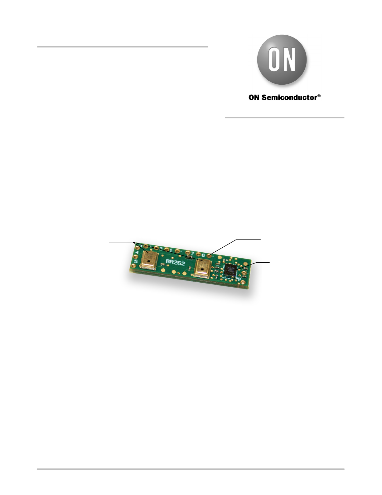
The BelaSigna R262 Prototyping Module
The BelaSigna R262 prototyping module is a miniature,
self-contained unit that can be integrated into a product or
prototype to evaluate the performance of BelaSigna R262
“in-form-factor”.
Key Features
The module is shown in Figure 1 and features:
A Miniature Size of only 22 mm 6mm
The 30-ball WLCSP Version of BelaSigna R262
(BR262W30A103E1G)
http://onsemi.com
EVAL BOARD USER’S MANUAL
Two MEMS Microphones Spaced 10 mm Apart
(Knowles Part Number SPU0410HR5H−PB)
Through-hole Test Points for External Connections
Configured to Boot Directly to the ROM Application
Using the Internal Clock
2
I
C and GPIO Signals Available on Test Points
An Onboard I
Application
2
C EEPROM for Optional Custom
Dual MEMS
Microphones
Figure 1. BelaSigna R262 Prototyping Module
Default Configuration
The prototyping module configures BelaSigna R262 to
run off its internal oscillator and to boot directly into the
ROM-based noise reduction algorithm. The module is
pre-configured to simultaneously output two different
algorithm turnings: a pure close-talk output on AO0, and an
output that is close-talk mixed 60% towards far-talk on
AO1. All that is required is to supply the module with 1.8 to
Through-hole Test
points
BelaSigna R262
3.3 VDC (requires approximately 20 mA), and to connect
the analog outputs to your in-form-factor design. Power is
connected to VBAT (+) and GND (−). The prototyping
module configures the ROM application as summarized in
Table 1 when power is applied.
A description of all test points and a complete schematic
and layout is available in Appendix A.
Semiconductor Components Industries, LLC, 2012
December, 2012 − Rev. 0
1 Publication Order Number:
EVBUM2166/D
Page 2
BR262PMEVK
Table 1. BelaSigna R262 PROTOTYPING MODULE LSAD CONFIGURATION
Pin Name Preset Description
CLOCK_SEL (SPI_CLK/GPIO0) 7 Internal Clock
BOOT_SEL (SPI_CS/GPIO1) 4 Active Mode
CHAN_SEL (SPI_SERO/GPIO2) 3 Dual Output Noise Reduction
ALPHA_SEL (SPI_SERI/GPIO3) 4 Mixer set 60% between Start and End of Range
Talk Distance Selectable between Close-talk and Far-talk
(5 cm – 500 cm)
(Two Single-ended Analog Outputs)
Channel 0 as per BOOT_SEL “Start of Range” (Close-talk)
Channel 1 as per BOOT_SEL and ALPHA_SEL
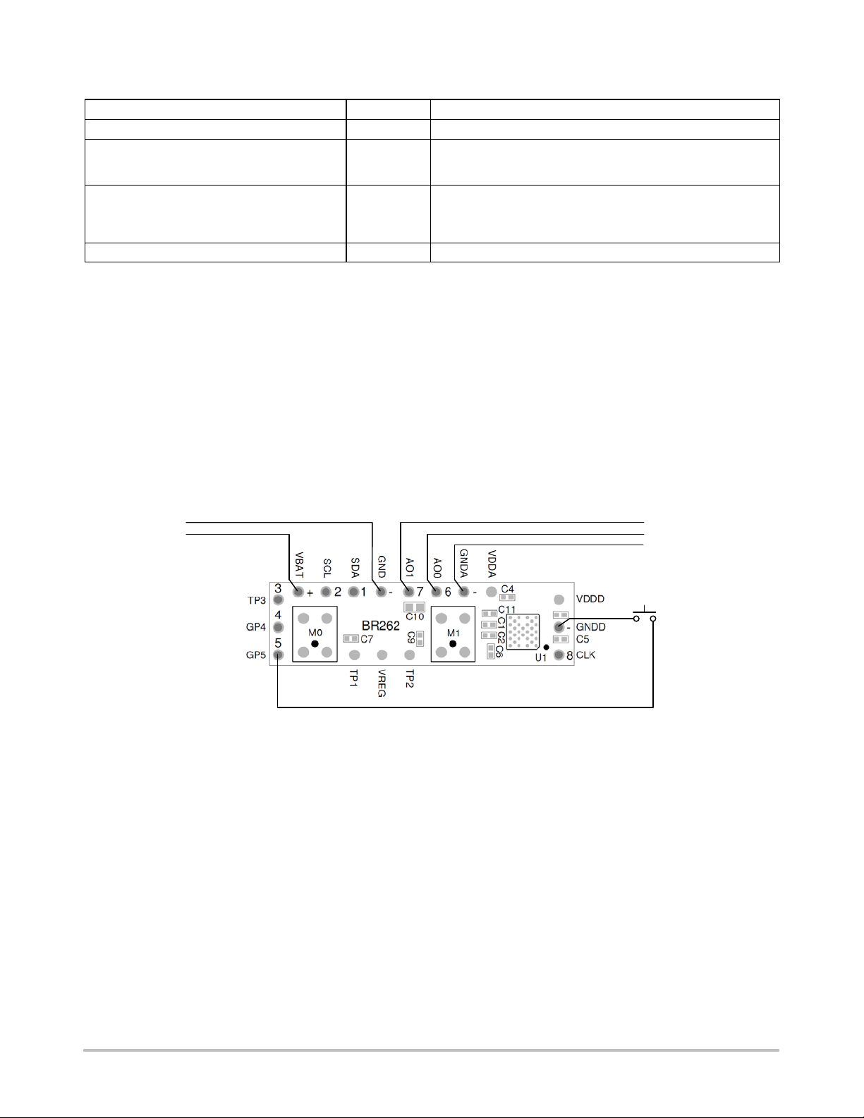
Connecting the Prototyping Module
The analog output signals are available on AO0 (6),
AO1 (7), and GNDA (−). An optional momentary
push-button control can be connected between GP5 (5) and
GNDD (−) that can be used to swap the two processed
outputs between AO0 and AO1. The pinout for the module,
along with typical connections are illustrated in Figure 2.
The analog outputs of the device can be connected to your
system’s analog inputs as single-ended signals using AO0
and GNDA and/or AO1 and GNDA. If the module is
re-configured to output a mono, differential analog output
by changing the CHAN_SEL resistors R4 and R5, via I
2
commands, or by loading a custom application, you can
GND
1.8 to 3.3 VDC
connect AO0 and AO1 to your system as a differential
analog signal.
NOTE: The analog output impedance is 3 kW and is intended to drive
a high-impedance (line-level) input, not speakers nor
headphones directly. Refer to the BelaSigna R262 datasheet
for more information on output stage characteristics.
You can also use the prototyping module as a digital
microphone replacement outputting a stereo DMIC signal
on test point GP4 (4), provided you supply an appropriate
DMIC clock signal on the CLK (8) test point and
re-configure the module’s CLOCK_SEL resistive divider to
C
match the provided clock frequency. Refer to the
BelaSigna R262 datasheet for more information.
Analog Output 1
Analog Output 0
Analog GND
Swap Channels
Figure 2. BelaSigna R262 Prototyping Module Typical Connections
Operating the Prototyping Module
The default configuration of the prototyping module
provides the widest noise reduction adjustment range
(close-talk to far-talk) by selecting preset 4 on the
BOOT_SEL input, and is pre-configured to simultaneously
output two different algorithm tunings: a pure close-talk
output on AO0, and an output that is close-talk mixed 60%
towards far-talk on AO1. The processed outputs from these
two algorithm tunings are available as single-ended analog
outputs on AO0 – GNDA, and AO1 – GNDA. The
application will swap the output channels when GP5 is
momentarily pulled low. If a momentary push-button is
connected between GP5 and GNDD, pressing and releasing
http://onsemi.com
this button will swap the two processed outputs between
AO0 and AO1.
Close-Talk
Close-talk mode aggressively filters noise and manages
gain to pick up speech within 5 to 10 cm from the
microphone array, effectively attenuating both speech and
noise that is farther away. This mode is suitable for mobile
handsets and radios where the speech source is very close to
the microphones and the noise level can be quite high; up to
90 dB SPL. Noise reduction performance in this mode
ranges from 20 to 30 dB SNR improvement (SNR−I),
depending on the type of noise.
2
Page 3

BR262PMEVK
Close-Talk Mixed 60% Towards Far-Talk
The second, mixed mode of close-talk mixed 60%
towards far-talk is similar to the core near-talk mode and
features excellent noise reduction in applications where the
speech source is located slightly further away from the
microphones; typically 50 to 100 cm. This mode is suitable
for handsfree devices and performs well in noise levels up
to 70 dB SPL. Expected noise reduction performance in this
mode is 10 to 20 dB SNR−I, depending on the type of noise.
Refer to the AND9109/D − BelaSigna R262 Getting
Started Guide for details on the different algorithm modes
and performance metrics.
Module Positioning
The speech source can come from any direction (normally
in front of the microphones), as long as it is within the
“working sphere” of the current algorithm mode. For
close-talk mode, the mouth reference point (MRP) should be
located between 5 and 10 cm from the microphones.
For close-talk mixed 60% towards far-talk, the MRP
should be located between 50 and 100 cm from the
microphones.
Acoustic Design
If the prototyping module is replacing an existing
microphone, the old microphone should be removed and the
module should be mounted as close as possible to the
original microphone location.
The device casing should be modified or manufactured
such that there is an appropriate acoustic path to the two
microphones on the module. Two holes roughly 0.5 to 1 mm
in diameter should be drilled in the casing 10 mm apart
above the sound ports of the onboard microphones. If
possible a rubber or foam isolation gasket should be installed
between the microphones and the device casing.
Electrical Considerations
The analog output(s) of the module can be connected
directly to any existing microphone input but keep in mind
that it may be necessary to lower any existing microphone
pre-amplification.
Care should be taken to properly shield the module and the
analog outputs if your product involves radio frequencies.
Use coaxial or shielded cable when connecting the analog
outputs of the module, and if necessary, wrap the module
with foil tape.
Customizing the Prototyping Module
If you would prefer to have the default tunings to be
something other than close-talk and close-talk mixed 60%
towards far-talk, you can change the values of the resistive
dividers on the BOOT_SEL (R3 and R4) and ALPHA_SEL
(R7 and R8) inputs. A component placement diagram
showing the locations of the various resistors is illustrated in
Figure 3. Refer to the BelaSigna R262 datasheet for more
information on BOOT_SEL and ALPHA_SEL inputs, and
the resistive divider values required to achieve specific
presets.
If you would like to re-configure the module to use the
DMIC interface, you must supply an appropriate DMIC
clock signal on the CLK test point and re-configure the
module’s CLOCK_SEL resistive divider (R1 and R2) to
match the provided clock frequency. A stereo DMIC signal
will be output on test point GP4. Refer to the
BelaSigna R262 datasheet for more information on the
supported DMIC clock frequencies, and the resistive divider
values required to select them.
If you would like to re-configure the module to output a
differential analog signal, you must adjust the resistive
dividers on the CHAN_SEL input (R5 and R6) to select
preset 0 or preset 5. Refer to the BelaSigna R262 datasheet
for more information on the CHAN_SEL input and the
resistive divider values required to achieve specific presets.
If you would like to re-configure the module to load a
custom application from the EEPROM, you must load a
valid custom application onto the EEPROM and remove
resistor R4 to have the module boot from EEPROM. Refer
to the BelaSigna R262 datasheet for more information on the
BOOT_SEL input and the resistive divider values required
to achieve specific presets. Contact your local
ON Semiconductor support representative for more
information about custom applications.
http://onsemi.com
3
Page 4

BR262PMEVK
APPENDIX A
For your convenience, the prototyping module has many
test points. Signals that are intended to be interfaced to
external devices are provided on through-hole test points.
All of the available test points are summarized in Table 2.
Table 2. BelaSigna R262 PROTOTYPING MODULE TEST POINT DESCRIPTIONS
Test Point Name Designator Description
VBAT + Main Module Power Supply (1.8 to 3.3 VDC, 20 mA)
SCL 2 I2C Clock
SDA 1 I2C Data
GND − Main Module Ground
AO1 7 Channel 1 Analog Output
AO0 6 Channel 0 Analog Output
GNDA − Analog Ground (Internally Connected to GND)
VDDA Internal 2.0 V Power Supply
VDDD Digital Power Supply (Internally Generated)
GNDD − Digital Ground (Internally Connected to GND)
CLK 8 Optional Input Clock
TP2 Microphone 1 Test Point
VREG Internal 1.0 V Power Supply
TP1 Microphone 0 Test Point
GP5 5 Optional GPIO Input (SWAP_CHAN)
GP4 4 Optional DMIC Output
TP3 3 Reset
Figure 3. Component Placement Diagram
http://onsemi.com
4
Page 5

BR262PMEVK
Figure 4. BelaSigna R262 Prototyping Module Schematic
http://onsemi.com
5
Page 6

BR262PMEVK
Figure 5. BelaSigna R262 Prototyping Module Layout
(View from Top to Bottom)
Company or Product Inquiries
For more information about ON Semiconductor products
or services visit our Web site at www.onsemi.com
BELASIGNA is a registered trademark of Semiconductor Components Industries, LLC (SCILLC).
ON Semiconductor and are registered trademarks of Semiconductor Components Industries, LLC (SCILLC). SCILLC owns the rights to a number of patents, trademarks,
copyrights, trade secrets, and other intellectual property. A listing of SCILLC’s product/patent coverage may be accessed at www.onsemi.com/site/pdf/Patent−Marking.pdf. SCILLC
reserves the right to make changes without further notice to any products herein. SCILLC makes no warranty, representation or guarantee regarding the suitability of its products for any
particular purpose, nor does SCILLC assume any liability arising out of the application or use of any product or circuit, and specifically disclaims any and all liability, including without
limitation special, consequential or incidental damages. “Typical” parameters which may be provided in SCILLC data sheets and/or specifications can and do vary in different applications
and actual performance may vary over time. All operating parameters, including “Typicals” must be validated for each customer application by customer’s technical experts. SCILLC
does not convey any license under its patent rights nor the rights of others. SCILLC products are not designed, intended, or authorized for use as components in systems intended for
surgical implant into the body, or other applications intended to support or sustain life, or for any other application in which the failure of the SCILLC product could create a situation where
personal injury or death may occur. Should Buyer purchase or use SCILLC products for any such unintended or unauthorized application, Buyer shall indemnify and hold SCILLC and
its officers, employees, subsidiaries, affiliates, and distributors harmless against all claims, costs, damages, and expenses, and reasonable attorney fees arising out of, directly or indirectly,
any claim of personal injury or death associated with such unintended or unauthorized use, even if such claim alleges that SCILLC was negligent regarding the design or manufacture
of the part. SCILLC is an Equal Opportunity/Affirmative Action Employer. This literature is subject to all applicable copyright laws and is not for resale in any manner.
PUBLICATION ORDERING INFORMATION
LITERATURE FULFILLMENT:
Literature Distribution Center for ON Semiconductor
P.O. Box 5163, Denver, Colorado 80217 USA
Phone: 303−675−2175 or 800−344−3860 Toll Free USA/Canada
Fax: 303−675−2176 or 800−344−3867 Toll Free USA/Canada
Email: orderlit@onsemi.com
.
N. American Technical Support: 800−282−9855 Toll Free
USA/Canada
Europe, Middle East and Africa Technical Support:
Phone: 421 33 790 2910
Japan Customer Focus Center
Phone: 81−3−5817−1050
http://onsemi.com
Technical Contact Information
For technical support, email: dsp.support@onsemi.com
ON Semiconductor Website: www.onsemi.com
Order Literature: http://www.onsemi.com/orderlit
For additional information, please contact your local
Sales Representative
EVBUM2166/D
6
 Loading...