

Page 1
BCP53 Series
PNP Silicon
Epitaxial Transistors
This PNP Silicon Epitaxial transistor is designed for use in audio
amplifier applications. The device is housed in the SOT‐223 package
which is designed for medium power surface mount applications.
•High Current: 1.5 Amps
•NPN Complement is BCP56
•The SOT‐223 Package can be soldered using wave or reflow. The
formed leads absorb thermal stress during soldering, eliminating the
possibility of damage to the die
•Device Marking:
BCP53T1 = AH
BCP53-10T1 = AH-10
BCP53-16T1 = AH-16
•Pb-Free Packages are Available
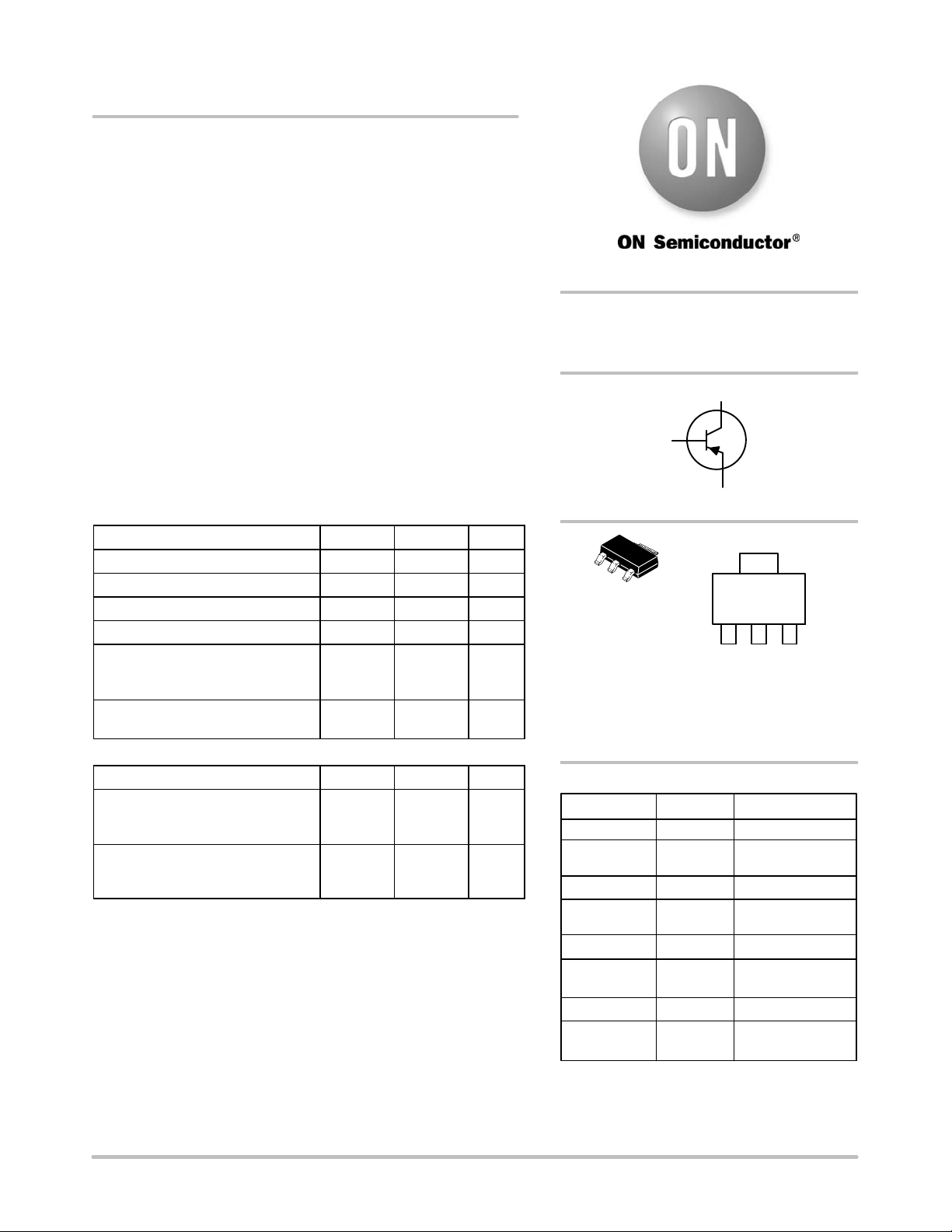
http://onsemi.com
MEDIUM POWER HIGH
CURRENT SURFACE MOUNT
PNP TRANSISTORS
COLLECTOR 2,4
BASE
1
MAXIMUM RATINGS (T
Rating Symbol Value Unit
Collector‐Emitter Voltage V
Collector‐Base Voltage V
Emitter‐Base Voltage V
Collector Current I
Total Power Dissipation
@ TA = 25°C (Note 1.)
Derate above 25°C
Operating and Storage
Temperature Range
= 25°C unless otherwise noted)
C
CEO
CBO
EBO
C
P
D
TJ, T
stg
-80 Vdc
-100 Vdc
-5.0 Vdc
1.5 Adc
1.5
12
-65 to
+150
Watts
mW/°C
°C
THERMAL CHARACTERISTICS
Characteristic Symbol Max Unit
Thermal Resistance,
Junction to Ambient
(surface mounted)
Lead Temperature for Soldering,
0.0625″ from case
Time in Solder Bath
Stresses exceeding Maximum Ratings may damage the device. Maximum
Ratings are stress ratings only. Functional operation above the Recommended
Operating Conditions is not implied. Extended exposure to stresses above the
Recommended Operating Conditions may affect device reliability.
1. Device mounted on a glass epoxy printed circuit board 1.575 in. x 1.575 in.
x 0.059 in.; mounting pad for the collector lead min. 0.93 sq. in.
R
θ
JA
T
L
83.3 °C/W
260
10
°C
Sec
EMITTER 3
MARKING DIAGRAM
4
1
2
3
SOT-223
CASE 318E
STYLE 1
A = Assembly Location
Y = Year
W = Work Week
XXXXX = Specific Device Code
G = Pb-Free Package
(Note: Microdot may be in either location)
AYW
XXXXXG
G
1
ORDERING INFORMATION
Device Package Shipping
BCP53T1 SOT-223
BCP53T1G SOT-223
(Pb-Free)
BCP53-10T1 SOT-223 1000/Tape & Reel
BCP53-10T1G SOT-223
(Pb-Free)
BCP53-16T1 SOT-223 1000/Tape & Reel
BCP53-16T1G SOT-223
(Pb-Free)
BCP53-16T3 SOT-223 4000/Tape & Reel
BCP53-16T3G SOT-223
(Pb-Free)
†For information on tape and reel specifications,
including part orientation and tape sizes, please
refer to our Tape and Reel Packaging Specifications
Brochure, BRD8011/D.
1000/Tape & Reel
1000/Tape & Reel
1000/Tape & Reel
1000/Tape & Reel
4000/Tape & Reel
†
© Semiconductor Components Industries, LLC, 2008
February, 2008 - Rev. 6
1 Publication Order Number:
BCP53T1/D
Page 2
BCP53 Series
ELECTRICAL CHARACTERISTICS (T
= 25°C unless otherwise noted)
A
Characteristics Symbol Min Typ Max Unit
OFF CHARACTERISTICS
Collector‐Base Breakdown Voltage (IC = -100 μAdc, IE = 0) V
Collector‐Emitter Breakdown Voltage (IC = -1.0 mAdc, IB = 0) V
Collector‐Emitter Breakdown Voltage (IC = -100 μAdc, RBE = 1.0 kohm) V
Emitter‐Base Breakdown Voltage (IE = -10 μAdc, IC = 0) V
Collector‐Base Cutoff Current (VCB = -30 Vdc, IE = 0) I
Emitter‐Base Cutoff Current (VEB = -5.0 Vdc, IC = 0) I
ON CHARACTERISTICS
DC Current Gain (IC = -5.0 mAdc, VCE = -2.0 Vdc) All Part Types
(IC = -150 mAdc, VCE = -2.0 Vdc) BCP53
BCP53-10
BCP53-16
(IC = -500 mAdc, VCE = -2.0 Vdc) All Part Types
Collector‐Emitter Saturation Voltage (IC = -500 mAdc, IB = -50 mAdc) V
Base‐Emitter On Voltage (IC = -500 mAdc, VCE = -2.0 Vdc) V
DYNAMIC CHARACTERISTICS
Current‐Gain - Bandwidth Product
(IC = -10 mAdc, VCE = -5.0 Vdc, f = 35 MHz)
(BR)CBO
(BR)CEO
(BR)CER
(BR)EBO
CBO
EBO
h
FE
CE(sat)
BE(on)
f
T
-100 - - Vdc
-80 - - Vdc
-100 - - Vdc
-5.0 - - Vdc
- - -100 nAdc
- - -10 μAdc
25
40
63
100
25
-
-
-
-
-
250
160
250
-
-
- - -0.5 Vdc
- - -1.0 Vdc
- 50 - MHz
http://onsemi.com
2
Page 3

BCP53 Series
TYPICAL CHARACTERISTICS
2.0
IC/IB = 10 BCP53, -10, -16
1.8
1.6
1.4
1.2
1.0
0.8
0.6
, COLLECTOR EMITTER
0.4
SATURATION VOLTAGE (V)
ce(sat)
V
0.2
0
IC, COLLECTOR CURRENT (mA) IC, COLLECTOR CURRENT (A)
+150°C
Figure 1. Collector Emitter Saturation Voltage
vs. Collector Current
180
160
140
120
100
80
60
, DC CURRENT GAIN
FE
40
h
20
0
IC, COLLECTOR CURRENT (A) IC, COLLECTOR CURRENT (A)
150°C, 2 V
25°C, 5 V
25°C, 2 V
-55°C, 5 V
-55°C, 2 V
150°C, 5 V
Figure 3. DC Current Gain vs. Collector
Current (BCP53-10)
-55°C
+25°C
200
180
160
140
120
100
80
60
, DC CURRENT GAIN
FE
h
40
20
1010.10.010.001
300
250
200
150
100
, DC CURRENT GAIN
FE
h
50
1010.10.010.001
150°C, 5 V
150°C, 2 V
25°C, 5 V
25°C, 2 V
-55°C, 5 V
-55°C, 2 V
0
1010.10.010.001
Figure 2. DC Current Gain vs. Collector
Current (BCP53)
150°C, 5 V
150°C, 2 V
25°C, 5 V
25°C, 2 V
-55°C, 5 V
-55°C, 2 V
0
1010.10.010.001
Figure 4. DC Current Gain vs. Collector
Current (BCP53-16)
1.2
IC/IB = 10 BCP53, -10
1.1
1.0
0.9
-55°C
0.8
, BASE EMITTER
0.7
+25°C
0.6
be(sat)
V
SATURATION VOLTAGE (V)
0.5
+150°C
0.4
IC, COLLECTOR CURRENT (A)
Figure 5. BCP53, -10 Base Emitter Saturation
Voltage vs. Collector Current
1.2
1.1
1.0
0.9
0.8
, BASE EMITTER
0.7
0.6
be(sat)
V
SATURATION VOLTAGE (V)
0.5
1010.10.010.001
0.4
http://onsemi.com
3
IC/IB = 10 BCP53 -16
-55°C
+25°C
+150°C
1010.10.010.001
IC, COLLECTOR CURRENT (A)
Figure 6. BCP53-16 Base Emitter Saturation
Voltage vs. Collector Current
Page 4

BCP53 Series
TYPICAL CHARACTERISTICS
1.2
Vce = 2 V
1.1
1.0
0.9
-55°C
0.8
0.7
VOLTAGE (V)
+25°C
0.6
, BASE EMITTER TURN-ON
0.5
be(on)
0.4
V
0.3
+150°C
BCP53, -10
IC, COLLECTOR CURRENT (A) IC, COLLECTOR CURRENT (A)
Figure 7. BCP53, -10 Base Emitter Turn-On
Voltage vs. Collector Current V
1.0
BCP53, -10, -16
0.9
0.8
0.7
0.6
0.5
0.4
0.3
0.2
0.1
, COLLECTOR-EMITTER VOLTAGE (V)
0
ce
V
IC = 500 mA
IC = 100 mA
Ib, BASE CURRENT (A) VOLTAGE (V)
Figure 9. BCP53, -10, -16 Saturation Region Figure 10. Input Capacitance
BE(on)
IC = 1.5 AIC = 1.0 A
1.2
1.1
1.0
0.9
0.8
0.7
0.6
, BASE EMITTER
0.5
be(sat)
V
0.4
SATURATION VOLTAGE (V)
0.3
1010.10.010.001
10.10.010.001
0.2
110
100
90
80
70
60
CAPACITANCE (pF)
50
40
Vce = 2 V
-55°C
+25°C
+150°C
BCP53 -16
Figure 8. BCP53-16 Base Emitter Turn-On
Voltage vs. Collector Current
BCP53-10
BCP53
BCP53-16
1010.10.010.001
543210
25
20
15
10
CAPACITANCE (pF)
BCP53-16
5
0
BCP53-10
10
1
BCP53
CONTINUOUS THERMAL LIMIT
0.1
Ic, COLLECTOR CURRENT (A)
12 16 18
VOLTAGE (V) Vce, COLLECTOR EMITTER VOLTAGE (V)
20141086420
SINGLE PULSE TEST AT T
0.01
100 ms
amb
Figure 11. Output Capacitance Figure 12. Standard Operating Area
http://onsemi.com
4
10 ms
1 ms1 s
= 25°C
1001010.1
Page 5

BCP53 Series
PACKAGE DIMENSIONS
0.08 (0003)
H
e1
E
A1
D
b1
4
123
e
NOTES:
1. DIMENSIONING AND TOLERANCING PER ANSI
Y14.5M, 1982.
2. CONTROLLING DIMENSION: INCH.
E
DIMAMIN NOM MAX MIN
A1 0.02 0.06 0.10 0.001
b
MILLIMETERS
1.50 1.63 1.75 0.060
INCHES
b
C
A
L1
SOLDERING FOOTPRINT
3.8
0.15
2.0
0.079
2.0
0.079
1.5
0.059
2.3
0.091
2.3
0.091
SCALE 6:1
6.3
0.248
mm
ǒ
inches
Ǔ
http://onsemi.com
5
 Loading...