

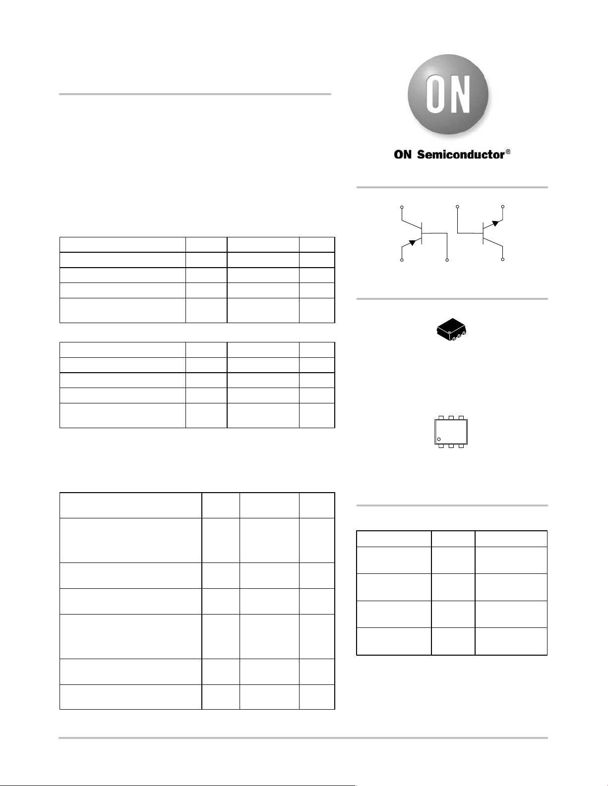
BC847BPDXV6T1,
BC847BPDXV6T5
Dual General Purpose
Transistor
NPN/PNP Dual (Complementary)
This transistor is designed for general purpose amplifier
applications. It is housed in the SOT−563 which is designed for low
power surface mount applications.
• Lead−Free Solder Plating
MAXIMUM RATINGS − NPN
Rating Symbol Value Unit
Collector−Emitter Voltage V
Collector−Base Voltage V
Emitter−Base Voltage V
Collector Current −
Continuous
CEO
CBO
EBO
I
C
MAXIMUM RATINGS − PNP
Rating Symbol Value Unit
Collector−Emitter Voltage V
Collector−Base Voltage V
Emitter−Base Voltage V
Collector Current −
Continuous
Maximum ratings are those values beyond which device damage can occur.
Maximum ratings applied to the device are individual stress limit values (not
normal operating conditions) and are not valid simultaneously . If these limits are
exceeded, device functional operation is not implied, damage may occur and
reliability may be affected.
CEO
CBO
EBO
I
C
THERMAL CHARACTERISTICS
Characteristic
(One Junction Heated)
Total Device Dissipation TA = 25°C
Derate above 25°C
Thermal Resistance −
Junction-to-Ambient
Characteristic
(Both Junctions Heated)
Total Device Dissipation
T
= 25°C
A
Derate above 25°C
Thermal Resistance −
Junction-to-Ambient
Junction and Storage
Temperature Range
1. FR−4 @ Minimum Pad
Symbol Max Unit
P
D
R
q
JA
Symbol Max Unit
P
D
R
q
JA
TJ, T
stg
45 V
50 V
6.0 V
100 mAdc
−45 V
−50 V
−5.0 V
−100 mAdc
357
(Note 1)
2.9
(Note 1)
350
(Note 1)
500
(Note 1)
4.0
(Note 1)
250
(Note 1)
−55 to +150 °C
mW
mW/°C
°C/W
mW
mW/°C
°C/W
http://onsemi.com
(3)
Q
1
(4) (5) (6)
BC847BPDX6T1
4
5
6
2
1
SOT−563
CASE 463A
PLASTIC
(1)(2)
Q
2
3
MARKING DIAGRAM
4F MG
G
1
4F = Specific Device Code
M = Month Code
G = Pb−Free Package
(Note: Microdot may be in either location)
ORDERING INFORMATION
Device Package Shipping
BC847BPDXV6T1 SOT−563 4 mm pitch
BC847BPDXV6T1G SOT−563
(Pb−Free)
BC847BPDXV6T5 SOT−563 4 mm pitch
BC847BPDXV6T5G SOT−563
(Pb−Free)
†For information on tape and reel specifications,
including part orientation and tape sizes, please
refer to our Tape and Reel Packaging Specification
Brochure, BRD8011/D.
4000/Tape & Reel
2 mm pitch
4000/Tape & Reel
8000/Tape & Reel
2 mm pitch
8000/Tape & Reel
†
© Semiconductor Components Industries, LLC, 2005
September, 2005 − Rev. 1
1 Publication Order Number:
BC847BPDXV6T1/D
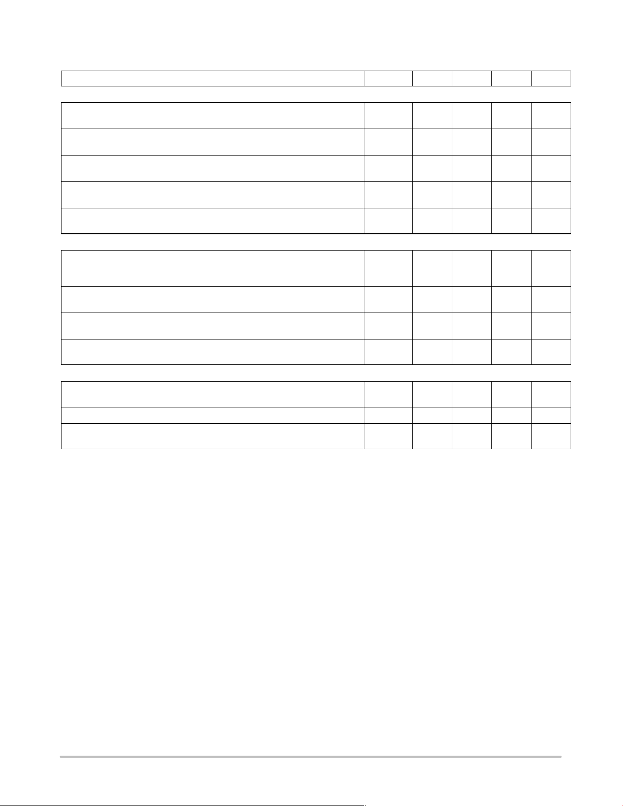
BC847BPDXV6T1, BC847BPDXV6T5
ELECTRICAL CHARACTERISTICS (NPN) (T
= 25°C unless otherwise noted)
A
Characteristic
OFF CHARACTERISTICS
Collector−Emitter Breakdown Voltage
(I
= 10 mA)
C
Collector−Emitter Breakdown Voltage
(I
= 10 μA, VEB = 0)
C
Collector−Base Breakdown Voltage
(I
= 10 mA)
C
Emitter−Base Breakdown Voltage
(I
= 1.0 mA)
E
Collector Cutoff Current (VCB = 30 V)
(V
= 30 V, TA = 150°C)
CB
ON CHARACTERISTICS
DC Current Gain
(I
= 10 μA, VCE = 5.0 V)
C
= 2.0 mA, VCE = 5.0 V)
(I
C
Collector−Emitter Saturation Voltage (IC = 10 mA, IB = 0.5 mA)
Collector−Emitter Saturation Voltage (I
= 100 mA, IB = 5.0 mA)
C
Base−Emitter Saturation Voltage (IC = 10 mA, IB = 0.5 mA)
Base−Emitter Saturation Voltage (I
= 100 mA, IB = 5.0 mA)
C
Base−Emitter Voltage (IC = 2.0 mA, VCE = 5.0 V)
Base−Emitter Voltage (I
= 10 mA, VCE = 5.0 V)
C
SMALL− SIGNAL CHARACTERISTICS
Current−Gain − Bandwidth Product
(I
= 10 mA, VCE = 5.0 Vdc, f = 100 MHz)
C
Output Capacitance (VCB = 10 V, f = 1.0 MHz) C
Noise Figure
(I
= 0.2 mA, VCE = 5.0 Vdc, RS = 2.0 kΩ, f = 1.0 kHz, BW = 200 Hz)
C
Symbol Min Typ Max Unit
V
(BR)CEO
45 − −
V
(BR)CES
50 − −
V
(BR)CBO
50 − −
V
(BR)EBO
6.0 − −
I
V
CE(sat)
V
BE(sat)
V
BE(on)
CBO
h
FE
f
T
obo
NF
−
−
−
200
−
−
−
−
580
−
−
−
150
290
−
−
0.7
0.9
660
−
15
5.0
−
475
0.25
0.6
−
−
700
770
nA
μA
mV
100 − − MHz
− − 4.5 pF
dB
− − 10
V
V
V
V
−
V
V
http://onsemi.com
2
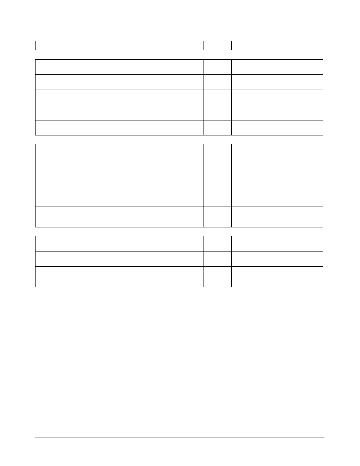
BC847BPDXV6T1, BC847BPDXV6T5
ELECTRICAL CHARACTERISTICS (PNP) (T
Characteristic
OFF CHARACTERISTICS
Collector−Emitter Breakdown Voltage
(I
= −10 mA)
C
Collector−Emitter Breakdown Voltage
(I
= −10 μA, VEB = 0)
C
Collector−Base Breakdown Voltage
(I
= −10 mA)
C
Emitter−Base Breakdown Voltage
(I
= −1.0 mA)
E
Collector Cutoff Current (VCB = −30 V)
Collector Cutoff Current (V
= −30 V, TA = 150°C)
CB
ON CHARACTERISTICS
DC Current Gain
(I
= −10 μA, VCE = −5.0 V)
C
= −2.0 mA, VCE = −5.0 V)
(I
C
Collector−Emitter Saturation Voltage
(I
= −10 mA, IB = −0.5 mA)
C
= −100 mA, IB = −5.0 mA)
(I
C
Base−Emitter Saturation Voltage
(I
= −10 mA, IB = −0.5 mA)
C
= −100 mA, IB = −5.0 mA)
(I
C
Base−Emitter On Voltage
(I
= −2.0 mA, VCE = −5.0 V)
C
= −10 mA, VCE = −5.0 V)
(I
C
SMALL− SIGNAL CHARACTERISTICS
Current−Gain − Bandwidth Product
(I
= −10 mA, VCE = −5.0 Vdc, f = 100 MHz)
C
Output Capacitance
(V
= −10 V, f = 1.0 MHz)
CB
Noise Figure
(I
= −0.2 mA, VCE = −5.0 Vdc, RS = 2.0 kΩ,
C
f = 1.0 kHz, BW = 200 Hz)
= 25°C unless otherwise noted)
A
Symbol Min Typ Max Unit
V
(BR)CEO
−45 − −
V
(BR)CES
−50 − −
V
(BR)CBO
−50 − −
V
(BR)EBO
−5.0 − −
I
CBO
h
V
CE(sat)
V
BE(sat)
V
BE(on)
C
FE
f
T
ob
−
−
−
200
−
−
−
−
−0.6
−
−
−
150
290
−
−
−0.7
−0.9
−
−
−15
−4.0
−
475
−0.3
−0.65
−
−
−0.75
−0.82
nA
μA
100 − − MHz
− − 4.5 pF
NF − − 10 dB
V
V
V
V
−
V
V
V
http://onsemi.com
3

BC847BPDXV6T1, BC847BPDXV6T5
TYPICAL NPN CHARACTERISTICS
2.0
1.5
1.0
0.8
0.6
0.4
, NORMALIZED DC CURRENT GAIN
0.3
FE
h
0.2
0.2 0.5 1.0 10 20
2.0 5.0
IC, COLLECTOR CURRENT (mAdc)
Figure 1. Normalized DC Current Gain
2.0
1.6
1.2
IC =
10 mA
0.8
IC = 50 mA IC = 100 mA
IC =
20 mA
TA = 25°C
IC = 200 mA
VCE = 10 V
T
= 25°C
A
50
100
200
V, VOLTAGE (VOLTS)
1.0
TA = 25°C
0.9
0.8
0.7
0.6
0.5
0.4
0.3
0.2
0.1
0
0.2 0.5 1.0 10 20
V
@ IC/IB = 10
BE(sat)
V
@ VCE = 10 V
BE(on)
V
@ IC/IB = 10
CE(sat)
2.0
IC, COLLECTOR CURRENT (mAdc)
Figure 2. “Saturation” and “On” Voltages
1.0
−55°C to +125°C
1.2
1.6
2.0
2.4
50
307.05.03.00.70.30.1
10070
0.4
, COLLECTOR−EMITTER VOLTAGE (V)
CE
V
0.02 1.0
0.1
IB, BASE CURRENT (mA)
Figure 3. Collector Saturation Region
10
7.0
5.0
3.0
2.0
C, CAPACITANCE (pF)
1.0
0.4 0.6 1.0 10 20
0.8 4.0 8.0
C
ib
C
ob
2.0 6.0
VR, REVERSE VOLTAGE (VOLTS)
Figure 5. Capacitances
TA = 25°C
10020
2.8
, TEMPERATURE COEFFICIENT (mV/ C)°θ
VB
0.2 1.0
IC, COLLECTOR CURRENT (mA)
10 100
Figure 4. Base−Emitter Temperature Coefficient
400
300
200
100
80
60
40
30
20
T
f, CURRENT−GAIN − BANDWIDTH PRODUCT (MHz)
40
0.7 1.0 10 202.0
IC, COLLECTOR CURRENT (mAdc)
VCE = 10 V
T
= 25°C
A
307.05.03.00.5
50
Figure 6. Current−Gain − Bandwidth Product
http://onsemi.com
4
BC847BPDXV6T1, BC847BPDXV6T5
TYPICAL PNP CHARACTERISTICS
2.0
1.5
1.0
0.7
0.5
, NORMALIZED DC CURRENT GAIN
0.3
FE
h
0.2
−2.0
−1.6
−1.2
−0.8
−0.4
, COLLECTOR−EMITTER VOLTAGE (V)
CE
V
VCE = −10 V
T
= 25°C
A
−0.2
−0.5 −1.0 −2.0 −5.0 −10 −20 −50 −100 −200 −0.1
IC, COLLECTOR CURRENT (mAdc)
Figure 7. Normalized DC Current Gain
TA = 25°C
−10 mA
IC = −20 mA
−0.02 −1.0
−0.1
IB, BASE CURRENT (mA)
IC = −200 mAIC = −50 mAIC =
IC = −100 mA
−100−20
V, VOLTAGE (VOLTS)
, TEMPERATURE COEFFICIENT (mV/ C)°θ
VB
−1.0
−0.9
−0.8
−0.7
−0.6
−0.5
−0.4
−0.3
−0.2
−0.1
1.0
1.2
1.6
2.0
2.4
2.8
TA = 25°C
V
@ IC/IB = 10
BE(sat)
V
@ VCE = −10 V
BE(on)
V
@ IC/IB = 10
CE(sat)
0
−0.2 −0.5
−1.0
−2.0 −5.0
IC, COLLECTOR CURRENT (mAdc)
−10
Figure 8. “Saturation” and “On” Voltages
−55°C to +125°C
−0.2
−1.0
IC, COLLECTOR CURRENT (mA)
−10 −100
−20 −50
−100
10
7.0
5.0
3.0
2.0
C, CAPACITANCE (pF)
1.0
−0.4
Figure 9. Collector Saturation Region
C
ib
TA = 25°C
C
ob
−0.6 −1.0 −2.0 −4.0 −6.0 −10 −20 −30 −40
VR, REVERSE VOLTAGE (VOLTS)
Figure 11. Capacitances
http://onsemi.com
Figure 10. Base−Emitter Temperature
Coefficient
400
300
200
150
100
80
60
40
30
20
T
f, CURRENT−GAIN − BANDWIDTH PRODUCT (MHz)
−0.5
−1.0 −2.0 −3.0 −5.0 −10 −20 −30 −50
IC, COLLECTOR CURRENT (mAdc)
VCE = −10 V
T
= 25°C
A
Figure 12. Current−Gain − Bandwidth Product
5

BC847BPDXV6T1, BC847BPDXV6T5
INFORMATION FOR USING THE SOT−563 SURFACE MOUNT PACKAGE
e
n
e
s
g
-
n
s
e
.
-
e
MINIMUM RECOMMENDED FOOTPRINT FOR SURFACE MOUNTED APPLICATIONS
Surface mount board layout is a critical portion of the
total design. The footprint for the semiconductor packages
must be the correct size to insure proper solder connection
1.35
interface between the board and the package. With th
correct pad geometry, the packages will self align whe
subjected to a solder reflow process.
0.3
0.45
1.0
0.50.5
Dimensions in mm
SOT−563
SOT−563 POWER DISSIPATION
The power dissipation of the SOT−563 is a function of
the pad size. This can vary from the minimum pad size for
soldering to a pad size given for maximum power dissipation. Power dissipation for a surface mount device is determined by T
of the die, R
junction to ambient, and the operating temperature, T
, the maximum rated junction temperature
J(max)
, the thermal resistance from the device
JA
θ
A
Using the values provided on the data sheet for the
SOT−563 package, P
can be calculated as follows:
D
T
− T
PD =
J(max)
R
A
θ
JA
The values for the equation are found in the maximum
ratings table on the data sheet. Substituting these values
into the equation for an ambient temperature T
of 25°C,
A
one can calculate the power dissipation of the device which
in this case is 150 milliwatts.
The melting temperature of solder is higher than th
rated temperature of the device. When the entire device i
heated to a high temperature, failure to complete solderin
within a short time could result in device failure. There
fore, the following items should always be observed i
order to minimize the thermal stress to which the device
.
are subjected.
• Always preheat the device.
• The delta temperature between the preheat and
soldering should be 100°C or less.*
• When preheating and soldering, the temperature of th
leads and the case must not exceed the maximum
temperature ratings as shown on the data sheet. When
using infrared heating with the reflow soldering
method, the difference shall be a maximum of 10°C.
SOLDERING PRECAUTIONS
• The soldering temperature and time shall not exceed
150°C − 25°C
PD =
833°C/W
= 150 milliwatts
The 833°C/W for the SOT−563 package assumes the use
of the recommended footprint on a glass epoxy printed
circuit board to achieve a power dissipation of 150 milliwatts. There are other alternatives to achieving higher
power dissipation from the SOT−563 package. Another
alternative would be to use a ceramic substrate or an
aluminum core board such as Thermal Clad
®
. Using a
board material such as Thermal Clad, an aluminum core
board, the power dissipation can be doubled using the same
footprint.
260°C for more than 10 seconds.
• When shifting from preheating to soldering, the
maximum temperature gradient shall be 5°C or less.
• After soldering has been completed, the device should
be allowed to cool naturally for at least three minutes
Gradual cooling should be used as the use of forced
cooling will increase the temperature gradient and
result in latent failure due to mechanical stress.
• Mechanical stress or shock should not be applied
during cooling.
* Soldering a device without preheating can cause exces
sive thermal shock and stress which can result in damag
http://onsemi.com
6

D
−X−
6
12 3
e
45
b
0.08 (0.003) X
E
−Y−
6 5 PL
BC847BPDXV6T1, BC847BPDXV6T5
PACKAGE DIMENSIONS
SOT−563, 6 LEAD
CASE 463A−01
ISSUE F
NOTES:
1. DIMENSIONING AND TOLERANCING PER ANSI
Y14.5M, 1982.
A
L
H
E
C
M
Y
SOLDERING FOOTPRINT*
0.3
0.0118
2. CONTROLLING DIMENSION: MILLIMETERS
3. MAXIMUM LEAD THICKNESS INCLUDES LEAD
FINISH THICKNESS. MINIMUM LEAD THICKNESS
IS THE MINIMUM THICKNESS OF BASE MATERIAL.
DIM MIN NOM MAX
A 0.50 0.55 0.60
b 0.17 0.22 0.27
C
0.08 0.12 0.18 0.003 0.005 0.007
D 1.50 1.60 1.70
E 1.10 1.20 1.30
e 0.5 BSC
L 0.10 0.20 0.30
H
1.50 1.60 1.70
E
MILLIMETERS
INCHES
MIN NOM MAX
0.020 0.021 0.023
0.007 0.009 0.011
0.059 0.062 0.066
0.043 0.047 0.051
0.02 BSC
0.004 0.008 0.012
0.059 0.062 0.066
0.45
0.0177
1.0
1.35
0.0394
0.0531
0.5
0.5
0.0197
0.0197
mm
ǒ
SCALE 20:1
inches
Ǔ
*For additional information on our Pb−Free strategy and soldering
details, please download the ON Semiconductor Soldering and
Mounting Techniques Reference Manual, SOLDERRM/D.
http://onsemi.com
7

BC847BPDXV6T1, BC847BPDXV6T5
ON Semiconductor and are registered trademarks of Semiconductor Components Industries, LLC (SCILLC). SCILLC reserves the right to make changes without further notice
to any products herein. SCILLC makes no warranty, representation or guarantee regarding the suitability of its products for any particular purpose, nor does SCILLC assume any liability
arising out of the application or use of any product or circuit, and specifically disclaims any and all liability, including without limitation special, consequential or incidental damages.
“Typical” parameters which may be provided in SCILLC data sheets and/or specifications can and do vary in different applications and actual performance may vary over time. All
operating parameters, including “Typicals” must be validated for each customer application by customer’s technical experts. SCILLC does not convey any license under its patent rights
nor the rights of others. SCILLC products are not designed, intended, or authorized for use as components in systems intended for surgical implant into the body, or other applications
intended to support or sustain life, or for any other application in which the failure of the SCILLC product could create a situation where personal injury or death may occur. Should
Buyer purchase or use SCILLC products for any such unintended or unauthorized application, Buyer shall indemnify and hold SCILLC and its officers, employees, subsidiaries, affiliates,
and distributors harmless against all claims, costs, damages, and expenses, and reasonable attorney fees arising out of, directly or indirectly, any claim of personal injury or death
associated with such unintended or unauthorized use, even if such claim alleges that SCILLC was negligent regarding the design or manufacture of the part. SCILLC is an Equal
Opportunity/Affirmative Action Employer. This literature is subject to all applicable copyright laws and is not for resale in any manner.
PUBLICATION ORDERING INFORMATION
LITERATURE FULFILLMENT:
Literature Distribution Center for ON Semiconductor
P.O. Box 61312, Phoenix, Arizona 85082−1312 USA
Phone: 480−829−7710 or 800−344−3860 Toll Free USA/Canada
Fax: 480−829−7709 or 800−344−3867 Toll Free USA/Canada
Email: orderlit@onsemi.com
N. American Technical Support: 800−282−9855 Toll Free
USA/Canada
Japan: ON Semiconductor, Japan Customer Focus Center
2−9−1 Kamimeguro, Meguro−ku, Tokyo, Japan 153−0051
Phone: 81−3−5773−3850
http://onsemi.com
ON Semiconductor Website: http://onsemi.com
Order Literature: http://www.onsemi.com/litorder
For additional information, please contact your
local Sales Representative.
BC847CBPDXV6T1/D
8
 Loading...