

Page 1
AR0330CS
AR0330CS and AR0330SR
1/3-Inch CMOS Digital
Image Sensor
General Description
The AR0330CS can be operated in its default mode or programmed
for frame size, exposure, gain, and other parameters. The default mode
output is a 2304 x 1296 image at 30 frames per second (fps). The
sensor outputs 10− or 12−bit raw data, using either the parallel or serial
(MIPI) output ports.
The ON Semiconductor AR0330CS is a 1/3−inch CMOS digital
image sensor with an active−pixel array of 2304 (H) x1536 (V). It can
support 3.15 megapixel (2048H x 1536 V) digital still image capture
and a 1080p30 +20%EIS (2304H x 1296 V) digital video mode. It
incorporates sophisticated on−chip camera functions such as
windowing, mirroring, column and row subsampling modes, and
snapshot modes.
Table 1. KEY PARAMETERS
Parameter Typical Value
Optical Format 1/3−inch (6.0 mm)
Entire Array: 6.09 mm
Still Image: 5.63 mm (4:3)
HD Image: 5.82 mm (16:9)
Active Pixels 2304(H) x 1536(V): (Entire Array):
5.07 mm (H) x 3.38 mm (V)
2048(H) x 1536(V) (4:3, Still Mode)
2304(H) x 1296(V) (16:9, sHD Mode)
Pixel Size
Color Filter Array RGB Bayer
Shutter Type ERS and GRR
Input Clock Range 6 – 27 MHz
Output Clock Maximum
(CLK_OP)
Responsivity 2.0 V/lux−sec
Power Consumption
SNR
MAX
Dynamic Range 69.5 dB
Supply
Voltage
Operating Temperature
(junction) −T
Package Options 6.28 mm x 6.65 mm CSP
I/O/Digital 1.7–1.9 V (1.8 V Nominal) or
Digital 1.7–1.9 V (1.8 V Nominal)
Analog 2.76–2.9 V
J
2.2 mm x 2.2 mm
98 Mp/s (Parallel, MIPI)
1080P30 MIPI Mode: 282 mW
1080P30 Parallel Mode: 252 mW
39 dB
2.4–3.1 V (2.8 V Nominal)
–30°C to + 70° C
11.43 mm x 11.43 mm PLCC
www.onsemi.com
PLCC48
11.43x11.43
CASE 776AM
ORDERING INFORMATION
See detailed ordering and shipping information on page 2 of
this data sheet.
Features (continued)
ODCSP64
6.278x6.648
CASE 570BH
• 2.2 mm Pixel with ON Semiconductor
A−Pix
™ technology
• Superior Low−light Performance
• 3.5 Mp Active Array, 2.9 Mp (16:9) Video
3.4 Mp (3:2) and 3.15 Mp (4:3) Still Images
• Support for External Mechanical Shutter
• Support for External LED or Xenon Flash
• Data Interfaces: Two−lane Serial MIPI or
Parallel Interface
• On−chip phase−locked Loop (PLL)
Oscillator
• Integrated Position−based Color and Lens
Shading Correction
• Simple Two−wire Serial Interface
• Auto Black Level Calibration
• 12−to−10 bit Output A−Law Compression
• Slave Mode for Precise Frame−rate Control
and for Synchronizing Two Sensors
Applications
• 1080P30 High−definition Digital Video
Camcorder
• Web Cameras and Video Conferencing
Cameras
• Security
© Semiconductor Components Industries, LLC, 2012
January, 2019 − Rev. 8
1 Publication Order Number:
AR0330CS/D
Page 2
AR0330CS
ORDERING INFORMATION
Table 2. AVAILABLE PART NUMBERS
Part Number
AR0330CS1C12SPKA0−CP 3.5 MP, 1/3−inch, 12 Deg CRA, Parallel, MIPI, CSP Tray, Protective Film
AR0330CS1C12SPKA0−CR 3.5 MP, 1/3−inch, 12 Deg CRA, Parallel, MIPI, CSP Tray, No Protective Film
AR0330CSSC12SPBA0−DR 3.5 MP, 1/3−inch, 12 Deg CRA, Parallel, PLCC Tray, No Protective Film
AR0330SR1C00SUKA0−CP 3.5 MP, 1/3−inch, 0 Deg CRA, Parallel, CSP Tray, Protective Film
AR0330SR1C00SUKA0−CR 3.5 MP, 1/3−inch, 0 Deg CRA, Parallel, CSP Tray, No Protective Film
AR0330CS1C12SPKAH3−GEVB 3.5 MP, 1/3− inch, 12 Deg CRA, Parallel, MIPI, CSP Evaluation board
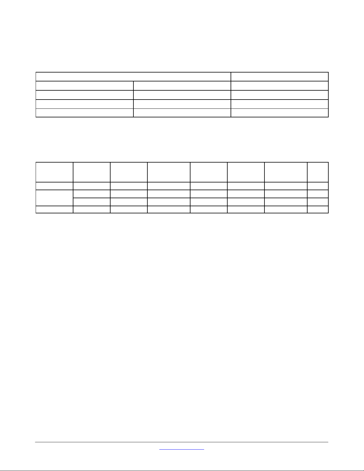
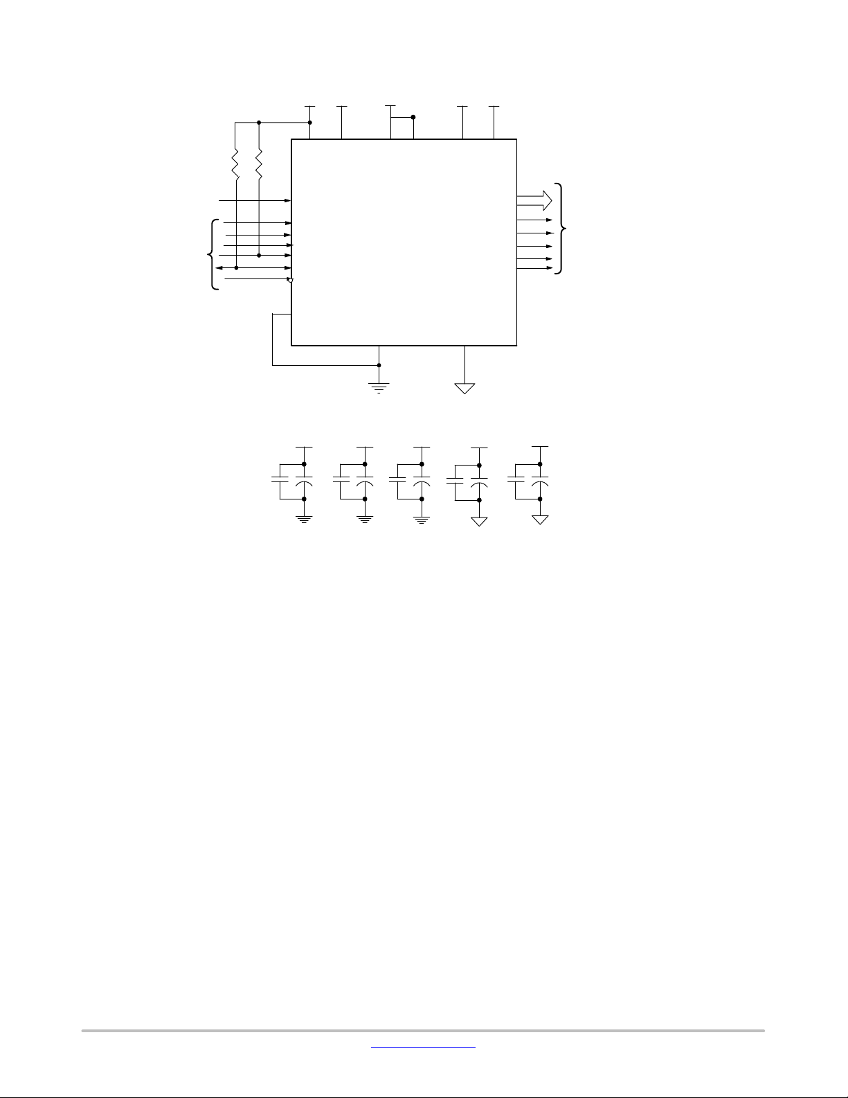
FUNCTIONAL OVERVIEW
The AR0330CS is a progressive−scan sensor that
generates a stream of pixel data at a constant frame rate. It
uses an on−chip, phase−locked loop (PLL) that can generate
all internal clocks from a single master input clock running
Ext
Clock
Analog Core
PLL
Timing
and
Control
Registers
Pixel Array
Row Drivers
Column
Amplifiers
ADC
12−bit
Product Description Orderable Product Attribute Description
between 6 and 27 MHz. The maximum CLK_OP is 98 Mp/s
using MIPI serial interface and 98 Mp/s using the parallel
interface.
Test Pattern
Generator
Digital Core
Row Noise Correction
Black Level Correction
Lens Shading Correction
Digital Gain
Data Pedestal
12−bit
12−bit
Output Data−Path
Compression (optional)
12−bit
8, 10, or
12−bit
Two−wire serial I/F
Figure 1. Block Diagram
User interaction with the sensor is through the two−wire
serial bus, which communicates with the array control,
analog signal chain, and digital signal chain. The core of the
sensor is a 3.5 Mp active− pixel sensor array. The timing and
control circuitry sequences through the rows of the array,
resetting and then reading each row in turn. In the time
interval between resetting a row and reading that row, the
pixels in the row integrate incident light. The exposure is
Parallel I/O:
PIXCLK, FV,
LV, D
OUT [11:0]
Ma x 98 Mp/s
MIPI I/O:
CLK P/N,
1. Two lane data paths
only 2. 98 Mp/sec
Max CLK_OP 98 Mp/s
controlled by varying the time interval between reset and
readout. Once a row has been read, the signal from the
column is amplified in a column amplifier and then digitized
in an analog−to−digital converter (ADC). The output from
the ADC is a 12−bit value for each pixel in the array. The
ADC output passes through a digital processing signal chain
(which provides further data path corrections and applies
digital gain).
www.onsemi.com
2
Page 3
AR0330CS
WORKING MODES
The AR0330CS sensor working modes are specified from
the following aspect ratios:
Table 3. AVAILABLE ASPECT RATIOS IN THE AR0330CS SENSOR
Aspect Ratio Sensor Array Usage
3:2 Still Format #1 2256(H) x 1504(V)
4:3 Still Format #2 2048 (H) x 1536 (V)
16:10 Still Format #3 2256 (H) x 1440 (V)
16:9 FHD Format 2304 (H) x 1296 (V)
The AR0330CS supports the following working modes.
To operate the sensor at full speed 98Mp/s the sensor must
operate at full−speed (98 Mp/s) when using the parallel
interface.
use 2−Lane MIPI or parallel interface. The sensor will
Table 4. AVAILABLE WORKING MODES IN THE AR0330CS SENSOR
Active
Readout
Mode Aspect Ratio
1080p + EIS 16:9 2304 x 1296 2304 x 1296 30 30 – 100%
3M Still
WVGA + EIS 16:9 2304 x 1296 1152 x 648 60 60 2 x 2 100%
4:3 2048 x 1536 2048 x 1536 30 25 – 100%
3:2 2256 x 1504 2256 x 1504 30 25 – 100%
Window
Sensor Output
Resolution
FPS
(2 lane MIPI,
12 bit)
FPS (Parallel
Interface)
Subsampling FOV
www.onsemi.com
3
Page 4
Digital
I/O
power
1
AR0330CS
Digital
Core
1
power
PLL
power
1
Analog
power
1
Analog
1
power
Master clock
(6–27MHz)
From
controller
3, 4
1.5kΩ
3, 4
VDD_IO
1.5kΩ
EXTCLK
TRIGGER
SADDR
SCLK
SDATA
RESET_BAR
TEST
VDD_IO VDD_PLLVDD
0.1 μF10 μF
VDD
VAA VAA_PIX
DATA1_P
V DD_MIPI
VDD_PLL
DATA1_N
DATA2_P
DATA2_N
CLK_P
CLK_N
To
controller
(MIPI − serial interface)
SHUTTER
FLASH
GND AGND
D
Digital
ground
0.1 μF10 μF
10 μF
0.1 μF
Analog
ground
VAA
0.1 μF10 μF
10 μF
VAA_PIX
0.1 μF
1. All power supplies must be adequately decoupled. ON Semiconductor recommends having 10 mF and 0.1 mF decoupling capacitors for
every power supply. If space is a concern, then priority must be given in the following order: V
DD. Actual values and results may vary depending on layout and design considerations.
and V
AA, VAA_PIX, VDD_PLL, VDD_MIPI, VDD_IO,
2. To allow for space constraints, ON Semiconductor recommends having 0.1 mF decoupling capacitor inside the module as close to the
pads as possible. In addition, place a 10 mF capacitor for each supply off−module but close to each supply.
3. ON Semiconductor recommends a resistor value of 1.5 kW, but a greater value may be used for slower two−wire speed.
4. The pull−up resistor is not required if the controller drives a valid logic level on S
CLK at all times.
5. ON Semiconductor recommends that analog power planes are placed in a manner such that coupling with the digital power planes is
minimized.
6. TEST pin must be tied to D
7. ON Semiconductor recommends that GND_MIPI be tied to D
DD_MIPI is tied to VDD_PLL in the CSP package. ON Semiconductor strongly recommends that VDD_MIPI must be connected to a
8. V
DD_PLL in a module design since VDD_PLL and VDD_MIPI are tied together in the die.
V
GND for the MIPI configuration.
GND.
9. The package pins or die pads used for the parallel interface must be left floating.
10.If the SHUTTER or FLASH pins or pads are not used, then they must be left floating.
11.If the TRIGGER or OE_BAR pin or pad is not used, then it should be tied to D
GND.
Figure 2. Typical Configuration: Serial MIPI
www.onsemi.com
4
Page 5
Master clock
(6–27 MHz)
From
Controller
3, 4
AR0330CS
Digital
Digital
core
I/O
1
power
power
VDD_IO
3, 4
1.5k
1.5k
VDD
EXTCLK
OE_BAR
TRIGGER
SADDR
SCLK
SDATA
RESET_BAR
TEST
PLL
GND
D
power
1
V DD_PLL
1
VDD_MIPI
Analog
Analog
1
power
power
VAA_PIX
VAA
DOUT [11:0]
PIXCLK
LINE_VALID
FRAME_VALID
FLASH
SHUTTER
AGND
1
To
controller
10 μF
DD_IO VDD_PLLVDD
V
0.1 μF
10 μF
Digital
ground
10 μF
0.1 μF
10 μF
Analog
ground
0.1 μF
VAA
VAA_PIX
10 μF0.1 μF
0.1 μF
12.All power supplies must be adequately decoupled. ON Semiconductor recommends having 10 mF and 0.1 mF decoupling capacitors for
every power supply. If space is a concern, then priority must be given in the following order: V
AA, VAA_PIX, VDD_PLL, VDD_IO, and VDD.
Actual values and results may vary depending on layout and design considerations.
13.To allow for space constraints, ON Semiconductor recommends having 0.1 mF decoupling capacitor inside the module as close to the
pads as possible. In addition, place a 10 mF capacitor for each supply off−module but close to each supply.
14.ON Semiconductor recommends a resistor value of 1.5 kW, but a greater value may be used for slower two−wire speed.
15.The pull−up resistor is not required if the controller drives a valid logic level on S
CLK at all times.
16.ON Semiconductor recommends that analog power planes are placed in a manner such that coupling with the digital power planes is
minimized.
17.TEST pin should be tied to the ground.
18.The data and clock package pins or die pads used for the MIPI interface must be left floating.
19.The V
DD_MIPI package pin and sensor die pad should be connected to a 2.8 V supply as it is tied to the VDD_PLL supply both in the
package routing and also within the sensor die itself.
20.If the SHUTTER or FLASH pins or pads are not used, then they must be left floating.
21.If the TRIGGER or OE_BAR pin or pad is not used, then it should be tied to D
GND.
Figure 3. Typical Configuration: Parallel Pixel Data Interface
www.onsemi.com
5
Page 6

AR0330CS
PIN DESCRIPTIONS
Table 5. PIN DESCRIPTIONS
Name Type Description
RESET_BAR Input Asynchronous reset (active LOW). All settings are restored to factory default
EXTCLK Input Master input clock, range 6 − 27 MHz
TRIGGER Input Receives slave mode VD signal for frame rate synchronization and trigger to start a GRR frame
SADDR Input Two−wire serial address select
SCLK Input Two−wire serial clock input
TEST Input Enable manufacturing test modes. Tie to DGND for normal sensor operation
OE_BAR Input Parallel port output enable, active low
SDATA I/O Two−wire serial data I/O
PIXCLK Output Pixel clock out. DOUT is valid on rising edge of this clock
DOUT[11:0] Output Parallel pixel data output
FLASH Output Flash output. Synchronization pulse for external light source. Can be left floating if not used
FRAME_VALID Output Asserted when DOUT data is valid
LINE_VALID Output LINE_VALID output asserted when DOUT data is valid
SHUTTER Output Control for external mechanical shutter. Can be left floating if not used
DATA1_P Output MIPI serial data, lane 1, differential P
DATA1_N Output MIPI serial data, lane 1, differential N
DATA2_P Output MIPI serial data, lane 2, differential P
DATA2_N Output MIPI serial data, lane 2, differential N
CLK_P Output Output MIPI serial clock, differential P
CLK_N Output Output MIPI serial clock, differential N
VDD_MIPI Power MIPI power supply
VAAHV_NPIX Power Power supply pin used to program the sensor OTPM (one−time programmable memory). This pin
VDD Power Digital power
VDD_IO Power IO supply power
VDD_PLL Power PLL power supply
DGND Power Digital GND
VAA Power Analog power
VAA_PIX Power Pixel power
AGND Power Analog GND
should be open if OTPM is not used
www.onsemi.com
6
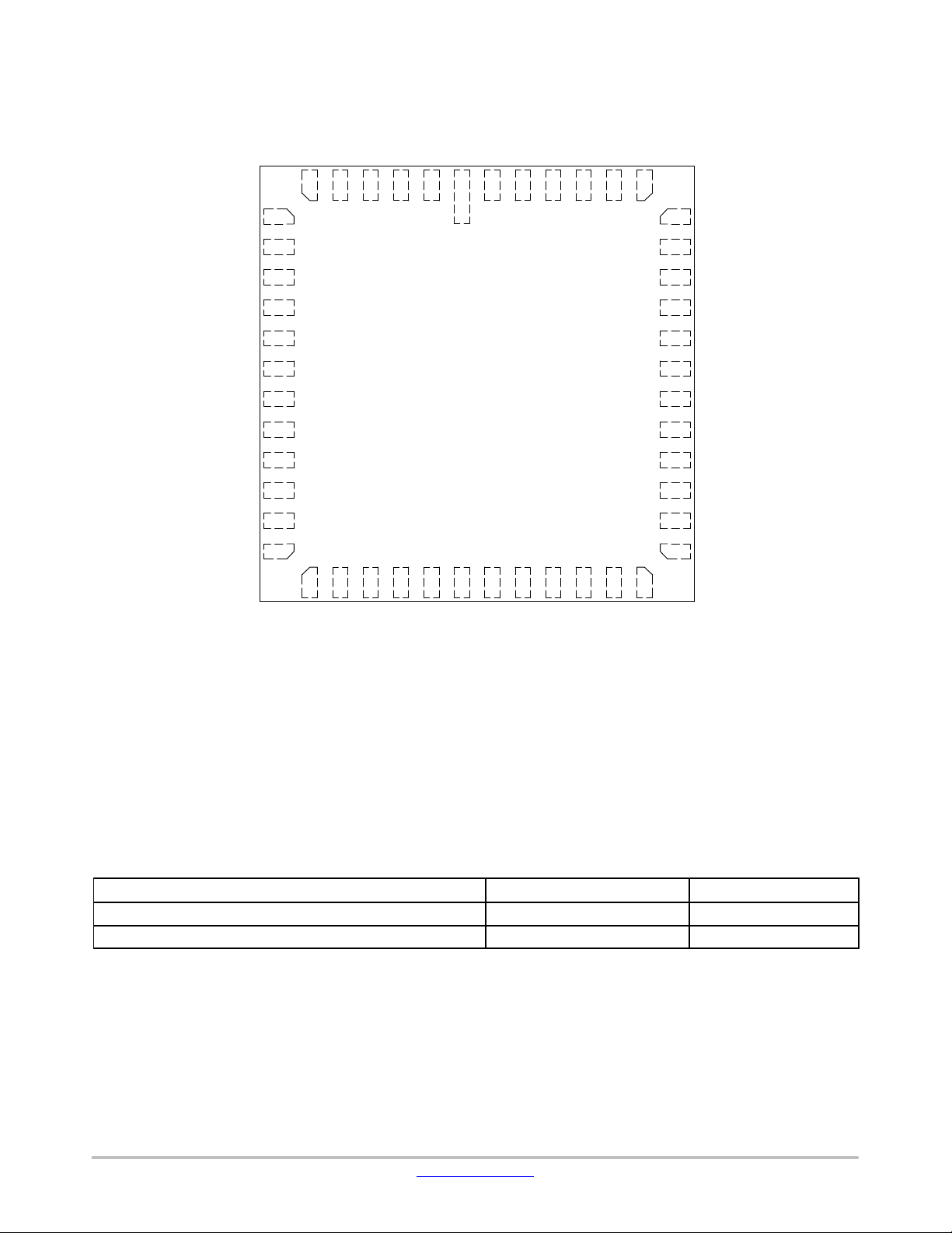
Page 7
AR0330CS
Table 6. AR0330CS CSP (PARALLEL/MIPI) PACKAGE PINOUT
1 2 3 4 5 6 7 8
A
B
C
D
E
F
G
H
22.NC = Do not connect. For manufacturing test purpose only.
VAA VAAHV_NPIX AGND NC VAA_PIX VAA VDD_IO VDD
VDD SDATA FRAME_VALID DGND AGND DGND TEST SHUTTER
SADDR FLASH LINE_VALID DGND DGND DGND TRIGGER RESET_BAR
SCLK VDD_IO DOUT10 DGND VDD_IO VDD_IO EXTCLK DATA_N
PIXCLK DOUT11 DOUT9 DOUT7 VDD_IO DGND CLK_N DATA_P
– – DOUT8 DOUT6 DOUT4 VDD_IO CLK_P VDD_PLL
DGND VDD DOUT5 DOUT3 DOUT1 DOUT0 DATA2_N VDD
– DGND DGND DOUT2 VDD_IO VDD_MIPI DATA2_P VDD_MIPI
Table 7. AR0330SR CSP (PARALLEL) PACKAGE PINOUT
1 2 3 4 5 6 7 8
A
B
C
D
E
F
VAA VAAHV_NPIX AGND NC VAA_PIX VAA VDD_IO VDD
VDD SDATA FRAME_VALID DGND AGND DGND TEST SHUTTER
SADDR FLASH LINE_VALID DGND DGND DGND TRIGGER RESET_BAR
SCLK VDD_IO DOUT10 DGND VDD_IO VDD_IO EXTCLK –
PIXCLK DOUT11 DOUT9 DOUT7 VDD_IO DGND – –
– – DOUT8 DOUT6 DOUT4 VDD_IO – VDD_PLL
G
DGND VDD DOUT5 DOUT3 DOUT1 DOUT0 – VDD
H
23.NC = Do not connect. For manufacturing test purpose only.
– DGND DGND DOUT2 VDD_IO VDD_PLL – VDD_PLL
www.onsemi.com
7
Page 8
AR0330CS
GND
V
DD_IO 7
V
DD_IO 8
CLK 9
S
S
ADDR 10
EXTCLK 11
PIXCLK 12
FLASH 13
S
DATA 14
FRAME_VALID 15
LINE_VALID 16
OUT 11 17
D
DOUT10 18
6 DGND
5 DGND
4 VDD
3 VDD
2 D
1 V DD _PLL
48 AGND
47 AGND
46 VAA
45 VAA
44 VAA
43 AGND
42 AGND
41 VAA_PIX
AA_PIX
40 V
39 AGND
38 AGND
37 NC
AA HV_NPIX
36 V
35 NC
34 V
DD
33 TRIGGER
32 OE_BAR
31 TEST
OUT 9 19
D
D
D
D
OUT 4 24
D
D
OUT 5 23
OUT 6 22
OUT 7 21
OUT 8 20
TOP VIEW
Figure 4. PLCC Pinout
Table 8. AR0330CS PLCC PACKAGE THERMAL RESISTANCE
Junction to ambient air thermal resistance (qJA) (°C/W)
Junction to board thermal resistance (qJB) (°C/W)
OUT 3 25
D
D
D
D
NC 29
OUT 0 28
OUT 1 27
OUT 2 26
RESET_BAR 30
Using JEDEC 1S0P Board Using JEDEC 2S2P Board
51.47 36.92
22.16 21.73
www.onsemi.com
8
Page 9
AR0330CS
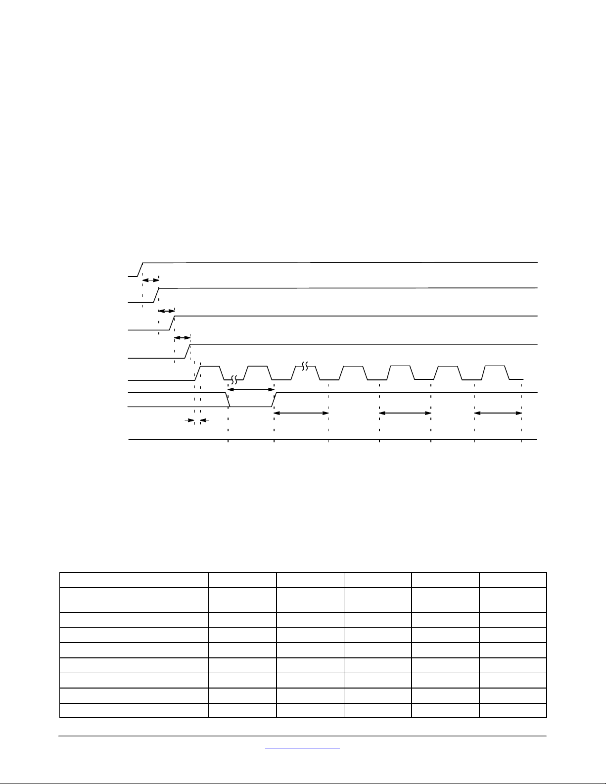
SENSOR INITIALIZATION
Power−Up Sequence
The recommended power−up sequence for the
AR0330CS is shown in Figure 5. The available power
supplies (V
must have the separation specified below.
DD
DD_IO, VDD_PLL, VDD_MIPI, VAA, VAA_PIX)
1. Turn on V
2. After 100 μs, turn on V
DD_PLL and VDD_MIPI power supplies
AA and VAA_PIX power
supply
3. After 100 μs, turn on V
4. After 100 μs, turn on V
DD power supply
DD_IO power supply
5. After the last power supply is stable, enable
EXTCLK
6. Assert RESET_BAR for at least 1ms
V
DD
_MIPI (2.8)
V
AA
(2.8)
AA
t
0
t
1
7. Wait 150,000 EXTCLKs (for internal initialization
into software standby
8. Write R0x3052 = 0xA114 to configure the internal
register initialization process
9. Write R0x304A = 0x0070 to start the internal
register initialization process
10. Wait 150,000 EXTCLK periods
11. Configure PLL, output, and image settings to
desired values
12. Wait 1 ms for the PLL to lock
13. Set streaming mode (R0x301A[2] = 1)
V
(1.8)
DD
V
_IO (1.8/2.8)
DD
EXTCLK
RESET_BAR
24.A software reset (R0x301A[0] = 1) is not necessary after the procedure described above since a Hard Reset will automatically triggers
a software reset. Independently executing a software reset, should be followed by steps seven through thirteen above
25.The sensor must be receiving the external input clock (EXTCLK) before the reset pin is toggled. The sensor will begin an internal
initialization sequence when the reset pin toggle from LOW to HIGH. This initialization sequence will run using the external input clock.
Power on default state is software standby state, need to apply two−wire serial commands to start streaming. Above power up sequence
is a general power up sequence. For different interface configurations, MIPI, and Parallel, some power rails are not needed. Those not
needed power rails should be ignored in the general power up sequence..
t
2
t
3
t
X
t
4
t
5
Software
Standby PLL Clock
t
6
Figure 5. Power Up
Table 9. POWER−UP SEQUENCE
Definition Symbol Min Ty p Max Unit
VDD_PLL, VDD_MIPI to VAA/VAA_PIX
(Note 28)
VAA/VAA_PIX to VDD t1 0 100 –
VDD to VDD_IO t2 0 100 –
External clock settling time tx – 30 (Note 26) – ms
Hard Reset t3 1 (Note 27) – – ms
Internal Initialization t4 150000 – – EXTCLKs
Internal Initialization t5 150000 – – EXTCLKs
PLL Lock Time t6 1 – – ms
t0 0 100 –
ms
ms
ms
Streaming
www.onsemi.com
9
Page 10
AR0330CS
26.External clock settling time is component−dependent, usually taking about 10 – 100 ms.
27.Hard reset time is the minimum time required after power rails are settled. In a circuit where Hard reset is held down by RC circuit, then the
RC time must include the all power rail settle time and Xtal settle time.
28.It is critical that V
others. If the case happens that V
current draw on this supply.
DD_MIPI is tied to VDD_PLL in the CSP package and must be powered to 2.8 V.
29.V
Power−Down Sequence
The recommended power−down sequence for the
AR0330CS is shown in Figure 6. The available power
supplies (V
must have the separation specified below.
1. Disable streaming if output is active by setting
standby R0x301a[2] = 0
VDD_HiSPi_TX (0.4)
V
_IO (1.8/2.8)
DD
DD
DD_PLL is not powered up after the other power supplies. It must be powered before or at least at the same time as the
DD_PLL is powered after other supplies then sensor may have functionality issues and will experience high
2. The soft standby state is reached after the current
row or frame, depending on configuration, has
DD_IO, VDD_PLL, VDD_MIPI., VAA, VAA_PIX)
ended
3. Turn off V
4. Turn off V
DD_IO
DD
5. Turn off VAA/VAA_PIX
V
_HiSPi (1.8)
DD
6. Turn off V
t
0
t
1
t
2
DD_PLL, VDD_MIPI
VAA_PIX, VAA (2.8)
t
3
V
DD
_MIPI (2.8)
DD
EXTCLK
t
4
Power Down until Next
Power Up Cycle
Figure 6. Power Down
Table 10. POWER−DOWN SEQUENCE
Definition Symbol Minimum Typical Maximum Unit
VDD_IO t0 0 – –
VDD_IO to VDD t1 0 – –
VDD to VAA/VAA_PIX t2 0 – –
VAA/VAA_PIX to VDD_PLL t3 0 – –
PwrDn until Next PwrUp Time t4 100 – – ms
30.t4 is required between power down and next power up time; all decoupling caps from regulators must be completely discharged.
ms
ms
ms
ms
www.onsemi.com
10
Page 11
STANDBY MODE
AR0330CS
Soft Standby
1. Disable streaming by setting standby R0x301a[2]
= 0
2. Delay 10 ms
3. Stop EXTCLK; pull EXTCLK pin LOW
Hard Standby
1. Disable streaming by setting standby R0x301a[2]
= 0
2. Delay 10 ms
3. Pull RESET_BAR to LOW
ELECTRICAL CHARACTERISTICS
Table 11. DC Electrical Definitions and Characteristics (MIPI Mode)
f
EXTCLK = 24 MHz; VDD = 1.8 V; VDD_IO = 1.8 V; VAA = 2.8 V; VAA_PIX = 2.8 V;
DD_PLL = 2.8 V; Output load = 68.5 pF; T
V
Definition
Core digital voltage VDD 1.7 1.8 1.9 V
I/O digital voltage VDD_IO
Analog voltage VAA 2.76 2.8 2.9 V
Pixel supply voltage VAA_PIX 2.76 2.8 2.9 V
PLL supply voltage VDD_PLL 2.7 2.8 2.9 V
MIPI supply voltage VDD_MIPI 2.7 2.8 2.9 V
Digital operating current − 114 − mA
I/O digital operating current − 0 − mA
Analog operating current − 41 − mA
Pixel supply current − 9.9 − mA
PLL supply current − 15 − mA
MIPI digital operating current − 35 − mA
= 60°C; Data Rate = 588 Mbps; DLL set to 0; 2304 x 1296 at 30 fps
J
Symbol Min Typ Max Unit
1.7 1.8 1.9 V
2.4 2.8 3.1 V
Table 12. DC Electrical Definitions and Characteristics (Parallel Mode)
f
= 24 MHz; VDD = 1.8 V; VDD_IO = 1.8 V; VAA = 2.8 V; VAA_PIX = 2.8 V;
EXTCLK
DD_PLL = 2.8 V; Output load = 68.5 pF; TJ = 60°C; 2304 x 1296 at 30 fps
V
Definition
Core digital voltage VDD 1.7 1.8 1.9 V
I/O digital voltage VDD_IO
Analog voltage VAA 2.76 2.8 2.9 V
Pixel supply voltage VAA_PIX 2.76 2.8 2.9 V
PLL supply voltage VDD_PLL 2.7 2.8 2.9 V
Digital operating current I(VDD) 66.5 75 mA
I/O digital operating current I(VDD_IO) 24 35 mA
Analog operating current I(VAA) 36 44 mA
Pixel supply current I(VAA_PIX) 10.5 18 mA
PLL supply current I(VDD_PLL) 6 11 mA
Symbol Min Typ Max Unit
1.7 1.8 1.9 V
2.4 2.8 3.1 V
www.onsemi.com
11
Page 12
AR0330CS
Table 13. STANDBY POWER
f
= 24 MHz; VDD = 1.8 V; VDD_IO = 1.8 V; VAA = 2.8 V; VAA_PIX = 2.8 V;
EXTCLK
DD_PLL = 2.8 V; Output load = 68.5 pF; TJ = 60°C
V
Power Typical Max Unit
Hard Standby (CLK OFF)
Soft Standby (CLK OFF)
Soft Standby (CLK ON)
Table 14. ABSOLUTE MAXIMUM RATINGS
Symbol Definition Min Max Unit
VDD_MAX Core digital voltage –0.3 2.4 V
VDD_IO_MAX I/O digital voltage –0.3 4 V
VAA_MAX Analog voltage –0.3 4 V
VAA_PIX Pixel supply voltage –0.3 4 V
VDD_PLL PLL supply voltage –0.3 4 V
VDD_MIPI MIPI supply voltage –0.3 4 V
t
ST
Stresses exceeding those listed in the Maximum Ratings table may damage the device. If any of these limits are exceeded, device functionality
should not be assumed, damage may occur and reliability may be affected.
31.Exposure to absolute maximum rating conditions for extended periods may affect reliability.
Digital 19.8 35.8
Analog 5.8 7.0
Digital 23.5 39.7
Analog 5.4 5.9
Digital 15700 16900
Analog 5.5 5.7
mA
mA
mA
mA
mA
mA
Storage temperature –40 85 °C
SCLK
DATA
SCLK
SDATA
t
t
SRTH
t
SCLK
Write Address
Bit 7
SDH
t
SDS
Write Address
Bit 0
Write Start ACK
t
SHAR
Read Address
Bit 7
Read Address
Bit 0
Read Start
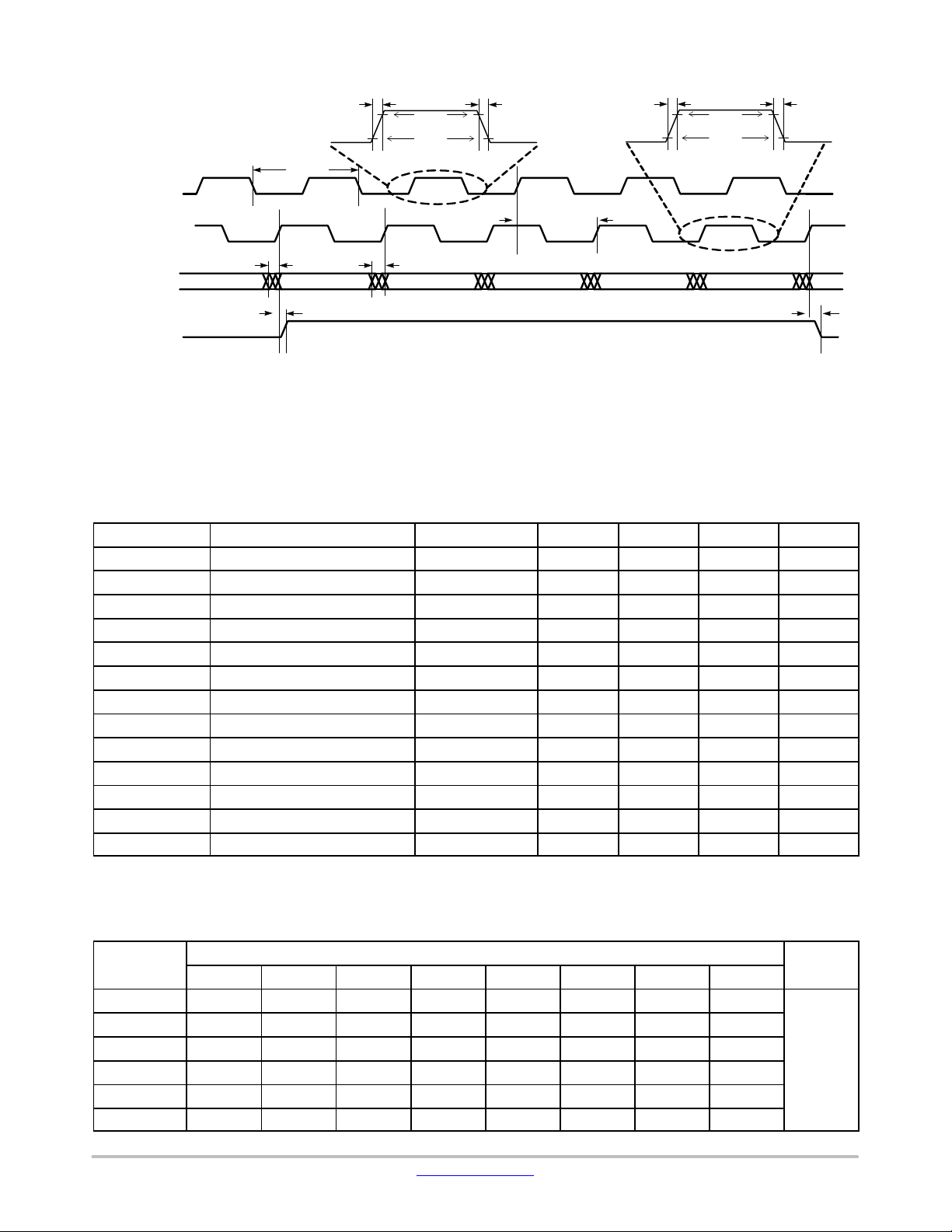
Figure 7. Two−Wire Serial Bus Timing Parameter
t
SHAW
ACK
tr_clk tf_clk
90%
10%
t
AHSW t
Register Address
Bit 7
t
AHSR
Register Value
Bit 7
t
SDHR
t
SDSR
Register Value
Register Value
Bit 0
Bit 0
90%
10%
STPS
tf_sdattr_sdat
t
STPH
www.onsemi.com
12
Page 13
AR0330CS
Table 15. TWO−WIRE SERIAL BUS CHARACTERISTICS
f
= 27 MHz; VDD = 1.8 V; VDD_IO = 2.8 V; VAA = 2.8 V; VAA_PIX = 2.8 V; VDD_PLL = 2.8 V; TA = 25°C
EXTCLK
Standard Mode Fast Mode
Parameter
SCLK Clock Frequency f
Symbol
SCL
Hold time (repeated) START condition
After this period, the first clock pulse is
generated
LOW period of the SCLK clock t
t
HD;STA
LOW
HIGH period of the SCLK clock tHIGH 4.0 − 0.6 −
Set−up time for a repeated START condi-
tSU;STA 4.7 − 0.6 −
tion
Data hold time tHD;DAT 0
Data set−up time tSU;DAT 250 − 100
Rise time of both SDATA and SCLK signals tr − 1000 20 + 0.1Cb
Fall time of both SDATA and SCLK signals tf − 300 20 + 0.1Cb
Set−up time for STOP condition tSU;STO 4.0 − 0.6 − ?s
Bus free time between a STOP and START
tBUF 4.7 − 1.3 − ?s
condition
Capacitive load for each bus line Cb − 400 − 400 pF
Serial interface input pin capacitance C
SDATA max load capacitance C
IN_SI
LOAD_SD
SDATA pull−up resistor RSD 1.5 4.7 1.5 4.7 K?
32.This table is based on I2C standard (v2.1 January 2000). Philips Semiconductor.
33.Two−wire control is I
34.All values referred to V
35. A device must internally provide a hold time of at least 300 ns for the S
36.The maximum
37.A Fast−mode I
2
C−compatible.
= 0.9 VDD and V
IHmin
t
HD;DAT has only to be met if the device does not stretch the LOW period (tLOW) of the SCLK signal.
2
C−bus device can be used in a Standard−mode I2C−bus system, but the requirement tSU; DAT 250 ns must then be met.
= 0.1VDD levels. Sensor EXCLK = 27 MHz.
ILmax
This will automatically be the case if the device does not stretch the LOW period of the S
period of the S
Standard−mode I
CLK signal, it must output the next data bit to the SDATA line
2
C−bus specification) before the SCLK line is released.
38.Cb = total capacitance of one bus line in pF.
Min Max Min Max
0 100 0 400 KHz
4.0 − 0.6 −
4.7 − 1.3 −
4
3.45
5
6
0
6
7
7
5
0.9
− ns
300 ns
300 ns
− 3.3 − 3.3 pF
− 30 − 30 pF
DATA signal to bridge the undefined region of the falling edge of SCLK.
t
r max + tSU;DAT = 1000 + 250 = 1250 ns (according to the
CLK signal. If such a device does stretch the LOW
Unit
ms
ms
ms
ms
ms
Table 16. I/O PARAMETERS
f
EXTCLK = 24 MHz; VDD = 1.8V; VAA = 2.8 V; VAA_PIX = 2.8 V; VDD_PLL = 2.8 V; Output load = 68.5 pF; TJ = 60°C; CLK_OP = 98 MPixel/s
Symbol Definition Conditions Min Max Units
VIH Input HIGH voltage
VDD_IO = 1.8 V 1.4
VDD_IO + 0.3
VDD_IO = 2.8 V 2.4
VIL Input LOW voltage
VDD_IO = 1.8 V GND – 0.3 0.4
VDD_IO = 2.8 V GND – 0.3 0.8
IIN Input leakage current No pull−up resistor; VIN = VDD OR DGND –20 20
VOH Output HIGH voltage At specified IOH VDD_IO − 0.4V – V
VOL Output LOW voltage At specified IOL – 0.4 V
IOH Output HIGH current At specified VOH – –12 mA
IOL Output LOW current At specified VOL – 9 mA
IOZ Tri−state output leakage current – 10
www.onsemi.com
13
V
mA
mA
Page 14
AR0330CS
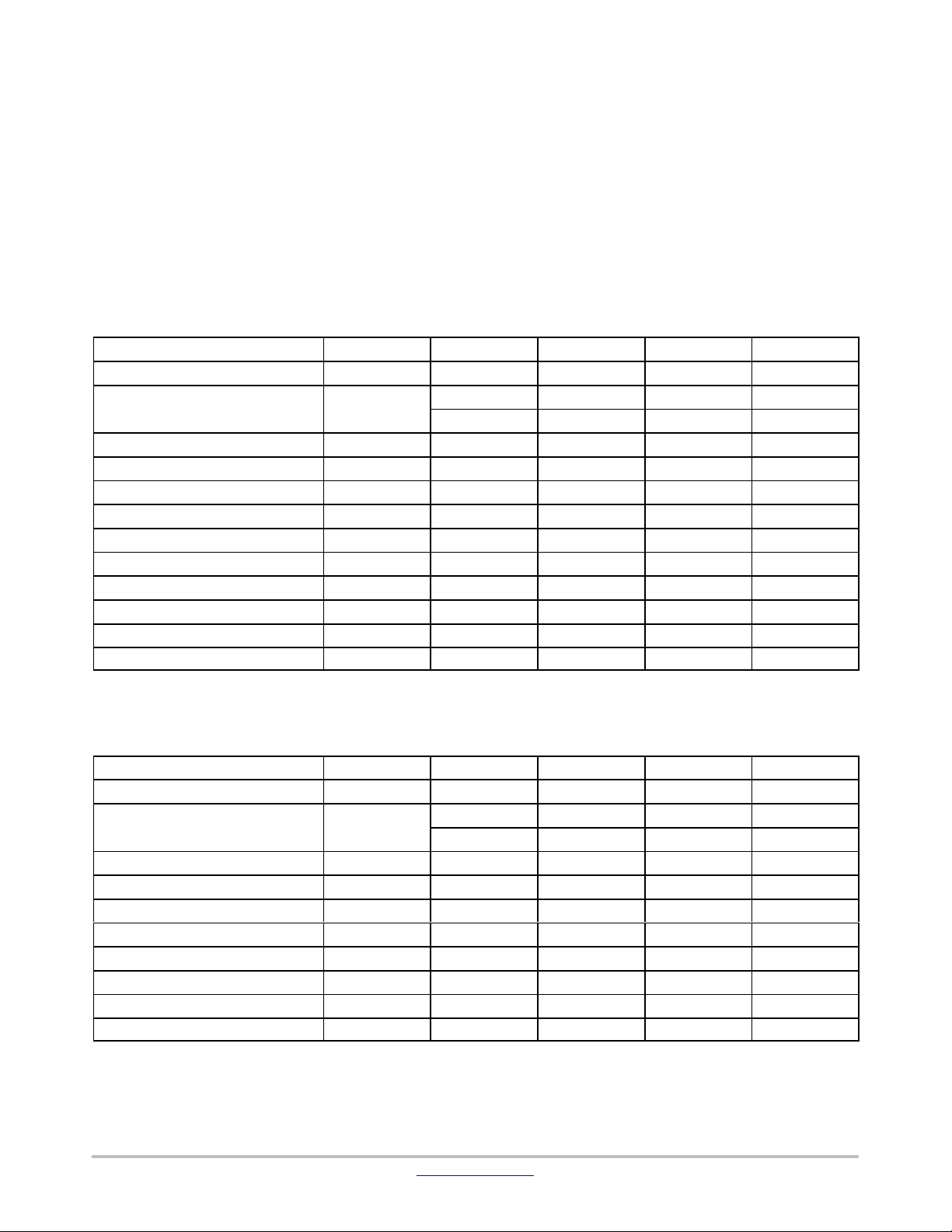
t
EXTCLK
t
R
90 %
10 %
t
F
t
RP
90 %
10 %
t
FP
EXTCLK
t
CP
PIXCLK
t
PD
FRAME_VALID trails
LINE_VALID by 16 PIXCLKs.
Data[11:0]
AME_VALID/
LINE_VALID
*PLL disabled for
t
t
CP
PD
Pxl _ 0 Pxl _ 1 Pxl _ 2 Pxl _ n
t
PFH
t
PLH
FRAME_VALID leads LINE_VALID by 609 PIXCLKs.
Figure 8. I/O Timing Diagram (Parallel Mode)
Table 17. I/O TIMING
f
EXTCLK = 24 MHz; VDD = 1.8 V; VDD_IO = 1.8 V; VAA = 2.8 V; VAA_PIX = 2.8 V; VDD_PLL = 2.8 V;
Output load = 68.5 pF; T
Symbol
fEXTCLK Input clock frequency PLL enabled 6 24 27 MHz
tEXTCLK Input clock period PLL enabled 166 41 20 ns
tR Input clock rise time 0.1 – 1 V/ns
tF Input clock fall time 0.1 – 1 V/ns
Clock duty cycle 45 50 55 %
tJITTER Input clock jitter – – 0.3 ns
Output pin slew Fastest CLOAD = 15 pF – 0.7 – V/ns
fPIXCLK PIXCLK frequency Default – 80 – MHz
tPD PIXCLK to data valid Default – – 3 ns
tPFH PIXCLK to FRAME_VALID HIGH Default – – 3 ns
tPLH PIXCLK to LINE_VALID HIGH Default – – 3 ns
tPFL PIXCLK to FRAME_VALID LOW Default – – 3 ns
tPLL PIXCLK to LINE_VALID LOW Default – – 3 ns
= 60°C; CLK_OP = 98 MPixel/s
J
Definition Conditions Min Typ Max Units
t
PFL
t
PLL
Table 18. PARALLEL I/O RISE SLEW RATE
f
EXTCLK = 24 MHz; VDD = 1.8 V; VAA = 2.8 V; VAA_PIX = 2.8 V; VDD_PLL = 2.8 V; Output load = 68.5 pF;
= 60°C; CLK_OP = 98 MPixel/s
T
J
Parallel Slew Rate (R0x306E[15:13])
V
DD_IO
0 1 2 3 4 5 6 7
1.70V 0.069 0.115 0.172 0.239 0.325 0.43 0.558 0.836
1.80V 0.078 0.131 0.195 0.276 0.375 0.507 0.667 1.018
1.95V 0.093 0.156 0.233 0.331 0.456 0.62 0.839 1.283
2.50V 0.15 0.252 0.377 0.539 0.759 1.07 1.531 2.666
2.80V 0.181 0.305 0.458 0.659 0.936 1.347 1.917 3.497
3.10V 0.212 0.361 0.543 0.78 1.114 1.618 2.349 4.14
www.onsemi.com
14
Units
V/ns
Page 15
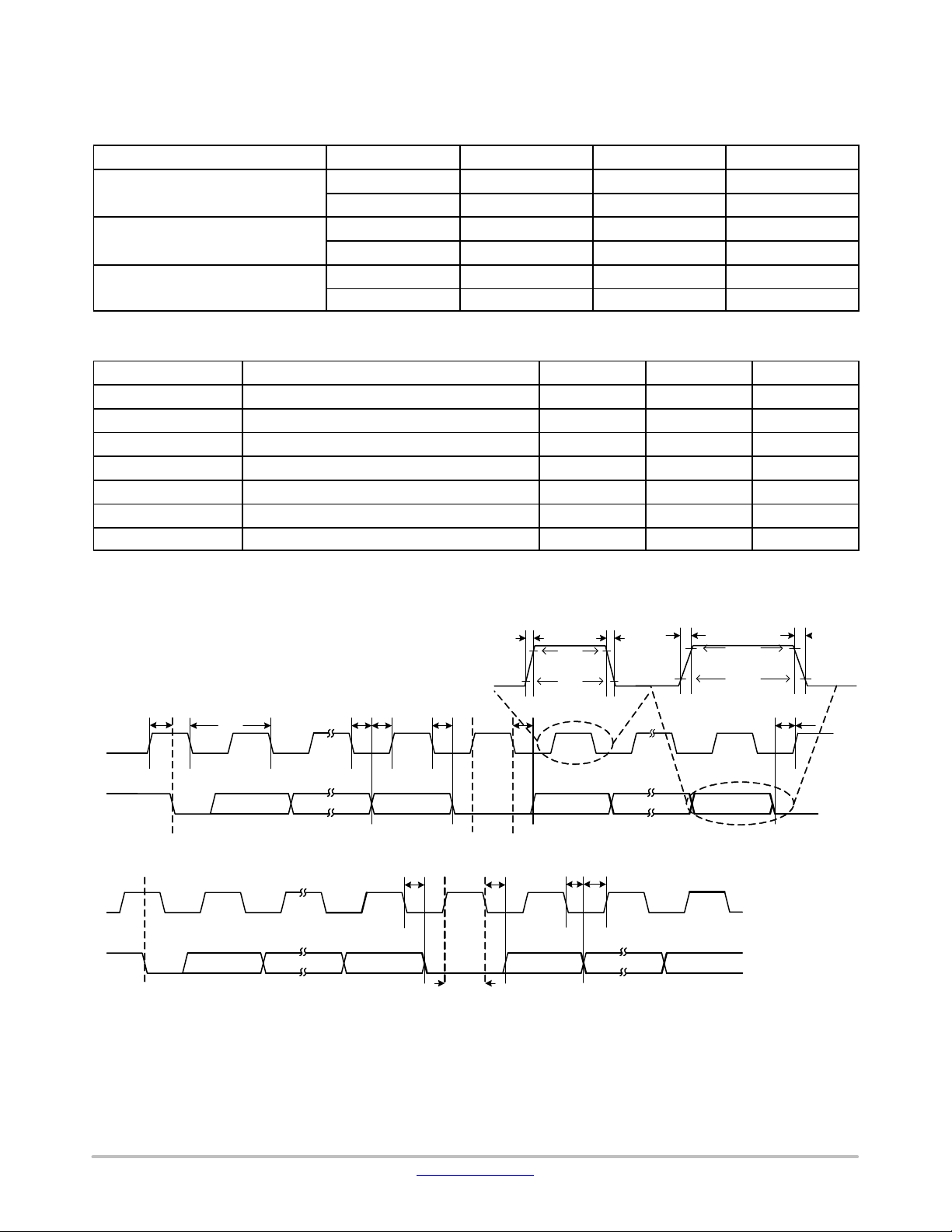
ELECTRICAL DEFINITIONS
Figure 9 is the diagram defining differential amplitude
V
, V
OD
V
CM
Single−ended signal
and rise and fall times. To measure VOD and
CM,
use the DC test circuit shown in Figure 10 and set the
V
o a
V
V
o b
Differential signal
0 V
O D_ A C
V
diff
V
OD
|V
o b
V
O D
=
– V
|
o a
AR0330CS
MIPI PHY to constant Logic 1 and Logic 0. Measure V
V
and VCM with voltmeters for both Logic 1 and Logic 0.
ob
R
t
V
diff
V
O D
|V
o a
_ pkpk
– V
,
oa
V
= (V
C M
8 0%
=
|
o b
t
F
2 0%
o a
+ V
o b
) / 2
Figure 9. Single−Ended and Differential Signals
V
o a
V
V
o b
5 0 Ω
5 0 Ω
V
C M
V
Figure 10. DC Test Circuit
VOD(m) +ŤVoa(m) * Vob(m)Ťwhere ȀmȀ is either ″ 1″ for logic 1 or ″ 0″ for logic 0
V
(1) ) VOD(0)
OD
+
V
OD
V
+ VOD(1) ) VOD(0)
diff
DVOD+ŤVOD(1) * VOD(0)
2
Ť
(eq. 1)
(eq. 2)
(eq. 3)
(eq. 4)
V
(1) ) VCM(0)
CM
+
V
CM
2
www.onsemi.com
15
(eq. 5)
Page 16

AR0330CS
DV
CM
Both VOD and VCM are measured for all output channels.
The worst case
V
between all channels regardless of logic level. And the
OD
worst case
difference in V
DV
is defined as the largest difference in
OD
DV
is similarly defined as the largest
CM
between all channels regardless of logic
CM
level.
Timing Definitions
1. Timing measurements are to be taken using the
Square Wave test mode
2. Rise and fall times are measured between 20% to
80% positions on the differential waveform, as
t
pw
Clock
Data
1 UI
0.5 UI
t
+ŤVCM(1) * VCM(0)
3. Mean Clock−to−Data skew should be measured
t
CHSKEW
Ť
(eq. 6)
shown in Figure 9: “Single−Ended and Differential
Signals”
from the 0V crossing point on Clock to the 0V
crossing point on any Data channel regardless of
edge, as shown in Figure 11. This time is
compared with the ideal Data transition point of
0.5UI with the difference being the Clock−to−Data
Skew (see Equation 7)
Figure 11. Clock−to−Data Skew Timing Diagram
t
t
4. The differential skew is measured on the two
single−ended signals for any channel. The time is
taken from a transition on V
Common−mode AC Signal
signal to
oa
V
CHSKEW
CHSKEW
CM_AC
(ps) + Dt *
Dt
(UI) +
t
pw
t
pw
2
* 0.5
corresponding transition on V
crossing point
t
DIFFSKEW
V
CM_AC
(eq. 7)
(eq. 8)
signal at V
ob
V
CM
V
CM
CM
Figure 12. Differential Skew
www.onsemi.com
16
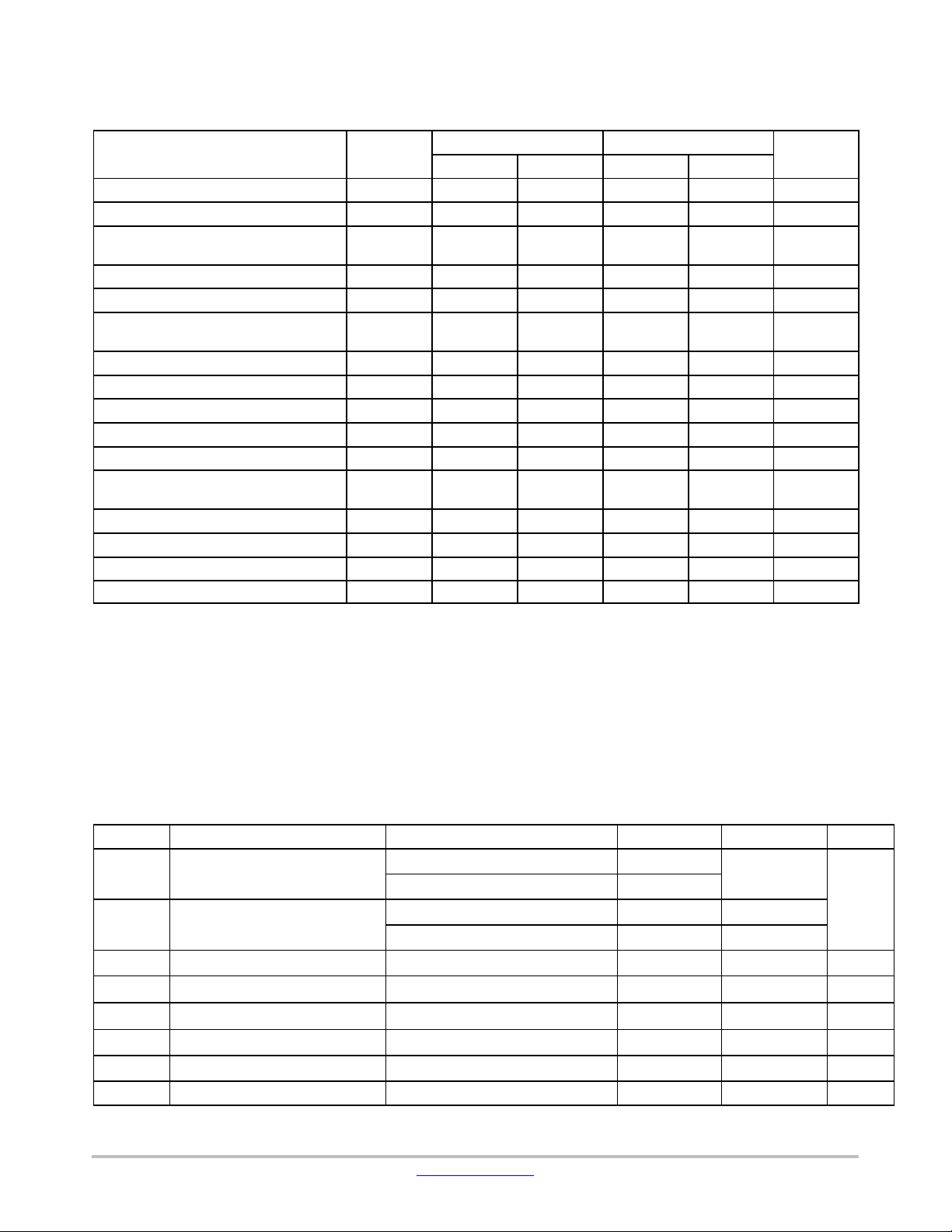
Page 17

AR0330CS
Figure 12 also shows the corresponding AC V
CM
common−mode signal. Differential skew between the V
and Vob signals can cause spikes in the common−mode,
which the receiver needs to be able to reject. V
1.3 * V
OD
V
OD
0.7 * V
OD
0
Differential Amplitude
*0.7 * V
OD
*V
OD
*1.3 * V
OD
t
CM_AC
PRE
is
oa
Eye Width
measured as the absolute peak deviation from the mean DC
V
common−mode.
CM
Transmitter Eye Mask
Eye Height
t
POST
0 0.2 0.37 0.5 0.63 10.8
Normalized Time
Figure 13. Transmitter Eye Mask
Figure 13 defines the eye mask for the transmitter. 0.5 UI
point is the instantaneous crossing point of the Clock. The
area in white shows the area Data is prohibited from crossing
into. The eye mask also defines the minimum eye height, the
data t
skew (t
and t
pre
TJSKEW
times, and the total jitter pk−pk +mean
post
) for Data.
Clock
Figure 14. Clock Duty Cycle
t
HCLK
D
CYC
D
CYC
t
+
pw
Bitrate +
Clock Signal
t
is defined as the high clock period, and t
HCLK
defined as the low clock period as shown in Figure 14. The
clock duty cycle D
clock is either high (t
is defined as the percentage time the
CYC
HCLK
) or low (t
) compared with
LCLK
the clock period T.
t
LCLK
t
HCLK
(1) +
T
t
LCLK
(0) +
T
T
(i.e, 1 UI)
2
1
t
pw
LCLK
(eq. 9)
(eq. 10)
(eq. 11)
(eq. 12)
is
www.onsemi.com
17
Page 18

Figure 15 shows the definition of clock jitter for both the
period and the cycle−to−cycle jitter.
AR0330CS
t
HCLK
t
pw
Figure 15. Clock Jitter
Period Jitter (t
instantaneous clock t
measured for both the clock high period variation
and the clock low period variation Dt
) is defined as the deviation of the
CKJIT
from an ideal 1UI. This should be
PW
taking the RMS
LCLK
Dt
HCLK,
SEQUENCER
The sequencer digital block determines the order and
timing of operations required to sample pixel data from the
array during each row period. It is controlled by an
instruction set that is programmed into RAM from the
sensor OTPM (One Time Programmable Memory). The
OTPM is configured during production.
The instruction set determines the length of the sequencer
operation that determines the “ADC Readout Limitation”
(Equation 5) listed in the Sensor Frame−Rate section. The
instruction set can be shortened through register writes in
order to achieve faster frame rates. Instructions for
shortening the sequencer can be found in the AR0330CS
Developer Guide.
The sequencer digital block can be reprogrammed using
the following instructions:
t
LCLK
(RMS)
t
CKJIT
or 1−sigma standard deviation and quoting the worse case
jitter between
Dt
HCLK
and Dt
LCLK
.
If pk−pk jitter is also measured, this should be limited to
±3−sigma.
Program a new sequencer.
1. Place the sensor in standby
2. Write 0x8000 to R0x3088 (“seq_ctrl_port”)
3. Write each instruction incrementally to R0x3086
Each write must be 16−bit consisting of two bytes
{Byte[N], Byte[N+1]}
4. If the sequencer consists of an odd number of
bytes, set the last byte to “0”
Read the instructions stored in the sequencer.
1. Place the sensor in standby
2. Write 0xC000 to R0x3088 (“seq_ctrl_port”)
3. Sequentially read 2−bytes at a time from R0x3086
www.onsemi.com
18
Page 19

SENSOR PLL
VCO
AR0330CS
EXTCLK
(6−27 MHz)
pre_pll_clk_div
2 (1−64)
Figure 16. Relationship Between Readout Clock and Peak Pixel Rate
The sensor contains a phase−locked loop (PLL) that is
used for timing generation and control. The required VCO
clock frequency is attained through the use of a pre−PLL
clock divider followed by a multiplier. The multiplier is
followed by set of dividers used to generate the output clocks
CLK_PIX
All Digital
Blocks
Pixel Array
pll_multiplier
58 (32−384)
required for the sensor array, the pixel analog and digital
readout paths, and the output parallel and serial interfaces.
Dual Readout Paths
There are two readout paths within the sensor digital
block.
S erial Output
(MIPI or Parallel)
Pixel Rate = 2 x CLK_PIX
= # data lanes x CLK_OP
(Parallel or MIPI)
= CLK_OP (Parallel)
F
VCO
All Digital
Blocks
CLK_PIX
Figure 17. Sensor Dual Readout Paths
The sensor row time calculations refers to each data−path
individually. For example, the sensor default configuration
uses 1248 clocks per row (line_length_pck) to output 2304
F
V C O
E X T C L K
( 6−27 MHz)
pre_pll_clk_div
2 (1−64)
pll_multiplier
58 (32 − 384)
Figure 18. PLL for the Parallel Interface
active pixels per row. The aggregate clocks per row seen by
the receiver will be 2496 clocks (1248 x 2 readout paths).
Parallel PLL Configuration
vt_sys_clk_div
1 ( 1, 2, 4, 6, 8,
10, 12, 14, 16)
vt_pix_clk_div
6 (4−16)
1/2
CLK_OP
(Max 98 MPixel/s)
CLK_PIX
(Max 49 MPixels/s)
www.onsemi.com
19
Page 20

AR0330CS
The maximum output of the parallel interface is 98
Mpixel/s (CLK_OP). This will limit the readout clock
(CLK_PIX) to 49 MHz. The sensor will not use the F
F
SERIAL_CLK
when configured to use the parallel interface.
Table 19. PLL PARAMETERS FOR THE PARALLEL INTERFACE
Parameter Symbol Min Max Unit
External Clock EXTCLK 6 27 MHz
VCO Clock F
VCO
384 768 MHz
Readout Clock CLK_PIX 49 MHz
Output Clock CLK_OP 98 Mpixel/s
Table 20. EXAMPLE PLL CONFIGURATION FOR THE PARALLEL INTERFACE
Parameter Value Output
F
VCO
588 MHz (Max)
vt_sys_clk_div 1
vt_pix_clk_div 6
CLK_PIX 49 MHz (CLK_OP/2)
CLK_OP 98 Mpixel/s (= 588 MHz / 6)
Output pixel rate 98 MPixel/s
Serial PLL Configuration
SERIAL
,
E X T C L K
( 6−27 MHz)
pre_pll_clk_div
2 (1−64)
pll_multiplier
58 (32 − 384)
Figure 19. PLL for the Serial Interface
The sensor will use op_sys_clk_div and op_pix_clk_div
to configure the output clock per lane (CLK_OP). The
configuration will depend on the number of active lanes (1
F
F
V C O
V C O
vt_sys_clk_div
1 ( 1, 2, 4, 6, 8,
10, 12, 14, 16)
op_sys_clk_div
(constant = 1)
vt_pix_clk_div
6 (4−16)
op_pix_clk_div
12 (8, 10, 12)
1/2
F
or 2) configured. To configure the sensor protocol and
number of lanes, refer to “Serial Configuration”.
C L K_P IX
C L K _O P
F
S E R IA L
S E R IA L _C L K
www.onsemi.com
20
Page 21

AR0330CS
Table 21. PLL PARAMETERS FOR THE SERIAL INTERFACE
Parameter Symbol Min Max Unit
External Clock EXTCLK 6 27 MHz
VCO Clock F
Readout Clock CLK_PIX 98 MHz
Output Clock CLK_OP 98 Mpixel/s
Output Serial Data Rate Per Lane
Output Serial Clock Speed Per Lane
VCO
F
SERIAL
F
SERIAL_CLK
384 768 MHz
384 (MIPI) 768 (MIPI) Mbps
192 (MIPI) 384 (MIPI) MHz
The serial output should be configured so that it adheres
to the following rules:
• The maximum data−rate per lane (F
SERIAL
) is
768 Mbps/lane (MIPI)
• The output pixel rate per lane (CLK_OP) should be
configured so that the sensor output pixel rate matches
the peak pixel rate (2 x CLK_PIX)
♦ 2−lane: 2 x CLK_OP = 2 x CLK_PIX = Pixel Rate
♦ 1−lane: 1 x CLK_OP = 2 x CLK_PIX = Pixel Rate
Table 22. EXAMPLE PLL CONFIGURATIONS FOR THE SERIAL INTERFACE
2−lane 1−lane
Parameter
F
VCO
vt_sys_clk_div 2 2 4 4 4
vt_pix_clk_div 6 5 6 5 4
op_sys_clk_div 1 1 1 1 1
op_pix_clk_div 12 10 12 10 8
F
SERIAL
F
SERIAL_CLK
CLK_PIX 64 76 32 38.4 48 MHz
CLK_OP 64 76 64 76.8 96 Mpixel/s
Pixel Rate 128 144 64 76.8 96 Mpixel/s
12−bit 10−bit 12−bit 10−bit 8−bit
768 760 768 768 768 MHz
768 760 768 768 768 MHz
384 380 384 384 384 MHz
Notes
PIXEL OUTPUT INTERFACES
Parallel Interface
The parallel pixel data interface uses these output−only
signals:
• FV
• LV
• PIXCLK
• DOUT[11:0]
The parallel pixel data interface is disabled by default at
power up and after reset. It can be enabled by programming
R0x301A. Table 24 shows the recommended settings.
www.onsemi.com
When the parallel pixel data interface is in use, the serial
data output signals can be left unconnected. Set
reset_register[12] to disable the serializer while in parallel
output mode.
Output Enable Control
When the parallel pixel data interface is enabled, its
signals can be switched asynchronously between the driven
and High−Z under pin or register control, as shown in
Table 23.
21
Page 22

AR0330CS
Table 23. OUTPUT ENABLE CONTROL
OE_BAR Pin Drive Signals R0x301A–B[6] Description
Disabled 0 Interface High−Z
Disabled 1 Interface driven
1 0 Interface High−Z
X 1 Interface driven
0 X Interface driven
Configuration of the Pixel Data Interface
Fields in R0x301A are used to configure the operation of
the pixel data interface. The supported combinations are
shown in Table 23.
Table 24. CONFIGURATION OF THE PIXEL DATA INTERFACE
Serializer
Disable
R0x301
A–B[12]
0 0 1 Power up default.
1 1 0 Parallel pixel data interface, sensor core data output. Serial pixel data interface
1 1 1 Parallel pixel data interface, sensor core data output. Serial pixel data interface
Parallel
Enable
R0x301A–B[7]
Standby
End−of−Frame
R0x301A–B[4]
Description
Serial pixel data interface and its clocks are enabled. Transitions to soft
standby are synchronized to the end of frames on the serial pixel data
interface
and its clocks disabled to save power. Transitions to soft standby are
synchronized to the end of the current row readout on the parallel pixel data
interface
and its clocks disabled to save power. Transitions to soft standby are
synchronized to the end of frames in the parallel pixel data interface
MIPI Interface
The serial pixel data interface uses the following
output−only signal pairs:
• DATA1_P
• DATA1_N
• DATA2_P
• DATA2_N
• CLK_P
• CLK_N
The signal pairs use both single−ended and differential
signaling, in accordance with the the MIPI Alliance
Specification for D−PHY v1.00.00. The serial pixel data
interface is enabled by default at power up and after reset.
The DATA0_P, DATA0_N, DATA1_P, DATA1_N,
CLK_P and CLK_N pads are set to the Ultra Low Power
State (ULPS) if the serial disable bit is asserted
(R0x301A−B[12] = 1) or when the sensor is in the hardware
standby or soft standby system states.
When the serial pixel data interface is used, the
LINE_VALID, FRAME_VALID, PIXCLK and
D
OUT[11:0] signals (if present) can be left unconnected.
Serial Configuration
The serial format should be configured using R0x31AC.
This register should be programmed to 0x0C0C when using
the parallel interface.
The R0x0112−3 register can be programmed to any of the
following data format settings that are supported:
• 0x0C0C – Sensor supports RAW12 uncompressed data
format
• 0x0C0A – The sensor supports RAW12 compressed
format (10−bit words) using 12−10 bit A−LAW
Compression. See “Compression”
• 0x0A0A – Sensor supports RAW10 uncompressed data
format. This mode is supported by discarding all but the
upper 10 bits of a pixel value
• 0x0808 – Sensor supports RAW8 uncompressed data
format. This mode is supported by discarding all but the
upper 8 bits of a pixel value (MIPI only)
The serial_format register (R0x31AE) register controls
which serial interface is in use when the serial interface is
www.onsemi.com
22
Page 23

AR0330CS
enabled (reset_register[12] = 0). The following serial
formats are supported:
• 0x0201 – Sensor supports single−lane MIPI operation
• 0x0202 – Sensor supports dual−lane MIPI operation
The MIPI timing registers must be configured differently
for 10−bit or 12−bit modes. These modes should be
configured when the sensor streaming is disabled. See
Table 25.
• 0x0A0A – Sensor supports RAW10 uncompressed data
format. This mode is supported by discarding all but the
upper 10 bits of a pixel value
• 0x0808 – Sensor supports RAW8 uncompressed data
format. This mode is supported by discarding all but the
upper 8 bits of a pixel value (MIPI only)
Table 25. RECOMMENDED MIPI TIMING CONFIGURATION
Configuration
10−bit, 490 Mbps/lane 12−bit, 588 Mbps/lane
Register
0x31B0 40 36 Frame Preamble
0x31B2 14 12 Line Preamble
0x31B4 0x2743 0x2643 MIPI Timing 0
0x31B6 0x114E 0x114E MIPI Timing 1
0x31B8 0x2049 0x2048 MIPI Timing 2
0x31BA 0x0186 0x0186 MIPI Timing 3
0x31BC 0x8005 0x8005 MIPI Timing 4
0x31BE 0x2003 0x2003 MIPI Config Status
Clocking: Continuous
The serial_format register (R0x31AE) register controls
which serial interface is in use when the serial interface is
enabled (reset_register[12] = 0). The following serial
formats are supported:
• 0x0201 – Sensor supports single−lane MIPI operation
• 0x0202 – Sensor supports dual−lane MIPI operation
The MIPI timing registers must be configured differently
for 10−bit or 12−bit modes. These modes should be
configured when the sensor streaming is disabled. See
Table 25.
Description
PIXEL SENSITIVITY
Row Integration
Row Reset
(Start of integration)
Figure 20. Integration Control in ERS Readout
A pixel’s integration time is defined by the number of
clock periods between a row’s reset and read operation. Both
the read followed by the reset operations occur within a row
period (T
) where the read and reset may be applied to
ROW
different rows. The read and reset operations will be applied
to the rows of the pixel array in a consecutive order.
The integration time in an ERS frame is defined as:
(T
INTEGRATION
)
Row Readout
T
INTEGRATION
+ T
COARSE
* T
FINE
The coarse integration time is defined by the number of
row periods (T
) between a row’s reset and the row read.
ROW
The row period is the defined as the time between row read
operations (see Sensor Frame Rate).
T
COARSE
+ T
coarse_inegration_time
ROW
(eq. 13)
(eq. 14)
www.onsemi.com
23
Page 24

AR0330CS
Vertical Blanking
T
COARSE
8.33 ms = 654 rows x 12.7 ms/row
= coarse_integration_time x T
ROW
Read
Reset
Horizontal Blanking
Figure 21. Example of 8.33 ms Integration in 16.6 ms Frame
The fine integration is then defined by the number of pixel
clock periods between the row reset and row read operation
Start of Read Row N
and Reset Row K
Read Row N Reset Row K
T
= fine_integration _time x (1/CLK_PIX)
FINE
T
= line_length _pck x (1/CLK_PIX)
ROW
Vertical Blanking
within T
. This period is defined by the
ROW
fine_integration_time register.
T
= frame_length_lines x T
FRAME
16.6 ms = 1308 rows x 12.7 ms/row
Time
Start of Read Row N + 1
and Reset Row K + 1
ROW
Figure 22. Row Read and Row Reset Showing Fine Integration
T
+ fine_inegration_timeńclk_pix
FINE
The maximum allowed value for fine_integration_time is
line_length_pck − 1204.
T
= coarse_integration_time x T
COARSE ROW
20.7 ms = 1634 rows x 12.7 ms/row
Time
Read
Pointer
Shutter
Pointer
ON Semiconductor recommends that the
fine_integration_time in the AR0330CS be left at zero.
Vertical Blanking
Image
Horizontal Blanking
Vertical Blanking
Extended Vertical Blanking
Image
(eq. 15)
= frame_length_lines x T
T
FRAME
16.6 ms = 1308 rows x 12.7 ms/row
4.1 ms
ROW
Horizontal Blanking
Figure 23. The Row Integration Time is Greater Than the Frame Readout Time
www.onsemi.com
24
Page 25

AR0330CS
The minimum frame−time is defined by the number of
row periods per frame and the row period. The sensor
frame−time will increase if the coarse_integration_time is
set to a value equal to or greater than the frame_length_lines.
The maximum integration time can be limited to the frame
time by setting R0x30CE[5] to 1.
www.onsemi.com
25
Page 26

AR0330CS
GAIN STAGES
The analog gain stages of the AR0330CS sensor are
shown in Figure 24. The sensor analog gain stage consists of
column amplifiers and a variable ADC reference. The sensor
will apply the same analog gain to each color channel.
Digital gain can be configured to separate levels for each
color channel.
ADC
Reference
Coarse Gain:
1x, 2x, 4x, 8x
Fine Gain:
1−2x: 16 steps
2−4x: 8 steps
4−8x: 4 steps
Digital Gain
with Dithering
1x to 15.992x
(128 steps per 6dB)
“xxxx.Yyyy”
xxxx(15−0)
yyyyyyy( 127/128 to 0)
Figure 24. Gain Stages in AR0330CS Sensor
The level of analog gain applied is controlled by the
coarse_gain and fine_gain registers. The analog readout can
be configured differently for each gain level. The
recommended gain tables are listed in Table 26. It is
recommended that these registers are configured before
streaming images.
Table 26. RECOMMENDED SENSOR ANALOG GAIN TABLES
COARSE_GAIN FINE_GAIN Total Gain COARSE_GAIN FINE_GAIN Total Gain
R0x3060
[5:4]
0 1 0 1.00 1.00 0.00 0 1x 15 1.88 1.88 5.49
0 1 1 1.03 1.03 0.26 1 2x 0 1.00 2.00 6.00
0 1 2 1.07 1.07 0.56 1 2x 2 1.07 2.13 6.58
0 1 3 1.10 1.10 0.86 1 2x 4 1.14 2.29 7.18
0 1 4 1.14 1.14 1.16 1 2x 6 1.23 2.46 7.82
0 1 5 1.19 1.19 1.46 1 2x 8 1.33 2.67 8.52
0 1 6 1.23 1.23 1.80 1 2x 10 1.45 2.91 9.28
0 1 7 1.28 1.28 2.14 1 2x 12 1.60 3.20 10.10
0 1 8 1.33 1.33 2.50 1 2x 14 1.78 3.56 11.02
0 1 9 1.39 1.39 2.87 2 4x 0 1.00 4.00 12.00
0 1 10 1.45 1.45 3.25 2 4x 4 1.14 4.57 13.20
0 1 11 1.52 1.52 3.66 2 4x 8 1.33 5.33 14.54
0 1 12 1.60 1.60 4.08 2 4x 12 1.60 6.40 16.12
0 1 13 1.68 1.68 4.53 3 8x 0 1.00 8.00 18.00
0 1 14 1.78 1.78 5.00
Gain
(x)
R0x3060[3:0]
Gain
(x)
(x) (dB) R0x3060 [5:4]
Gain
(x)
R0x3060
[3:0]
Gain
(x)
(x) (dB)
Each digital gain can be configured from a gain of 0 to
15.992. The digital gain supports 128 gain steps per 6dB of
gain. The format of each digital gain register is
“xxxx.yyyyyyy” where “xxxx” refers an integer gain of 1 to
15 and “yyyyyyy” is a fractional gain ranging from 0/128 to
127/128.
www.onsemi.com
The sensor includes a digital dithering feature to reduce
quantization resulting from using digital gain can be
implemented by setting R0x30BA[5] to 1. The default value
is 0. Refer to “Real−Time Context Switching” for the analog
and digital gain registers in both context A and context B
modes.
26
Page 27

AR0330CS
Refer to “Real−Time Context Switching” for the analog
and digital gain registers in both context A and context B
modes.
www.onsemi.com
27
Page 28

AR0330CS
DATA PEDESTAL
The data pedestal is a constant offset that is added to pixel
values at the end of datapath. The default offset is 168 and
is a 12−bit offset. This offset matches the maximum range
used by the corrections in the digital readout path.
SENSOR READOUT
Image Acquisition Modes
The AR0330CS supports two image acquisition modes:
1. Electronic rolling shutter (ERS) mode
This is the normal mode of operation. When the
AR0330CS is streaming; it generates frames at a
fixed rate, and each frame is integrated (exposed)
using the ERS. When the ERS is in use, timing
and control logic within the sensor sequences
through the rows of the array, resetting and then
reading each row in turn. In the time interval
between resetting a row and subsequently reading
that row, the pixels in the row integrate incident
light. The integration (exposure) time is controlled
by varying the time between row reset and row
readout. For each row in a frame, the time between
row reset and row readout is the same, leading to a
uniform integration time across the frame. When
the integration time is changed (by using the
two−wire serial interface to change register
settings), the timing and control logic controls the
transition from old to new integration time in such
a way that the stream of output frames from the
AR0330CS switches cleanly from the old
integration time to the new while only generating
frames with uniform integration. See “Changes to
The data pedestal value can be changed if the lock register
bit (R0x301A[3]) is set to “0”. This bit is set to “1” by
default.
Integration Time” in the AR0330CS Register
Reference
2. Global reset mode
This mode can be used to acquire a single image at
the current resolution. In this mode, the end point
of the pixel integration time is controlled by an
external electromechanical shutter, and the
AR0330CS provides control signals to interface to
that shutter.
The benefit of using an external electromechanical
shutter is that it eliminates the visual artifacts
associated with ERS operation. Visual artifacts
arise in ERS operation, particularly at low frame
rates, because an ERS image effectively integrates
each row of the pixel array at a different point in
time
Window Control
The sequencing of the pixel array is controlled by the
x_addr_start, y_addr_start, x_addr_end, and y_addr_end
registers. The x_addr_start equal to 6 is the minimum setting
value. The y_addr_start equal to 6 is the minimum setting
value. Please refer to Table 27 and Table 28 for details.
Table 27. PIXEL COLUMN CONFIGURATION
Column Address Number Type Notes
0–5 6 Active Border columns
6–2309 2304 Active Active columns
2310–2315 6 Active Border columns
Table 28. PIXEL ROW CONFIGURATION
Row Address Number Type Notes
2–5 4 Active Not used in case of “edge effects”
6–1549 1544 Active Active rows
1550–1555 6 Active Not used in case of “edge effects”
www.onsemi.com
28
Page 29

AR0330CS
Readout Modes
Horizontal Mirror
When the horizontal_mirror bit (R0x3040[14]) is set in
the image_orientation register, the order of pixel readout
within a row is reversed, so that readout starts from
x_addr_end + 1and ends at x_addr_start. Figure 25 shows a
LINE_VALID
sequence of 6 pixels being read out with R0x3040[14] = 0
and R0x3040[14] = 1. Changing R0x3040[14] causes the
Bayer order of the output image to change; the new Bayer
order is reflected in the value of the pixel_order register.
horizontal_mirror = 0
[11:0]
D
OUT
horizontal_mirror = 1
[11:0]
D
OUT
Figure 25. Effect of Horizontal Mirror on Readout Order
G0[11:0] R0[11:0] G1[11:0] R1[11:0] G2[11:0] R2[11:0]
G3[11:0] R2[11:0] G2[11:0] R1[11:0] G1[11:0] R0[11:0]
Vertical Flip
When the vertical_flip bit (R0x3040[15]) is set in the
image_orientation register, the order in which pixel rows are
read out is reversed, so that row readout starts from
y_addr_end and ends at y_addr_start. Figure 30 shows a
FRAME_VALID
vertical_flip = 0
DOUT[11:0]
vertical_flip = 1
DOUT[11:0]
Row0[11:0] Row1[11:0] Row2[11:0] Row3[11:0] Row4[11:0] Row5[11:0]
Row6[11:0] Row5[11:0] Row4[11:0] Row3[11:0] Row2[11:0] Row1[11:0]
Figure 26. Effect of Vertical Flip on Readout Order
sequence of 6 rows being read out with R0x3040[15] = 0 and
R0x3040[15] = 1. Changing this bit causes the Bayer order
of the output image to change; the new Bayer order is
reflected in the value of the pixel_order register.
SUBSAMPLING
The AR0330CS supports subsampling. Subsampling
allows the sensor to read out a smaller set of active pixels by
either skipping or binning pixels within the readout window.
Isb
Isb
Figure 27. Horizontal Binning in the AR0330CS Sensor
Horizontal binning is achieved either in the pixel readout
or the digital readout. The sensor will sample the combined
2x or 3x adjacent pixels within the same color plane.
www.onsemi.com
The working modes described in the data sheet that use
subsampling are configured to use either 2x2 or 3x3
subsampling.
29
Page 30

AR0330CS
*
e
*
e
Figure 28. Vertical Row Binning in the AR0330CS Sensor
Vertical row binning is applied in the pixel readout. Row
binning can be configured of 2x rows within the same color
plane.
Pixel skipping can be configured up to 2x and 3x in both
the x−direction and y−direction. Skipping pixels in the
x−direction will not reduce the row time. Skipping pixels in
the y−direction will reduce the number of rows from the
sensor effectively reducing the frame time. Skipping will
introduce image artifacts from aliasing.
The sensor increments its x and y address based on the
x_odd_inc and y_odd_inc value. The value indicates the
addresses that are skipped after each pair of pixels or rows
has been read.
The sensor will increment x and y addresses in multiples
of 2. This indicates that a GreenR and Red pixel pair will be
Table 29. CONFIGURATION FOR HORIZONTAL SUBSAMPLING
x_odd_inc Restrictions:
No subsampling x_odd_inc = 1
skip = (1 + 1) × 0.5 = 1x
Skip 2x x_odd_inc = 3
skip = (1 + 3) × 0.5 = 2x
Skip 3x x_odd_inc = 5
skip = (1 + 5) × 0.5 = 3x
Analog Bin 2x x_odd_inc = 3
skip = (1 + 3) × 0.5 = 2x
col_sf_bin_en = 1
The horizontal FOV must be programmed to meet the following rule:
read together. As well, that the sensor will read a Gr−R row
first followed by a B−Gb row.
x subsampling factor +
y subsampling factor +
1 ) x_odd_inc
2
1 ) y_odd_inc
2
(eq. 16)
(eq. 17)
A value of 1 is used for x_odd_inc and y_odd_inc when
no pixel subsampling is indicated. In this case, the sensor is
incrementing x and y addresses by 1 + 1 so that it reads
consecutive pixel and row pairs. To implement a 2x skip in
the x direction, the x_odd_inc is set to 3 so that the x address
increment is 1 + 3, meaning that sensor will skip every other
Gr−R pair.
x_addr_end * x_addr_start ) 1
(x_odd_inc ) 1)ń2
+ even number
Digital Bin 2x x_odd_inc = 3
skip = (1+3) × 0.5 = 2x
col_bin = 1
Digital Bin 3x x_odd_inc = 5
skip = (1 + 5) × 0.5 = 3x
col_bin = 1
www.onsemi.com
30
Page 31

AR0330CS
Table 30. CONFIGURATION FOR VERTICAL SUBSAMPLING
y_odd_inc Restrictions:
No subsampling y_odd_inc = 1
skip = (1 + 1) × 0.5 = 1x
row_bin = 0
Skip 2x y_odd_inc = 3
skip = (1 + 3) × 0.5 = 2x
row_bin = 0
Skip 3x y_odd_inc = 5
skip = (1 + 5) × 0.5 = 3x
row_bin = 0
Analog Bin 2x y_odd_inc = 3
skip = (1 + 3) × 0.5 = 2x
row_bin = 1
The horizontal FOV must be programmed to meet the following rule:
y_addr_end * y_addr_start ) 1
(y_odd_inc ) 1)ń2
+ even number
www.onsemi.com
31
Page 32

AR0330CS
SENSOR FRAME RATE
The time required to read out an image frame (T
FRAME
can be derived from the number of clocks required to output
each image and the pixel clock.
The frame−rate is the inverse of the frame period.
fps + 1ńT
FRAME
(eq. 1)
The number of clocks can be simplified further into the
following parameters:
• The number of clocks required for each sensor row
(line_length_pck)
T
+ 1ń(CLK_PIX) [frame_length_lines line_lenght_pck ) extra_delay)
FRAME
)
This parameter also determines the sensor row period
when referenced to the sensor readout clock.
= line_length_pck x 1/CLK_PIX)
(T
ROW
• The number of row periods per frame
(frame_length_lines)
• An extra delay between frames used to achieve a
specific output frame period (extra_delay)
Vertical Blanking (VB)
Active Rows
(eq. 2)
Horizontal
Blanking
(HB)
Figure 29. Frame Period Measured in Clocks
Row Period (T
ROW
)
The line_length_pck will determine the number of clock
periods per row and the row period (T
) when combined
ROW
with the sensor readout clock. The line_length_pck includes
both the active pixels and the horizontal blanking time per
row. The sensor utilizes two readout paths, as seen in
Figure 17, allowing the sensor to output two pixels during
each pixel clock.
The minimum line_length_pck is defined as the
maximum of the following three equations:
ADC Readout Limitation:
1204(ADC_HIGH_SPEED) + 0
or
1116(ADC_HIGH_SPEED) + 1(0)
(eq. 3)
Options to modify this limit, as mentioned in the
“Sequencer” section, can be found in the AR0330CS
Developer Guide.
Minimumframe_length_lines +
y_addr_end * y_addr_start
(y_odd_inc ) 1)ń2
The sensor is configured to output frame information in
two embedded data rows by setting R0x3064[8] to 1
(default). If R0x3064[8] is set to 0, the sensor will instead
Active Columns
frame_length_lines = Active Rows + VB
Digital Readout Limitation:
x_addr_end * x_addr_start
1
ƪ
3
(x_odd_inc ) 1) 0.5
ƫ
(eq. 4)
Output Interface Limitations:
x_addr_end * x_addr_start
1
ƪ
2
Row Periods Per Frame
(x_odd_inc ) 1) 0.5
ƫ
(eq. 5)
The frame_length_lines determines the number of row
periods (T
) per frame. This includes both the active and
ROW
blanking rows. The minimum_vertical_blanking value is
defined by the number of OB rows read per frame, two
embedded data rows, and two blank rows.
) minimum_vertical_blanking
(eq. 6)
output two blank rows. The data configured in the two
embedded rows is defined in MIPI CSI−2 Specification
V1.00.
www.onsemi.com
32
Page 33

AR0330CS
Table 31. Minimum Vertical Blanking Configuration
R0x3180[0x00F0] OB Rows minimum_vertical_blanking
0x8 (Default) 8 OB Rows 8 OB + 4 = 12
0x4 4 OB Rows 4 OB + 4 = 8
0x2 2 OB Rows 2 OB + 4 = 6
The locations of the OB rows, embedded rows, and blank
rows within the frame readout are identified in Figure 30:
“Slave Mode Active State and Vertical Blanking” .
www.onsemi.com
33
Page 34

AR0330CS
OBRows (2, 4, or8rows)
Embedded Data Row(2 rows)
Active Data Rows
SLAVE MODE
The slave mode feature of the AR0330CS supports
triggering the start of a frame readout from a VD signal that
is supplied from an external ASIC. The slave mode signal
allows for precise control of frame rate and register change
updates. The VD signal is input to the trigger pin. Both the
GPI_EN (R0x301A[8]) and the SLAVE_MODE
(R0x30CE[4]) bits must be set to “1” to enable the slave
mode.
Frame Valid
Time
VD Signal
Start of frame N
Blank Rows (2 rows)
Extra Vertical Blanking
(frame_length_lines − min_frame_length_lines)
Extra Delay (clocks)
The period between the
rising edge of the VD signal
and the slave mode ready
state is T
FRAME
− 16 clocks.
Slave Mode Active State
Figure 30. Slave Mode Active State and Vertical Blanking
If the slave mode is disabled, the new frame will begin
after the extra delay period is finished.
The slave mode will react to the rising edge of the input
VD signal if it is in an active state. When the VD signal is
received, the sensor will begin the frame readout and the
End of frame N
Start of frame N + 1
slave mode will remain inactive for the period of one frame
time minus 16 clock periods (T
− (16 / CLK_PIX)).
FRAME
After this period, the slave mode will re−enter the active
state and will respond to the VD signal.
www.onsemi.com
34
Page 35

Frame
Valid
VD Signal
Rising
Edge
Rising
Edge
AR0330CS
Rising
Edge
Slave Mode
Trigger
Inactive
Rising edge of VD
signal triggers the start
of the frame readout.
Row 0
Row N
The Slave Mode will become
“Active” after the last row period.
Both the row reset and row read
operations will wait until the rising
edge of the VD signal. .
Active
Row reset and read
operations begin
after the rising edge
of the VD signal.
Figure 31. Slave Mode Example with Equal Integration and Frame Readout Periods
The integration of the last row is therefore started before
the end of the programmed integration for the first row.
The row shutter and read operations will stop when the
slave mode becomes active and is waiting for the VD signal.
The following should be considered when configuring the
sensor to use the slave mode:
1. The frame period (T
) should be configured
FRAME
to be less than the period of the input VD signal.
The sensor will disregard the input VD signal if it
appears before the frame readout is finished
ActiveInactive
Row Reset
(start of integration)
Row Readout
Programmed Integration
Integration due to
Slave Mode Delay
2. If the sensor integration time is configured to be
less than the frame period, then the sensor will not
have reset all of the sensor rows before it begins
waiting for the input VD signal. This error can be
minimized by configuring the frame period to be
as close as possible to the desired frame rate
(period between VD signals)
www.onsemi.com
35
Page 36

Frame
Valid
VD Signal
Rising
Edge
AR0330CS
Rising
Edge
Rising
Edge
Slave Mode
Trigger
Row 0
Inactive Active
8.33 ms
8.33 ms
Row N
Row reset and read
operations begin after
the rising edge of the
Vd signal.
Reset operation is
held during slave
mode “Active” state.
Figure 32. Slave Mode Example Where the Integration Period is Half of the Frame Readout Period
The sensor read pointer will have paused at row 0 while
the shutter pointer pauses at row N/2. The extra integration
caused by the slave mode delay will only be seen by rows 0
to N/2. The example below is for a frame readout period of
16.6 ms while the integration time is configured to 8.33 ms.
When the slave mode becomes active, the sensor will
pause both row read and row reset operations.
NOTE: The row integration period is defined as the
period from row reset to row read.
When the AR0330CS is working in slave mode, the
external trigger signal VD must have accurately controlled
timing to avoid uneven exposure in the output image. The
Inactive Active
Row Reset
(start of integration)
Row Readout
Programmed Integration
Integration due to
Slave Mode Delay
VD timing control should make the slave mode “wait
period” less than 32 pixel clocks.
To avoid uneven exposure, programmed integration time
cannot be larger than VD period. To increase integration
time more than current VD period, the AR0330CS must be
configured to work at a lower frame rate and read out image
with new VD to match the new timing.
The period between slave mode pulses must also be
greater than the frame period. If the rising edge of the VD
pulse arrives while the slave mode is inactive, the VD pulse
will be ignored and will wait until the next VD pulse has
arrived.
www.onsemi.com
36
Page 37

AR0330CS
FRAME READOUT
The sensor readout begins with vertical blanking rows
followed by the active rows. The frame readout period can
be defined by the number of row periods within a frame
Table 32. SERIAL SYNC CODES INCLUDED WITH EACH PROTOCOL INCLUDED WITH THE AR0330CS SENSOR
Start of Vertical
Interface/Protocol
Parallel Parallel interface uses FRAME VALID(FV) and LINE VALID (LV) outputs to denote start and end of line and frame.
MIPI No SYNC Code Ye s Ye s Yes Ye s
Blanking Row
(SOV)
Start of Frame
(SOF)
Figure illustrates how the sensor active readout time can
be minimized while reducing the frame rate.
CHANGING SENSOR MODES
(frame_length_lines) and the row period (line_length_pck).
The sensor will read the first vertical blanking row at the
beginning of the frame period and the last active row.
Start of Active
Line (SOA)
End of Line
(EOL)
End of Frame
(EOF)
Register Changes
All register writes are delayed by 1x frame. A register that
is written to during the readout of frame n will not be updated
to the new value until the readout of frame n + 2. This
includes writes to the sensor gain and integration registers.
Real−Time Context Switching
In the AR0330CS, the user may switch between two full
register sets A and B by writing to a context switch change
bit in R0x30B0[13]. When the context switch is configured
to context A the sensor will reference the “Context A
Registers”. If the context switch is changed from A to B
during the readout of frame n, the sensor will then reference
the context B coarse_integration_time registers in frame
n+ 1 and all other context B registers at the beginning of
reading frame n + 2. The sensor will show the same behavior
when changing from context B to context A.
www.onsemi.com
37
Page 38

AR0330CS
Table 33. LIST OF CONFIGURABLE REGISTERS FOR CONTEXT A AND CONTEXT B
Context A Context B
Register Description Address Register Description Address
Coarse_integration_time 0x3012 Coarse_integration_time_CB 0x3016
Fine_integration_time 0x3014 Fine_integration_time_CB 0x3018
Line_length_pck 0x300C Line_length_pck_CB 0x303E
Frame_length_lines 0x300A Frame_length_lines_CB 0x30AA
COL_SF_BIN_EN 0x3040[9] COL_SF_BIN_EN_CB 0x3040[8]
ROW_BIN 0x3040[12] ROW_BIN_CB 0x3040[10]
COL_BIN 0x3040[13] COL_BIN_CB 0x3040[11]
FINE_GAIN 0x3060[3:0] FINE_GAIN_CB 0x3060[11:8]
COARSE_GAIN 0x3060[5:4] COARSE_GAIN_CB 0x3060[13:12]
x_addr_start 0x3004 x_addr_start_CB 0x308A
y_addr_start 0x3002 y_addr_start_CB 0x308C
x_addr_end 0x3008 x_addr_end_CB 0x308E
y_addr_end 0x3006 y_addr_end_CB 0x3090
Y_odd_inc 0x30A6 Y_odd_inc_CB 0x30A8
X_odd_inc 0x30A2 X_odd_inc_CB 0x30AE
ADC_HIGH_SPEED 0x30BA[6] ADC_HIGH_SPEED_CB 0x30BA[7]
GREEN1_GAIN 0x3056 GREEN1_GAIN_CB 0x30BC
BLUE_GAIN 0x3058 BLUE_GAIN_CB 0x30BE
RED_GAIN 0x305A RED_GAIN_CB 0x30C0
GREEN2_GAIN 0x305C GREEN2_GAIN_CB 0x30C2
GLOBAL_GAIN 0x305E GLOBAL_GAIN_CB 0x30C4
39.ON Semiconductor recommends leaving fine_integration_time at 0.
Time
Serial SYNC Codes
Start of Vertical Blanking
Start of Frame
Start of Active Row
End of Line
End of Frame
1/60s
Row Reset Row ReadRow Reset Row Read
VB
(12 Rows)
1/60s
HB (192 Pixels/Column)
2304 x 1296
Vertical Blanking
Row Reset Row ReadRow Reset Row Read
End of Frame
Readout
HB (192 Pixels/Column)
VB
(12 Rows)
Figure 33. Example of Changing the Sensor from Context A to Context B
Active Rows
End of Frame
Readout
2304 x 1296
www.onsemi.com
38
Page 39

AR0330CS
COMPRESSION
The sensor can optionally compress 12−bit data to 10−bit
using A−law compression. The compression is applied after
the data pedestal has been added to the data. See Figure 1:
“Block Diagram”.
Table 34. A−LAW COMPRESSION TABLE FOR 12−10 BITS
Input Values Compressed Codeword
Input Range
0 to 127 0 0 0 0 0 a b c d e f g 0 0 0 a b c d e f g
128 to 255 0 0 0 0 1 a b c d e f g 0 0 1 a b c d e f g
256 to 511 0 0 0 1 a b c d e f g X 0 1 0 a b c d e f g
512 to 1023 0 0 1 a b c d e f g X X 0 1 1 a b c d e f g
1024 to 2047 0 1 a b c d e f g h X X 1 0 a b c d e f g h
2048 to 4095 1 a b c d e f g h X X X 1 1 a b c d e f g h
11 10 9 8 7 6 5 4 3 2 1 0 9 8 7 6 5 4 3 2 1 0
TEST PATTERNS
The AR0330CS has the capability of injecting a number
of test patterns into the top of the datapath to debug the
digital logic. With one of the test patterns activated, any of
the datapath functions can be enabled to exercise it in a
deterministic fashion. Test patterns are selected by
Test_Pattern_Mode register (R0x3070). Only one of the test
patterns can be enabled at a given point in time by setting the
The A−law compression is disabled by default and can be
enabled by setting R0x31D0 from “0” to “1”.
Test_Pattern_Mode register according to Table 35. When
test patterns are enabled the active area will receive the value
specified by the selected test pattern and the dark pixels will
receive the value in Test_Pattern_Green (R0x3074 and
R0x3078) for green pixels, Test_Pattern_Blue (R0x3076)
for blue pixels, and Test_Pattern_Red (R0x3072) for red
pixels.
Table 35. Test Pattern Modes
Test_Pattern_Mode Test Pattern Output
0 No test pattern (normal operation)
1 Solid Color
2 100% Vertical Color Bars
3 Fade−to−Gray Vertical Color Bars
256 Walking 1s test pattern (12−bit)
Solid Color
When the color field mode is selected, the value for each
pixel is determined by its color. Green pixels will receive the
value in Test_Pattern_Green, red pixels will receive the
value in Test_Pattern_Red, and blue pixels will receive the
value in Test_Pattern_Blue.
Vertical Color Bars
TWO−WIRE SERIAL REGISTER INTERFACE
The two−wire serial interface bus enables read/write
access to control and status registers within the AR0330CS.
This interface is designed to be compatible with the
electrical characteristics and transfer protocols of the I
2
specification.
The interface protocol uses a master/slave model in which
a master controls one or more slave devices. The sensor acts
as a slave device. The master generates a clock (S
CLK) that
When the vertical color bars mode is selected, a typical
color bar pattern will be sent through the digital pipeline.
Walking 1 s
When the walking 1s mode is selected, a walking 1 s
pattern will be sent through the digital pipeline. The first
value in each row is 1.
is an input to the sensor and is used to synchronize transfers.
Data is transferred between the master and the slave on a
bidirectional signal (S
C
off−chip by a 1.5 kW resistor. Either the slave or master
device can drive S
determines which device is allowed to drive S
DATA). SDATA is pulled up to VDD_IO
DATA LOW−the interface protocol
DATA at any
given time.
www.onsemi.com
39
Page 40

AR0330CS
The protocols described in the two−wire serial interface
specification allow the slave device to drive S
AR0330CS uses S
CLK as an input only and therefore never
CLK LOW; the
drives it LOW.
Protocol
Data transfers on the two−wire serial interface bus are
performed by a sequence of low−level protocol elements:
1. a (repeated) start condition
2. a slave address/data direction byte
3. an (a no−) acknowledge bit
4. a message byte
5. a stop condition
The bus is idle when both S
CLK and SDATA are HIGH.
Control of the bus is initiated with a start condition, and the
bus is released with a stop condition. Only the master can
generate the start and stop conditions.
Start Condition
A start condition is defined as a HIGH−to−LOW
transition on S
DATA while SCLK is HIGH. At the end of a
transfer, the master can generate a start condition without
previously generating a stop condition; this is known as a
“repeated start” or “restart” condition.
Stop Condition
A stop condition is defined as a LOW−to−HIGH transition
on S
DATA while SCLK is HIGH.
Data Transfer
Data is transferred serially, 8 bits at a time, with the MSB
transmitted first. Each byte of data is followed by an
acknowledge bit or a no−acknowledge bit. This data transfer
mechanism is used for both the slave address/data direction
byte and for message bytes.
One data bit is transferred during each S
DATA can change when SCLK is LOW and must be stable
S
while S
CLK is HIGH.
CLK clock period.
Slave Address/Data Direction Byte
Bits [7:1] of this byte represent the device slave address
and bit [0] indicates the data transfer direction. A “0” in bit
[0] indicates a WRITE, and a “1” indicates a READ. The
default slave addresses used by the AR0330CS sensor are
0x20 (write address) and 0x21 (read address). Alternate
slave addresses of 0x30 (WRITE address) and 0x31 (READ
address) can be selected by asserting the S
ADDR signal (tie
HIGH).
Alternate slave addresses can also be programmed
through R0x31FC.
Message Byte
Message bytes are used for sending register addresses and
register write data to the slave device and for retrieving
register read data.
Acknowledge Bit
Each 8−bit data transfer is followed by an acknowledge bit
or a no−acknowledge bit in the S
CLK clock period following
the data transfer. The transmitter (which is the master when
writing, or the slave when reading) releases S
receiver indicates an acknowledge bit by driving S
DATA. The
DATA
LOW. As for data transfers, SDATA can change when SCLK
is LOW and must be stable while SCLK is HIGH.
No−Acknowledge Bit
The no−acknowledge bit is generated when the receiver
does not drive S
DATA LOW during the SCLK clock period
following a data transfer. A no−acknowledge bit is used to
terminate a read sequence.
Typical Sequence
A typical READ or WRITE sequence begins by the
master generating a start condition on the bus. After the start
condition, the master sends the 8−bit slave address/data
direction byte. The last bit indicates whether the request is
for a read or a write, where a “0” indicates a write and a “1”
indicates a read. If the address matches the address of the
slave device, the slave device acknowledges receipt of the
address by generating an acknowledge bit on the bus.
If the request was a WRITE, the master then transfers the
16−bit register address to which the WRITE should take
place. This transfer takes place as two 8−bit sequences and
the slave sends an acknowledge bit after each sequence to
indicate that the byte has been received. The master then
transfers the data as an 8−bit sequence; the slave sends an
acknowledge bit at the end of the sequence. The master stops
writing by generating a (re)start or stop condition.
If the request was a READ, the master sends the 8−bit
write slave address/data direction byte and 16−bit register
address, the same way as with a WRITE request. The master
then generates a (re)start condition and the 8−bit read slave
address/data direction byte, and clocks out the register data,
eight bits at a time. The master generates an acknowledge bit
after each 8−bit transfer. The slave’s internal register address
is automatically incremented after every 8 bits are
transferred. The data transfer is stopped when the master
sends a no−acknowledge bit.
Single READ From Random Location
This sequence (Figure 34) starts with a dummy WRITE to
the 16−bit address that is to be used for the READ. The
master terminates the WRITE by generating a restart
condition. The master then sends the 8−bit read slave
address/data direction byte and clocks out one byte of
register data. The master terminates the READ by
generating a no−acknowledge bit followed by a stop
condition. Figure 34 shows how the internal register address
maintained by the AR0330CS is loaded and incremented as
the sequence proceeds.
www.onsemi.com
40
Page 41

AR0330CS
Previous Reg Address, N Reg Address, M M+1
S0 1 P
S = Start Condition
P = Stop Condition
Sr = Restart Condition
A = Acknowledge
A
= No−acknowledge
A A A A Read Data
Slave to Master
Master to Slave
ASr Slave Address
Figure 34. Single READ From Random Location
Single READ From Current Location
This sequence (Figure 35) performs a read using the
current value of the AR0330CS internal register address.
Previous Reg Address, N Reg Address, N+1 N+2
S1 PSlave Address AA Read Data S1 PSlave Address AA Read Data
AA
The master terminates the READ by generating a
no−acknowledge bit followed by a stop condition. The
figure shows two independent READ sequences.
Figure 35. Single READ From Current Location
Sequential READ, Start From Random Location
This sequence (Figure 36) starts in the same way as the
single READ from random location (Figure 34). Instead of
has been transferred, the master generates an acknowledge
bit and continues to perform byte READs until “L” bytes
have been read.
generating a no−acknowledge bit after the first byte of data
Previous Reg Address, N Reg Address, M
Slave Address A AReg Address[15:8]
S0
M+1 M+2 M+3
A A A1SrReg Address[7:0] Read DataSlave Address
ARead Data A Read Data ARead Data Read Data
Figure 36. Sequential READ, Start From Random Location
Sequential READ, Start From Current Location
This sequence (Figure 37) starts in the same way as the
single READ from current location (Figure 35). Instead of
generating a no−acknowledge bit after the first byte of data
Figure 37. Sequential READ, Start From Current Location
Single WRITE to Random Location
This sequence (Figure 38) begins with the master
generating a start condition. The slave address/data
direction byte signals a WRITE and is followed by the HIGH
M+1
M+L*1M+L*2
M+L
PA
has been transferred, the master generates an acknowledge
bit and continues to perform byte READs until “L” bytes
have been read.
N+2N+1Previous Reg Address, N
N+L*1
N+L
PAS 1 Read DataASlave Address Read DataRead Data Read DataAAA
then LOW bytes of the register address that is to be written.
The master follows this with the byte of write data. The
WRITE is terminated by the master generating a stop
condition.
www.onsemi.com
41
Page 42

SPECTRAL CHARACTERISTICS
AR0330CS
Figure 38. Single WRITE to Random Location
Figure 39. Bare Die Quantum Efficiency
www.onsemi.com
42
Page 43

Table 36. CHIEF RAY ANGLE (CRA) 12 5
0
AR0330CS
Image Height CRA
% mm deg.
2 0
1 9
1 8
1 7
1 6
1 5
1 4
1 3
1 2
1 1
1 0
9
CRA (deg)
8
7
6
5
4
3
2
1
0
0 1 02 03 04 05 06 07 08 09 01 0 01 1
Image Height (%)
0 0 0
5 0.152 .80
10 0.305 1.66
15 0.457 2.54
20 0.609 3.42
25 0.761 4.28
30 0.914 5.11
35 1.066 5.94
40 1.218 6.75
45 1.371 7.57
50 1.523 8.37
55 1.675 9.16
60 1.828 9.90
65 1.980 10.58
70 2.132 11.15
75 2.284 11.57
80 2.437 11.80
85 2.589 11.78
90 2.741 11.48
95 2.894 10.88
100 3.046 9.96
40. The CRA listed in the advanced data sheet described the 2048x1536 field of view (2.908 mm image height). This information was sufficient
for configuring the sensor to read both the 4:3 (2048x1536) and 16:9 (2304x1296) aspect ratios. The CRA information listed in the data sheet
has now been updated to represent the entire pixel array (2304x1536).
www.onsemi.com
43
Page 44

AR0330CS
PACKAGE ORIENTATION IN CAMERA DESIGN
In a camera design, the package should be placed in a PCB
so that the first clear pixel is located at the bottom left of the
package (look at the package). This orientation will ensure
Figure 40. Image Orientation With Relation To Camera Lens
that the image captured using a lens will be oriented
correctly.
A−Pix is trademarks of Semiconductor Components Industries, LLC (SCILLC) or its subsidiaries in the United States and/or other countries.
www.onsemi.com
44
Page 45

ODCSP61 6.3x6.6
4
MECHANICAL CASE OUTLINE
PACKAGE DIMENSIONS
CASE 570BF
ISSUE O
DATE 30 DEC 201
DRAWING TO COME
DOCUMENT NUMBER:
STATUS:
© Semiconductor Components Industries, LLC, 2002
October, 2002 − Rev. 0
REFERENCE:
DESCRIPTION:
98AON94058F
ON SEMICONDUCTOR STANDARD
ODCSP61 6.3X6.6
http://onsemi.com
1
Electronic versions are uncontrolled except when
accessed directly from the Document Repository. Printed
versions are uncontrolled except when stamped
“CONTROLLED COPY” in red.
Case Outline Number:
PAGE 1 OF 2
XXX
Page 46

DOCUMENT NUMBER:
:
98AON94058F
PAGE 2 OF 2
ISSUE REVISION DATE
O RELEASED FOR PRODUCTION FROM APTINA POD# AR0330 TO ON SEMICON-
30 DEC 2014
DUCTOR. REQ. BY D. TRUHITTE.
ON Semiconductor and are registered trademarks of Semiconductor Components Industries, LLC (SCILLC). SCILLC reserves the right to make changes without further notice
to any products herein. SCILLC makes no warranty, representation or guarantee regarding the suitability of its products for any particular purpose, nor does SCILLC assume any liability
arising out of the application or use of any product or circuit, and specifically disclaims any and all liability, including without limitation special, consequential or incidental damages.
“Typical” parameters which may be provided in SCILLC data sheets and/or specifications can and do vary in different applications and actual performance may vary over time. All
operating parameters, including “Typicals” must be validated for each customer application by customer’s technical experts. SCILLC does not convey any license under its patent rights
nor the rights of others. SCILLC products are not designed, intended, or authorized for use as components in systems intended for surgical implant into the body, or other applications
intended to support or sustain life, or for any other application in which the failure of the SCILLC product could create a situation where personal injury or death may occur. Should
Buyer purchase or use SCILLC products for any such unintended or unauthorized application, Buyer shall indemnify and hold SCILLC and its officers, employees, subsidiaries, affiliates,
and distributors harmless against all claims, costs, damages, and expenses, and reasonable attorney fees arising out of, directly or indirectly, any claim of personal injury or death
associated with such unintended or unauthorized use, even if such claim alleges that SCILLC was negligent regarding the design or manufacture of the part. SCILLC is an Equal
Opportunity/Affirmative Action Employer. This literature is subject to all applicable copyright laws and is not for resale in any manner.
© Semiconductor Components Industries, LLC, 2014
December, 2014 − Rev. O
Case Outline Number
570BF
Page 47

MECHANICAL CASE OUTLINE
PACKAGE DIMENSIONS
PLCC48 11.43x11.43
CASE 776AM
ISSUE O
DATE 30 DEC 2014
DOCUMENT NUMBER:
DESCRIPTION:
ON Semiconductor and are trademarks of Semiconductor Components Industries, LLC dba ON Semiconductor or its subsidiaries in the United States and/or other countries.
ON Semiconductor reserves the right to make changes without further notice to any products herein. ON Semiconductor makes no warranty, representation or guarantee regarding
the suitability of its products for any particular purpose, nor does ON Semiconductor assume any liability arising out of the application or use of any product or circuit, and specifically
disclaims any and all liability, including without limitation special, consequential or incidental damages. ON Semiconductor does not convey any license under its patent rights nor the
rights of others.
© Semiconductor Components Industries, LLC, 2019
98AON93135F
PLCC48 11.43X11.43
Electronic versions are uncontrolled except when accessed directly from the Document Repository.
Printed versions are uncontrolled except when stamped “CONTROLLED COPY” in red.
PAGE 1 OF 1
www.onsemi.com
Page 48

ON Semiconductor and are trademarks of Semiconductor Components Industries, LLC dba ON Semiconductor or its subsidiaries in the United States and/or other countries.
ON Semiconductor owns the rights to a number of patents, trademarks, copyrights, trade secrets, and other intellectual property. A listing of ON Semiconductor’s product/patent
coverage may be accessed at www.onsemi.com/site/pdf/Patent−Marking.pdf
ON Semiconductor makes no warranty, representation or guarantee regarding the suitability of its products for any particular purpose, nor does ON Semiconductor assume any liability
arising out of the application or use of any product or circuit, and specifically disclaims any and all liability, including without limitation special, consequential or incidental damages.
Buyer is responsible for its products and applications using ON Semiconductor products, including compliance with all laws, regulations and safety requirements or standards,
regardless of any support or applications information provided by ON Semiconductor. “Typical” parameters which may be provided in ON Semiconductor data sheets and/or
specifications can and do vary in different applications and actual performance may vary over time. All operating parameters, including “Typicals” must be validated for each customer
application by customer’s technical experts. ON Semiconductor does not convey any license under its patent rights nor the rights of others. ON Semiconductor products are not
designed, intended, or authorized for use as a critical component in life support systems or any FDA Class 3 medical devices or medical devices with a same or similar classification
in a foreign jurisdiction or any devices intended for implantation in the human body. Should Buyer purchase or use ON Semiconductor products for any such unintended or unauthorized
application, Buyer shall indemnify and hold ON Semiconductor and its officers, employees, subsidiaries, affiliates, and distributors harmless against all claims, costs, damages, and
expenses, and reasonable attorney fees arising out of, directly or indirectly, any claim of personal injury or death associated with such unintended or unauthorized use, even if such
claim alleges that ON Semiconductor was negligent regarding the design or manufacture of the part. ON Semiconductor is an Equal Opportunity/Affirmative Action Employer. This
literature is subject to all applicable copyright laws and is not for resale in any manner.
. ON Semiconductor reserves the right to make changes without further notice to any products herein.
PUBLICATION ORDERING INFORMATION
LITERATURE FULFILLMENT:
Email Requests to: orderlit@onsemi.com
ON Semiconductor Website: www.onsemi.com
TECHNICAL SUPPORT
North American Technical Support:
Voice Mail: 1 800−282−9855 Toll Free USA/Canada
Phone: 011 421 33 790 2910
Europe, Middle East and Africa Technical Support:
Phone: 00421 33 790 2910
For additional information, please contact your local Sales Representative
◊
www.onsemi.com
1
 Loading...