

Page 1
VE-Tract Dual
Assembly Guide
AND9984
This document is intended to be a guide to assemble all
VE−Trac Dual family of modules. It covers the
specifications and requirements for a dual side cooler,
printed circuit boards, terminal connections and assembly.
Applies to the following parts.
Table 1.
NVG800A75L4DSC 750 V, 800 A, T2, HPS
NVG400A120L2SDSC 1200 V, 400 A, T2, HPS
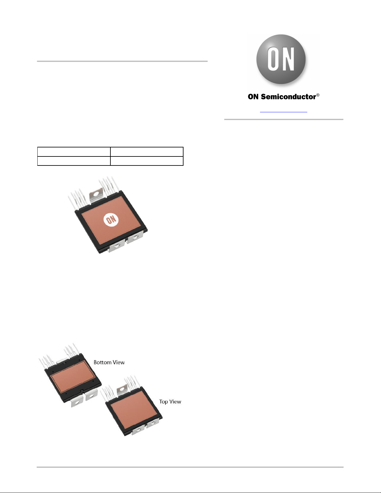
Figure 1.
INTRODUCTION
In order to avoid unnecessary mechanical stress on the
VE−Trac
is important to follow the recommended specifications and
assembly order to install the power module into the end
application power converter. Proper assembly also ensures
good thermal and electrical performance for the power
module assembly.
module, its control leads or the power terminals, it
www.onsemi.com
APPLICATION NOTE
Since the product is only the power module, it should be
noted that this guide will use an example cooler design and
Printed Circuit Board (PCB) to explain the assembly
process. The user has the freedom to design their own
coolers and PCBs to meet their end application
requirements. But the assembly order and certain specific
requirements should be followed.
Recommended mounting order for the assembly:
1. Apply TIM to one side of the power module
2. Align and place power module on 1
cooler
3. Apply TIM to the other side of the power module
4. Align 2
cooler
5. Secure 1
power modules in between
6. Secure PCB to cooler or bracket
7. Solder PCB to power modules
HEATSINK/COOLER REQUIREMENTS
Power dissipated in the module must be effectively
removed from the module without exceeding the maximum
rated operating temperature of the module as specified in its
data sheet. In this section the general requirements for the
cooler is explained and in the following section the assembly
process is explained using an example reference cooler.
nd
half of the cooler to the 1st half of the
st
and 2nd halves of the cooler with the
st
half of the
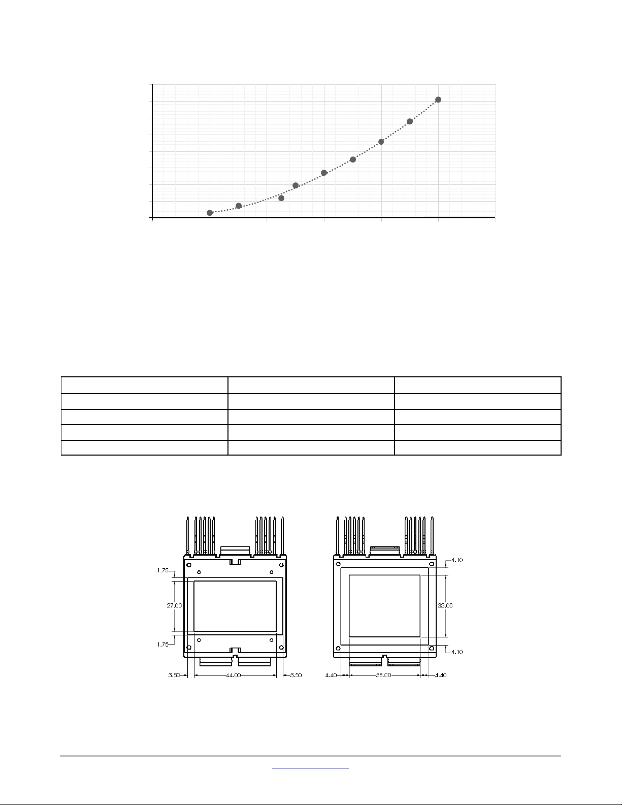
Figure 2. VE−Trac Dual Power Module Showing
the Top and Bottom View
© Semiconductor Components Industries, LLC, 2019
March, 2021 − Rev. 2
General Specifications for the Cooler
• Dual side liquid cooling is necessary to enable the full
capability of the power module.
• It is necessary to use a thermal interface material between
the power module top and bottom area of the Direct Bond
Copper (DBC) to the cooler surface. It’s necessary to
ensure full coverage of the DBCs to the cooler.
• The specified flatness for the module for top and bottom
clamping area (see Figure 3) is specified as Max. Surface
flatness j 50 mm.
• Mating alignment feature must be included on the cooler
(see Figure 4).
1 Publication Order Number:
AND9984/D
Page 2
AND9984
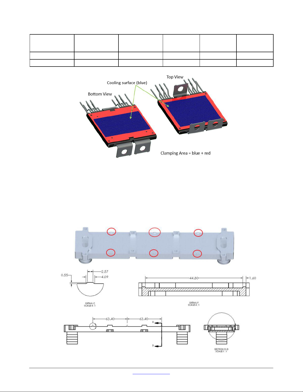
Table 2. SPECIFICATIONS FOR THE COOLER
Max. Cooler
Roughness Rz [mm]
Clamping Area
RED + BLUE AREA 10 50 10 760 7
BLUE AREA 10 50 10 760 5.4
per ISO 4287
Min. Cooler Flatness
[per 100 mm]
per ISO 1101
Max. Step [mm]
per ISO 4287
Minimum
Clamping
Force [N]
Maximum
Clamping
Force [kN]
Figure 3. The Area Shown in Red is Where the Clamping Force Should Be Applied to Ensure Good Contact
In Figure 3 the cross sectional area where the clamping
force should be applied is shown in red and blue. It’s
important not to apply force on the DBC only (blue area),
since it can crack the DBC and damage the module. You can
also get cracked DBC if the specifications of the heatsink
flatness is not met. The blue area shown in Figure 3 is the
The cooler should also include the module alignment
features as shown in Figure 4. This protrusion feature has a
mating feature on the power module to control the module
orientation and spacing between the modules. Figure 4
shows the dimensions and spacing to be included for the
alignment features.
area that should be actively cooled to ensure optimal thermal
performance.
Figure 4. Alignment Feature to Be Included on the Bottom Half of the Cooler
www.onsemi.com
2
Page 3
AND9984
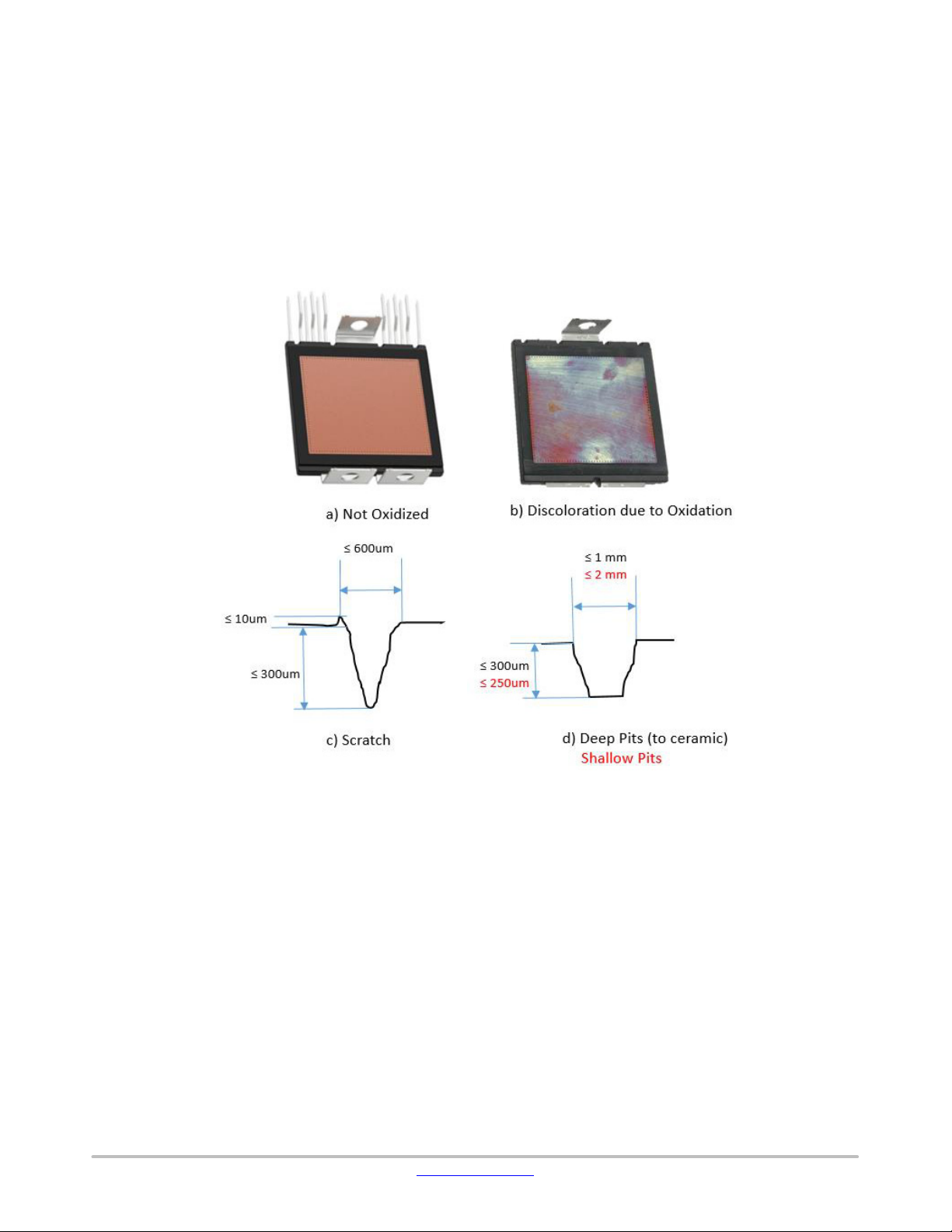
DBC Appearance
The cooling surfaces (DBC) as shown in Figure 3 can
sometimes appear to be discolored, scratched or pitted. The
discoloration is due to the copper on the DBC getting
oxidized due to prolonged exposure to air. The oxide layer
is thin (1.8 – 14 nm) and forms non−uniformly, resulting in
various shades of colors. The contribution of the copper
oxide layer to the thermal performance of the module is so
small that it has no effect on the Rth.j−f (junction to fluid) of
the module.
Other common issues seen on the DBC include scratches
and pitting. This can occur due to handling during assembly
or assembly rework. Figure 5 shows some examples of these
common issues and acceptable criteria for each type. Copper
oxide layer, scratches and pits within the acceptable criteria
have no impact on the electrical, thermal or isolation voltage
capability of the power module.
Figure 5. Different Acceptable Criteria of the Module DBC
Reference Cooler Design and Performance
The reference cooler design can be used as a guide by
customers to develop their own cooler designs. There is no
specific requirement to use this design for the cooler. The
thermal data shown in the data sheet for VE−Trac Dual
products are all measured using this reference cooler. The
www.onsemi.com
cooler can be designed in different ways as long as the
minimum requirements described in the previous section are
met and the proper trade−off consideration is given to the
thermal resistance/impedance, pressure drop and flow rates.
Reference design shown in Figure 6 should be considered as
an example.
3
Page 4
AND9984
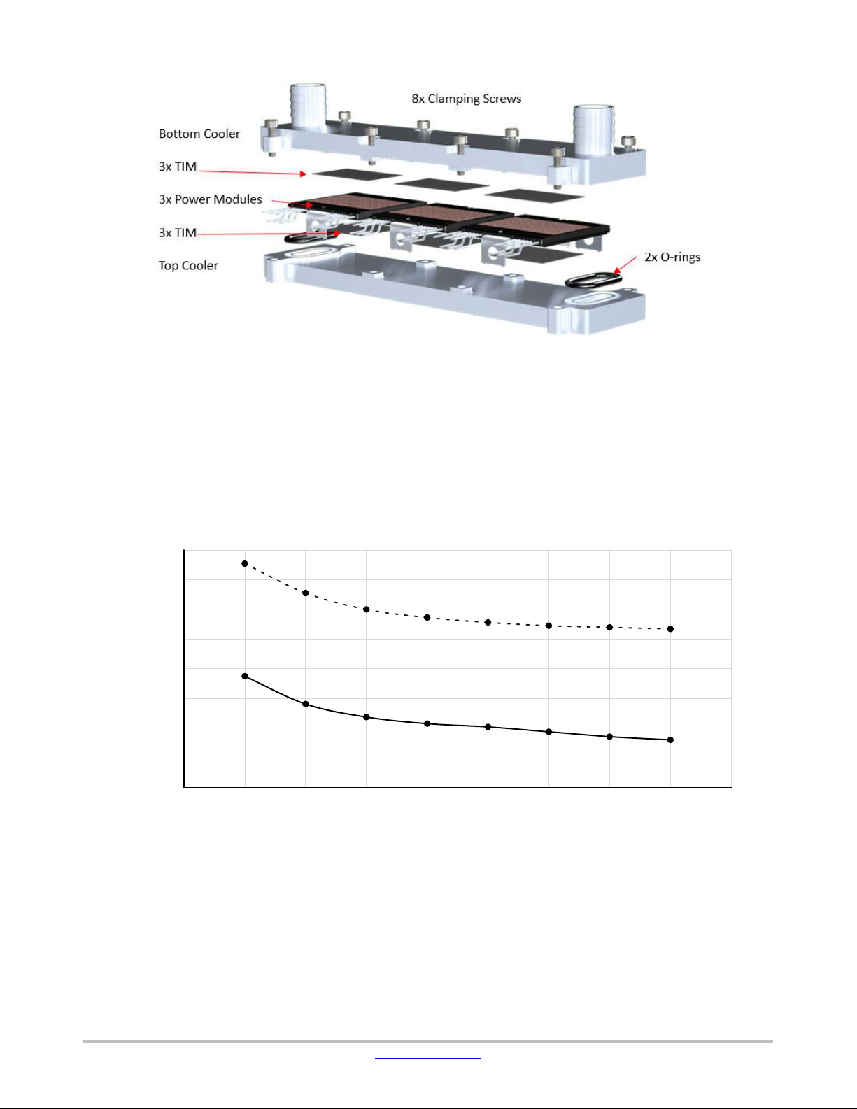
Figure 6. Example Cooler for Use with the VE−Trac Dual
The reference cooler uses a simple pin−fin design and is
optimized for thermal performance, pressure drop and cost.
The data shown below in Figure 7 and Figure 8 should be
considered as typical performance of the cooler with three
750 V, 800 A VE−Trac Dual modules assembled using the
Rth,j−f vs. Flow rate, TF = 655C, 50/50 EGW
0,260
0,240
0,220
0,200
0,180
0,160
Rth,j−f (K/W)
0,140
0,120
0,100
02468101214
recommended thermal interface material and the assembly
process described later in the document. All measurements
were performed using 50/50 Ethylene Water Glycol mix at
65°C as the coolant. The maximum static withstand pressure
of the reference heatsink is 4 Bar.
FWD
IGBT
16 18
Flow Rate (LPM)
Figure 7. Thermal Performance Rth.j−f for IGBT and Diode at Coolant Temperature of 655C
www.onsemi.com
4
Page 5
AND9984
Pressure Drop (mBar) vs. Flowrate (LPM)
80
70
60
50
40
30
20
Pressure Drop (mBar)
10
0
0.0 2.0 4.0 6.0
Flowrate (LPM)
Figure 8. Pressure Drop versus Flow Rate for the Reference Heatsink Coolant @ 655C
8.0 10.0 12.0
Thermal Interface Material (TIM)
Use of an effective Thermal Interface Material is crucial
to achieving the best thermal performance. For VE−Trac
Dual assemblies we recommend using the Honeywell
PTM7000 die cut Phase Change Material at 200 mm
thickness. This material has been tested with the product and
used in all thermal measurements shown on the product data
sheet.
Table 3. CRITICAL PROPERTIES OF THE RECOMMENDED THERMAL INTERFACE MATERIAL (TIM)
Physical Properties
Thermal Conductivity W/m·K 6.5
Thermal Impedance @ No Shim °C.cm2/W 0.06
Specific Gravity g/cm
Volume Resistivity
The PTM7000 is also available in paste form to be used
with automated dispensing machines. Please refer to the
supplier for additional information on its handling and use.
Unit Honeywell PTM7000
3
W·cm
2.7
2.1x10
Figure 9 shows the size and positioning of the die cut
PTM7000 pad placement on the top and bottom cooling
areas of the VE−Trac power modules.
Figure 9. Recommended Size and Location of the TIM Pads for Bottom (left) and Top (right) Side
It is possible to use other TIM materials from other
suppliers in either pad or paste form. However, the new
www.onsemi.com
material will have to be characterized to determine its
performance and optimal method of use in assembly.
5
Page 6

AND9984
REFERENCE COOLER ASSEMBLY
The reference cooler described in the previous section is
used as example to explain the recommended assembly
process of the half−bridge VE−Trac Dual modules into a
STEP 1: Cooler placement in Jig
The bottom side cooler plate in inverter and placed in a jig. We refer to this side of the cooler plate as the bottom half, since it is contact
with bottom side of the power module. The recommended jig design is described below in detail. The purpose of the jig is to securely
hold the bottom half of the cooler plate while the power stack is being assembled.
3−phase power stack i.e. three power modules integrated
with a cooler. The complete assembly process is described
in the following steps:
Figure 10. Jig to Help Assemble the Power Module Stack to the Cooler
www.onsemi.com
6
Page 7

AND9984
STEP 2: TIM Application and Module placement
The TIM pads are aligned and placed as shown in Figure 9 to the bottom side (smaller DBC) of the power modules. The power module
with the TIM is then inverted and placed on the bottom cooler plate in the jig using the alignment features on the module and the cooler
plate to ensure proper orientation and placement.
STEP 3: TIM Application, O−ring and Cooler
The TIM pads are aligned and placed as shown in Figure 9 to the top side (larger DBC) of the power modules. Two O−rings are placed
as shown to seal the coolant flowing between the top and bottom cooler halves. The top cooler half is then visually aligned using the
eight mounting holes and placed on top of the three power modules as shown above.
www.onsemi.com
7
Page 8

The O−ring design for the reference cooler is shown
below in Figure 11:
Figure 11. O−ring Design for the Reference Dual Side Cooler
AND9984
For automotive applications it is typical to use double or
triple edge seal O−rings. In the above example a single edge
seal O−ring is shown as an example for the reference
STEP 4: Securing the Cooler Halves
heatsink. There are other heatsink designs that do not use
O−rings, but is instead welded or braized.
The stack assembly is now inverted bottom side up and secured using the eight screws. Heatsink secured using an ISO 4762 M4 x
0.7 mm Thread X 16 mm long Stainless Steel Socket Head Cap Screw in combination with a DIN 7980 M4 stainless steel split lock
washer. The screws are fastened in the order shown above in a 3 step torque sequence. First torque each screw in order shown to 10%
of the recommended torque value of 1 Nm. Second step is to torque each screw in order to 75% of recommended torque. The complete
assembly is then cured in an oven at 65°C for 30 minutes as recommended by the TIM supplier. Once cured and removed from the
oven, the screws are immediately torqued in order shown to the final recommended torque value of 1 Nm. The process can be different
for different types of TIM and heatsink designs.
www.onsemi.com
8
Page 9

AND9984
POWER TERMINAL CONNECTIONS
There are limited options to connect the module power
terminals to bus bars. The oxygen free copper power
terminals are tin plated and well suited for screw type
fastening.
Terminal Connection Options
The power terminal connections should be made to bus
bars are shown in Figure 12. An isolator with captured nuts
(see Figure 19) is used between the module terminal and
heatsink or chassis. The power module terminals go over the
isolator and the captive nuts and the bus bars over that and
a screw is used to fasten the bus bars to the module terminals.
Hardware shown:
Screw – DIN 439B M6 x 1 mm thread Thin Hex nut
Nut – ISO 7380 M6 x 1 mm thread x 8 mm long
Limitations
The mounting process should result is a system that will
limit the forces acting on the power terminals when secured
to the bus bars. Figure 13 shows the maximum allowed
forces and their axis on the module power terminal.
Figure 13. Force Limitations on the Power Terminal
in All Axis
PRINTED CIRCUIT BOARD (PCB) GUIDELINES
The general recommendation for the plated through holes
for the control pins are shown in Table 4 and Figure 14 shows
the recommended drill hole pattern. Depending on the
design of the PCB there are different methods to solder the
control pins to the PCB. Wave soldering or hand soldering
are the general practice for through−hole type (THT)
components.
Figure 12. Recommended Stack Up for Module
Power Terminal Connections
Figure 14. Recommended Drill−hole Pattern for the PCB
www.onsemi.com
9
Page 10
AND9984
Table 4. SPECIFICATIONS FOR PLATED THROUGH HOLES ON PCB FOR THE SOLDERABLE MODULE CONTROL
PINS
# Description Min. Typ. Max.
1 Initial hole diameter (mm) 1.95 2.00 2.15
2
3
4 Final hole diameter (mm) − 1.85 −
5
6 PCB Thickness (mm) 0.8 1.6 −
Copper thickness in via (mm)
Metallization (Sn) in via (mm)
Annular ring (mm)
25 − −
10 − −
200 − −
Manual Soldering
The recommended conditions for manual soldering are
listed in Table 5. Considering the glass transition
temperature (Tg) of the package mold resin and the thermal
withstand capability of internal chips, the temperature of the
terminal root part should be kept below 150°C. Iron tip
should touch the lead terminal keeping certain distance from
the package mold body. Manual soldering is not
recommended for mass production as it may be difficult to
control the amount of solder applied and the time and
temperature of the soldering step.
Table 5. SPECIFICATIONS FOR MANUAL SOLDERING
CONDITIONS
Single Side Circuit
Parameter
Iron tip
temperature
Soldering time 2 – 6 seconds 4 – 10 seconds
Wave Soldering
Board
385 ± 10°C 420 ± 10°C
Double/Multi−layer
Circuit Board
Assembles are placed on a carrier belt and run the
soldering process to contact the wave solder. The wave
soldering process typically uses a thermal profile which
consists of four stages: solder fluxing, preheating zone,
solder wave and cooling zone. Solder flux is either sprayed
or foamed into the components. Then goes to the preheating
zones, normally by convention, where the flux is activated.
The assembly then goes to wave soldering and slowly cooled
down. Key elements such as preheat ramp rate, conveyor
speed, peak temperature and time forms a wave solder
profile. Wave soldering profile should be optimized in the
assembly site since it strongly depends on the equipment
condition and the material type used in application. A typical
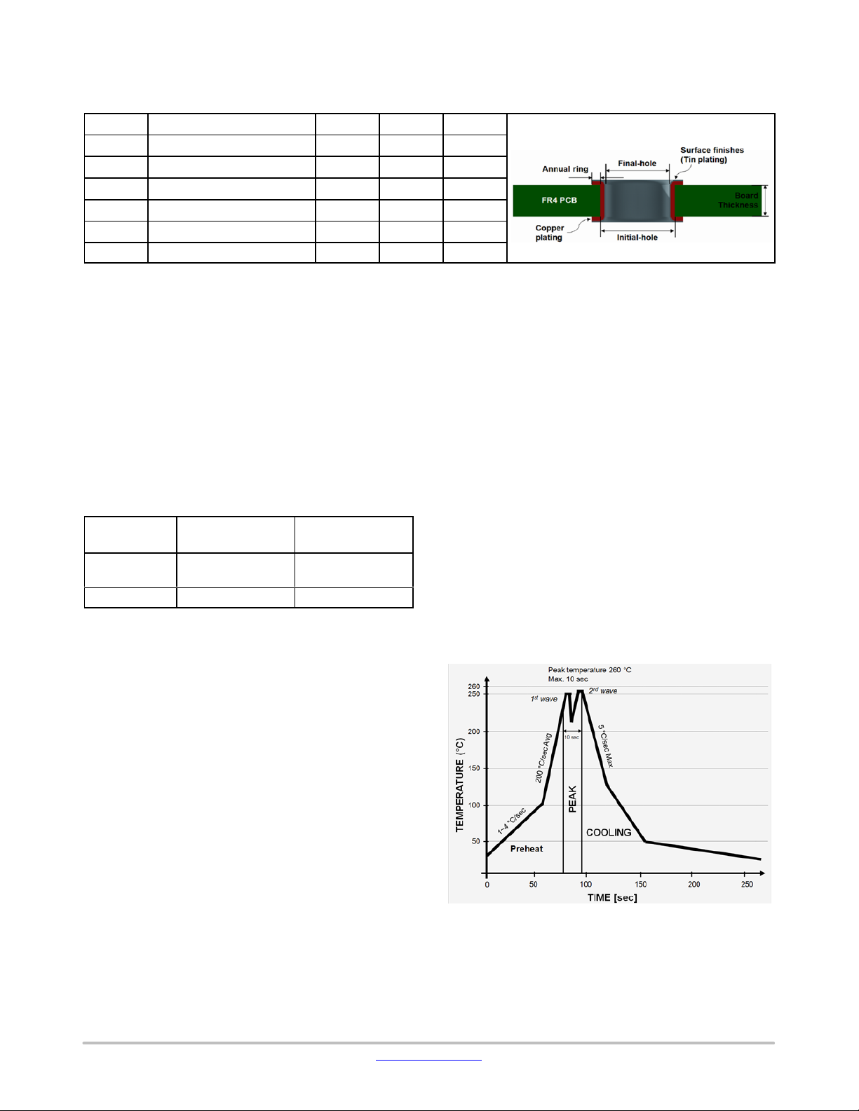
soldering profile and conditions is illustrated in Figure 15
and recommended specifications are shown in Table 6 for
different solder types.
Preheat: Preheat is required to avoid any possible thermal
stress due to overheating. Preheat temperatures and the
preheating time should be set according to the flux
specification. Too high a temperature and too long a duration
may break down the flux activation systems which can cause
unintentional shorts. On the other hand, too low a preheat
temperature setting may cause skips or unwanted residues
left on the PCB. Ramp up rate between 1~4°C per second is
suggested in the preheat zone.
Wave soldering: Dual−wave soldering is the most
common method. The 1st wave which has turbulent wave
crest ensures wetting of all the landing pads, allowing the
molten solder to find its way to all joints on the PCB. The 2nd
wave, which has a laminar flow, drains the excess solder
from the board after the 1st wave thus removing the solder
bridges. It is recommended that maximum soldering
temperature up to 260°C for 10 sec is maintained to establish
a good quality of the solder joint and to avoid package
damage by thermal shock.
Cooling: Gradually cool the processed board down. A
cool down rate between 1 − 5°C/s is recommended in
general.
Figure 15. Typical Dual Solder Profile
www.onsemi.com
10
Page 11

AND9984
Table 6. RECOMMENDED WAVE SOLDERING CONDITIONS
Profile Feature SnPb Eutectic Assembly Pb−Free Assembly
Average ramp up rate ~200°C/sec ~200°C/sec
Preheat ramp up rate Typical 1 − 2, max 4°C/sec Typical 1 − 2, max 4°C/sec
Final preheat temp. ~130°C ~130°C
Peak wave soldering temperature max 235°C, max 10 sec max 260°C, max 10 sec
Ramp down rate 5°C/sec max 5°C/sec max
Solder Inspection
Monitoring the soldering quality is essential, since
abnormal solder joints are potential risks for failures.
IPC−A−610 (DE) standard specifies the soldering quality
criteria for soft soldering. For the examination of a solder
joint, visual or X−ray inspection and automatic optical
inspection are suitable evaluation methods.
Figure 16 shows the recommended final position of a
4−layer PCB (1.6 mm) relative to the edge of the power
module. The minimum recommended space from the edge
of the module to the PCB surface is 10mm spacing. Moving
it closer will likely bend the control pins. Likewise, the
maximum distance between the module edge and PCB
surface should be 18.38 mm. It is generally recommended
that the distance between the PCB and the module edge be
kept as short as possible for optimal performance.
Table 7. CREEPAGE AND CLEARANCE
Parameter Value
Clearance Power Terminal – Power Terminal 3.4 mm
Clearance Power Terminal – Signal Pin 3.1 mm
Clearance Signal Pin – Signal Pin 3.0 mm
Clearance signal pin – Ref. cooler 10.2 mm
Clearance power terminal – ref. cooler 7.0 mm
Creepage Power Terminal – Power Terminal 6.2 mm
Creepage Signal Pin – Signal Pin 5.8 mm
Creepage Power Terminal – Signal Pin 5.9 mm
Creepage Power Terminal – ref. cooler 5.22 mm
Creepage signal pin – ref. cooler 5.22 mm
Table 7 summarizes the creepage and clearance distances
between the various pins of the module and also between the
reference cooler to the different module pins. Figure 17
illustrates the various distances noted in Table 7. Great care
should be taken not to violate the minimum clearance and
creepage requirements when assembling the power module
to heatsinks and using fasteners to secure cables or bus bars
to the module terminals.
Figure 16. PCB Position to Module
SYSTEM ASSEMBLY REQUIREMENTS
The VE−Trac Dual represents a new standard for
packaging power modules for high power applications. It
offers many possibilities for designing more compact power
converters, but there are certain minimum requirements that
must be met to ensure optimal performance.
Creepage and Clearance Requirements
All VE−Trac Dual modules comply with the required
creepage and clearance distances as summarized in the table
below. The module offers basic isolation, pollution degree
2 and a Comparative Tracking Index (CTI) value > 600.
www.onsemi.com
Figure 17. Illustration of Creepage and Clearance
Distances
11
Page 12

AND9984
In order to increase the creepage and clearance between
the cooler and the pins it is necessary to use an isolator. The
and nut has reduced the distance between the high potential
power terminal and the grounded metal cooler.
issue is illustrated in Figure 18. The addition of the screw
Figure 18. Illustration of the Clearance Issue when Using Fasteners to Secure the Power Module Terminals
There are several methods to overcome this clearance
issue depending on your cooler design. However, one of the
methods is discussed as an example. This method captures
the nuts in a floating isolator as shown in the figure below.
integration of the DC link capacitor. The goal is to minimize
the parasitic inductance between the power module and the
bus capacitor. High parasitic inductance will impact the
switching losses of the power modules. Again, there are
multiple options for integrating a DC link and far less critical
is the integration of the output current sensors. Two example
methods are illustrated.
The first example is the Horizontal Integration Concept −
It integrates the DC bus capacitor (from SBE) below the
power stack (power modules + cooler). The DC link uses a
laminated bus structure to connect the power terminals on
the module to the bus capacitor as shown in Figure 20. It uses
a 3−pak, off the shelf hall−effect current sensor from LEM
(HAH3DR 900−S00) with copper AC bus bars. This concept
Figure 19. Using a Floating Isolator with Captured
Nuts is a Potential Solution
positions the gate driver board over the power stack and
cable harness to connect the driver output to a daughter
board that is soldered on to the power module. This design
DC Link, Current Sensor and Gate Driver Integration
Another critical design area that can also impact
primarily meant for evaluation and offers flexibility and
ease in probing signals during evaluations.
performance of the converter system is the mechanical
Figure 20. Horizontal Concept for Integration
The front isometric view of the horizontal concept
(Figure 21) shows how the phase current sensor is integrated
with the power stack. It also shows how the module interface
www.onsemi.com
board is connected to the power module and then a cable is
used to connect the interface board to the driver board on top
of the power module cooler.
12
Page 13

AND9984
Figure 21. Front Isometric View of the Horizontal Integration Concept
The second example is the Vertical Integration Concept
and it is suited for paralleling the VE−Trac Dual modules to
develop high power converters. This concept orients the
power modules vertically and allows the modules to be
stacked in multiples of three to create a compact and scalable
high power inverter. Figure 22 illustrates this concept in
more detail with the parallel integration of 6 (2 modules per
phase) VE−Trac Dual modules. It uses a single large PCB for
driver and controller and the power stack is attached via
screws to the PCB. The large DC bus capacitor from SBE is
located behind the stack with DC link snubber capacitors
attached very close to the paralleled power modules. In this
example concept hall−effect current sensors from LEM
(HAH1DRW 1100−S) are directly attached to the AC bus
bars.
Figure 22. Vertical and Scalable Integration Concept
www.onsemi.com
13
Page 14

AND9984
VISUAL MARKINGS
The product has a number of visual markings to enable
traceability of the materials. It’s important to link the
traceability from the chip to the inverter to maintain an
effective traceability chain.
Figure 23. Traceability Markings on the Power Module
Table 8. EXPLANATION OF MARKINGS
Marker Description
Company Logo ON Semiconductor Logo
2D Code 1 Assembly Lot Number + S/N
2D Code 2 P/N+ Assy. Lot Number + Site & Date
Code + Tool ID + S/N
Site and Date Code Assembly location (XX) and date code
(YWW)
Lot Code Last 3 digits of lot number
S/N Number 7 digit Serial number
P/N Number 7 Character Product part number
Storage and Shipping
Transporting and storing the modules requires care to
avoid extreme shock, vibration and environments. The
Traceability and Identification
Figure 23 and Table 8 together describe all the visual
markings on the module and provide an explanation of the
markers.
recommended storage conditions for the module according
to IEC 60721−3−1, class 1K2 should be followed and
storage time should not exceed two years from
manufactured date code. Below is a summary of the
recommended storage parameters:
Table 9. STORAGE SPECIFICATIONS
Parameter Value Unit
Maximum air temperature 40 °C
Minimum air temperature +5 °C
Maximum relative humidity 85 %
Minimum relative humidity 5 %
Condensation Not Allowed
Precipitation Not Allowed
Icing Not Allowed
VE−Trac is trademark of Semiconductor Components Industries, LLC (SCILLC) or its subsidiaries in the United States and/or other countries.
ON Semiconductor and are trademarks of Semiconductor Components Industries, LLC dba ON Semiconductor or its subsidiaries in the United States and/or other countries.
ON Semiconductor owns the rights to a number of patents, trademarks, copyrights, trade secrets, and other intellectual property. A listing of ON Semiconductor’s product/patent
coverage may be accessed at www.onsemi.com/site/pdf/Patent−Marking.pdf. ON Semiconductor reserves the right to make changes without further notice to any products herein.
ON Semiconductor makes no warranty, representation or guarantee regarding the suitability of its products for any particular purpose, nor does ON Semiconductor assume any liability
arising out of the application or use of any product or circuit, and specifically disclaims any and all liability, including without limitation special, consequential or incidental damages.
Buyer is responsible for its products and applications using ON Semiconductor products, including compliance with all laws, regulations and safety requirements or standards,
regardless of any support or applications information provided by ON Semiconductor. “Typical” parameters which may be provided in ON Semiconductor data sheets and/or
specifications can and do vary in different applications and actual performance may vary over time. All operating parameters, including “Typicals” must be validated for each customer
application by customer’s technical experts. ON Semiconductor does not convey any license under its patent rights nor the rights of others. ON Semiconductor products are not
designed, intended, or authorized for use as a critical component in life support systems or any FDA Class 3 medical devices or medical devices with a same or similar classification
in a foreign jurisdiction or any devices intended for implantation in the human body. Should Buyer purchase or use ON Semiconductor products for any such unintended or unauthorized
application, Buyer shall indemnify and hold ON Semiconductor and its officers, employees, subsidiaries, affiliates, and distributors harmless against all claims, costs, damages, and
expenses, and reasonable attorney fees arising out of, directly or indirectly, any claim of personal injury or death associated with such unintended or unauthorized use, even if such
claim alleges that ON Semiconductor was negligent regarding the design or manufacture of the part. ON Semiconductor is an Equal Opportunity/Affirmative Action Employer. This
literature is subject to all applicable copyright laws and is not for resale in any manner.
PUBLICATION ORDERING INFORMATION
LITERATURE FULFILLMENT:
Email Requests to: orderlit@onsemi.com
ON Semiconductor Website: www.onsemi.com
◊
TECHNICAL SUPPORT
North American Technical Support:
Voice Mail: 1 800−282−9855 Toll Free USA/Canada
Phone: 011 421 33 790 2910
www.onsemi.com
Europe, Middle East and Africa Technical Support:
Phone: 00421 33 790 2910
For additional information, please contact your local Sales Representative
14
 Loading...