

Page 1
AND9954/D
Multi-Core Configuration of
LC823455 Series for Audio
Applications
Introduction
This application note describes multi−core configuration
for the implementation of multi−core RTOS (Real Time
Operating System).
First, the H/W requirements for the implementation of
multi−core RTOS are described, and then the S/W
requirements are described.
The intended audience is customers who are developing
audio applications using LC823455 Series (called
LC823455 hereafter).
BACKGROUND
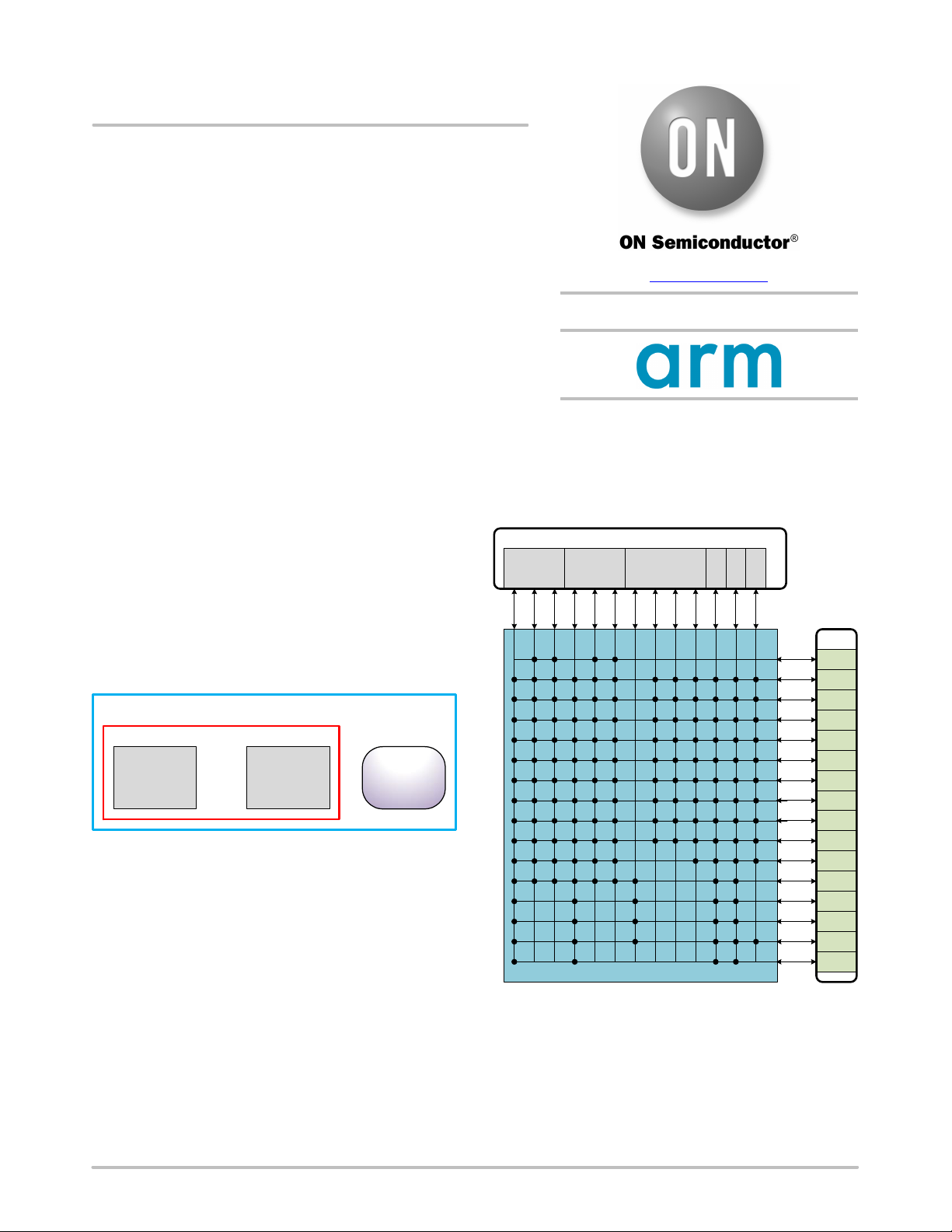
Implemented Cores
LC823455 has two Arm® Cortex−M3 processors (Core0
and Core1) and one proprietary−DSP called LPDSP. LPDSP
is used for audio processing, and its instruction set is
different that of Cortex−M3 processor. Therefore, in
LC823455 the two Cortex−M3 processors and the LPDSP
are configured to heterogeneous multi−core architecture as
outlined with the blue frame in Figure 1. On the other hand,
as focus on the two Cortex−M3 processors they are
configured to homogeneous dual−core architecture as
outlined with the red frame in Figure 1.
Heterogeneous Multi-core Configuration
Homogeneous Dual-core Configuration
Arm Cortex -M3
(Core0)
Arm Cortex -M3
(Core1)
LPDSP
Figure 1. Core Configuration of LC823455
HARDWARE REQUIREMENTS
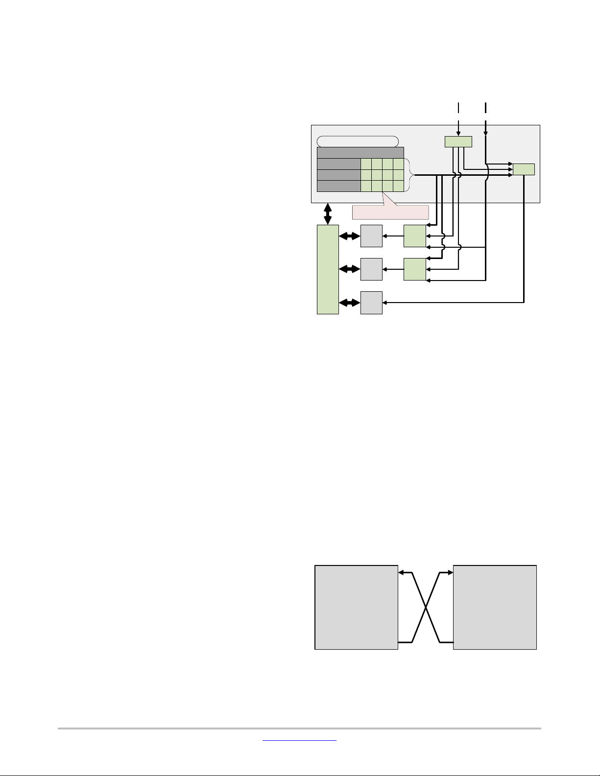
Memory Access from Cores
LC823455 has multiple bus masters including the two
Cortex−M3 processors, and multiple bus slaves as described
in Figure 2. The bus masters access the bus slaves via a bus
matrix depicted by • in Figure 2.
Cortex−M3 processors (core0 and core1) can access all
bus slaves except the LPDSP32−ROM. Access latency to
a target bus slave from both cores of Cortex−M3 processors
is the same if they both don’t access to same bus−slave at the
same time. If they both try to access the same slave at the
same time, one core will have to stall while the other one
completes its access first.
www.onsemi.com
APPLICATION NOTE
Multiple bus masters can access different bus slaves at the
same time via the bus matrix. When multiple bus masters
access to same bus slave at the same time, bus matrix
performs bus arbitration.
Master
Arm Cortex -M3
(Core0)
System-BUS
Bus-Matrix
Arm Cortex -M3
(Core1)
System-BUS
D-BUS
I-BUS
I-BUS
LPDSP
D-BUS
DMIO
DMA
DMB
DMAC0USB
DMAC0
PM
DMA
2.0
C1
DMAC1
DMAC
Slave
System
ROM
SEG0
SEG1
SEG2
SEG3
SEG4
SEG5
SEG6
SEG7
SEG8
SEG9
BASIC
EXT1
EXT3
EXT4
APB
Figure 2. Bus−matrix of LC823455
Note about bus arbitration:
• PM, DMA and DMB access from LPDSP are top priority
and always preferred.
• Access from master except LPDSP is usually scheduled
in round−robin arbitration.
© Semiconductor Components Industries, LLC, 2019
May, 2020 − Rev. 2
1 Publication Order Number:
AND9954/D
Page 2
AND9954/D
Mutex
Mutual exclusion (Mutex) is used to enable exclusive
access control to critical bus slaves. Using Mutex, it is
possible to maintain the consistency of data. LC823455 has
16 mutex registers.
Atomic Instruction
Cortex−M3 supports bit−band instruction. This
instruction performs an atomic read−modify−write
operation with exclusive access to memory. Using this
instruction, it is possible to maintain the consistency of data.
LPDSP doesn’t support atomic instruction.
Unique id
Cortex−M3 processors (both core0 and core1) have
unique CPUID in address 0xE00F_E000 respectively. Since
this address is accessed through the Private Peripheral Bus
(PPB), each core can access a unique register.
CPUID for Cortex−M3 core0 indicates 0 (“0” is allocated
in 0xE00F_E000 for Cortex−M3 core0).
CPUID for Cortex−M3 core1 indicates 1 (“1” is allocated
in 0xE00F_E000 for Cortex−M3 core1).
When unique program codes for each core are included in
one as a common program code, each core recognize its
CPUID on boot, and then executes its respective unique
program code.
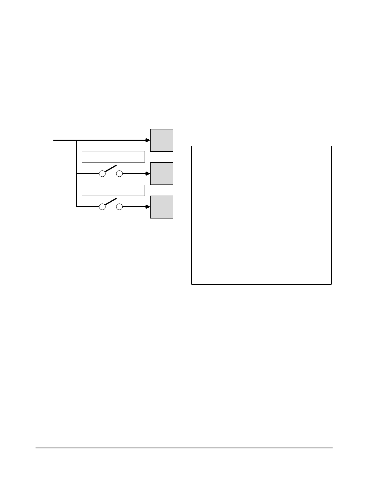
Interrupts between Cores
LC823455 has 12 interrupts be generated between the
cores as shown in Figure 3. Interrupts to Cortex−M3 (core0
and core1) are connected via the NVIC. Interrupts to LPDSP
are connected via the SELECTOR.
INTISR0_0, INTISR0_1, INTISR0_2 and INTISR0_3
are used to generate interrupts from Cortex−M3 core0.
When Cortex−M3 core0 sets a value of “1” on INTISR0_0,
an interrupt is generated from Cortex−M3 core0 to
Cortex−M3 core0, core1 and LPDSP. NTISR0_1,
INTISR0_2, and INTISR0_3 operate in the same way as
INTISR0_0.
INTISR1_0, INTISR1_1, INTISR1_2 and INTISR1_3
are used to generate interrupts from Cortex−M3 core1.
When Cortex−M3 core1 sets a value of “1” on INTISR1_0,
an interrupt is generated from Cortex−M3 core1 to
Cortex−M3 core0, core1 and LPDSP. NTISR1_1,
INTISR1_2 and INTISR1_3 operate in the same way as
INTISR1_0.
INTISR2_0, INTISR2_1, INTISR2_2 and INTISR2_3
are used to generate interrupts from LPDSP. When LPDSP
sets a value of “1” on INTISR2_0, an interrupt is generated
from LPDSP to Cortex−M3 core0, core1 and LPDSP.
NTISR2_1, INTISR2_2 and INTISR2_3 operate in the
same way as INTISR2_0.
External interrupts refer to interrupts from the GPIOs.
And Functional interrupts refer to interrupts from function
blocks. External interrupts are provided via the FILTER to
remove a noise.
External
Functional
Interrupt
Interrupt
Register name: IPIREG
Address: 0x4000_3000
Invalid(Bit31−24)
Invalid(Bit23−20)
Invalid(Bit15−12)
Invalid(Bit7−4)
These12bits registers are cleared by registers below.
Register name: IPICLR( Address:0x4000_30004)
BUS−MATRIX
INTISR2
INTISR2
_3
(Bit19)
(Bit18)
INTISR1
INTISR1
_3
(Bit11)
(Bit10)
INTISR0
INTISR0
_3
(Bit3)
Arm
Cortex−M3
(Core0)
Arm
Cortex−M3
(Core1)
LPDSP
INTISR2
_2
_1
(Bit17)
INTISR1
_2
_1
(Bit9)
INTISR0
_2
_1
(Bit2)
(Bit1)
INTCNT
FILTER
etc
INTISR2
_0
(Bit16)
INTISR1
_0
(Bit8)
INTISR0
INTISR0
_0
_0
(Bit0)
(Bit0)
NVIC0
NVIC1
SELECTOR
Figure 3. Interrupt of LC823455
Event Communication between Cortex−M3 Core0 and
Cortex−M3 Core1
Figure 4 shows how events are communicated between
Cortex−M3 core0 and Cortex−M3 core1. The TXEV output
of Cortex−M3 Core0 is connected to the RXEV input of
Cortex−M3 Core1. The TXEV output of Core1 is connected
to the RXEV input of Core0.
Both cores can synchronize their tasks by entering into
sleep state via the WFE instruction, and by issuing an event
to exit sleep state via the SEV command.
The behavior of the WFE instruction is affected by an
event latch in the core. If the event latch is not set, the core
will enter into sleep state by the WFE instruction. If the event
latch is set, the latch is cleared and execution of the WFE
instruction does not cause the core to enter sleep state, rather,
it continues normal operation. Please refer to Arm
documentation on the Cortex−M3 WFE command for more
information about the event latch.
RXEV
Arm Cortex−M3
(Core 0)
TXEV
RXEV
Arm Cortex−M3
(Core 1)
TXEV
Interrupt from Peripherals
External interrupts and Functional interrupts are provided
to Cortex−M3 (core0 and core1) and LPDSP as shown in
Figure 3.
www.onsemi.com
Figure 4. Cortex−M3 Multi−Core of Event
Communication
2
Page 3
AND9954/D
Clock and Reset
A Common clock is provided to Cortex−M3 core0, core1
and LPDSP as shown in Figure 5.
The clock for Cortex−M3 core1 is controlled by register
C1CLKEN (0x4008_0000 bit0).
The clock for LPDSP is controlled by register
DSPCLKEN (0x4008_0000 bit8).
Additionally, the reset for Cortex−M3 core1 is controlled
by register C1RSTN (0x4008_0000 bit1) and the reset for
the LPDSP is controlled by register DSPRSTN
(0x4008_0000 bit9).
On boot, the clocks for Cortex−M3 core1 and LPDSP are
stopped and Cortex−M3 core1 and LPDSP are reset.
Arm
Clock
SYSCON
0x4008_0000bit0 C1CLKEN
SYSCON
0x4008_0000bit8 DSPCLKEN
Cortex−M3
(Core0)
Arm
Cortex−M3
(Core1)
LPDSP
Figure 5. Clock Tree of LC823455
SOFTWARE REQUIREMENTS
OS
ON Semiconductor can provide the OS as binary code in
a kernel called TOPPERS/FMP. It conforms to uITRON4
standard profile designed as the operating system for
embedded system and supports multi−core system.
ON Semiconductor can also provide the development
environment including source code, under NDA. Of course,
it is allowed to use other OS which customers have a right
to use as well.
Task Assignment Example for TOPPERS/FMP
When a task is added, the task assignment must be
specified using CRE_TSK in the configuration file, as
shown in Figure 6.
• taskA written in CLASS(TCL_1) is assigned to
Cortex−M3 Core0 initially. But it is possible to assign to
Cortex−M3 Core1 later.
• taskB written in CLASS(TCL_2) is assigned to
Cortex−M3 Core1 initially. But it is possible to assign to
Cortex−M3 Core0 later.
• taskC written in CLASS(TCL_1_ONLY) is assigned to
Cortex−M3 Core0. It cannot be assigned to Cortex−M3
Core1.
• taskD written in CLASS(TCL_2_ONLY) is assigned to
Cortex−M3 Core1. It cannot be assigned to Cortex−M3
Core0.
Task processing also should be written as shown in
Figure 7. The use of ext_tsk () is optional.
For details regarding the arguments for CRE_TSK, please
refer to the TOPPERS/FMP Kernel API Specification.pdf in
LC823455 Sample Software Package.
This is a configuration file example.
CLASS(TCL_1){
//create taskA
CRE_TSK(NEW_TSKA, { TA_ACT, 0, taskA, 1, 1024, NULL });
//define interrupt0
DEF_INH(INHNO_I0, { TA_NULL, interrupt0 });
//set interrupt0 attribute
CFG_INT(INTNO_I0, { LOWLEVEL_DETECT, INTPRIORITY });
}
CLASS(TCL_2){
//create taskB
CRE_TSK(NEW_TSKB, { TA_ACT, 0, taskB, 2, 1024, NULL });
}
CLASS(TCL_1_ONLY){
//create taskC
CRE_TSK(NEW_TSKC, { TA_ACT, 0, taskC, 3, 1024, NULL });
}
CLASS(TCL_2_ONLY){
//create taskD
CRE_TSK(NEW_TSKD, { TA_ACT, 0, taskD, 4, 1024, NULL });
}
Figure 6. Configuration File Example
TOPPERS/FMP
When an interrupt handler is added, it should be defined
using DEF_INH and its attributes set using CFG_INT in the
configuration file as shown in Figure 6. The interrupt
handler processing should be written as shown in the
Figure 6.
For details about the arguments for DEF_INH and
CFG_INT, please refer to the TOPPERS/FMP Kernel API
Specification.pdf in LC823455 Sample Software Package.
www.onsemi.com
3
Page 4

This is C source file example.
Void taskA( intptr_t exinf ){
//process
***********************
ext_tsk();
}
Void taskB( intptr_t exinf ){
//process
***********************
ext_tsk();
}
Void taskC( intptr_t exinf ){
//process
***********************
ext_tsk();
}
Void taskD( intptr_t exinf ){
//process
***********************
}
Void Interrupt0(void){
//process
***********************
}
AND9954/D
Figure 7. C Source Code Example
Arm, Cortex and the Arm logo are registered trademarks of Arm Limited (or its subsidiaries) in the US and/or elsewhere.
ON Semiconductor and are trademarks of Semiconductor Components Industries, LLC dba ON Semiconductor or its subsidiaries in the United States and/or other countries.
ON Semiconductor owns the rights to a number of patents, trademarks, copyrights, trade secrets, and other intellectual property. A listing of ON Semiconductor’s product/patent
coverage may be accessed at www.onsemi.com/site/pdf/Patent−Marking.pdf. ON Semiconductor reserves the right to make changes without further notice to any products herein.
ON Semiconductor makes no warranty, representation or guarantee regarding the suitability of its products for any particular purpose, nor does ON Semiconductor assume any liability
arising out of the application or use of any product or circuit, and specifically disclaims any and all liability, including without limitation special, consequential or incidental damages.
Buyer is responsible for its products and applications using ON Semiconductor products, including compliance with all laws, regulations and safety requirements or standards,
regardless of any support or applications information provided by ON Semiconductor. “Typical” parameters which may be provided in ON Semiconductor data sheets and/or
specifications can and do vary in different applications and actual performance may vary over time. All operating parameters, including “Typicals” must be validated for each customer
application by customer’s technical experts. ON Semiconductor does not convey any license under its patent rights nor the rights of others. ON Semiconductor products are not
designed, intended, or authorized for use as a critical component in life support systems or any FDA Class 3 medical devices or medical devices with a same or similar classification
in a foreign jurisdiction or any devices intended for implantation in the human body. Should Buyer purchase or use ON Semiconductor products for any such unintended or unauthorized
application, Buyer shall indemnify and hold ON Semiconductor and its officers, employees, subsidiaries, affiliates, and distributors harmless against all claims, costs, damages, and
expenses, and reasonable attorney fees arising out of, directly or indirectly, any claim of personal injury or death associated with such unintended or unauthorized use, even if such
claim alleges that ON Semiconductor was negligent regarding the design or manufacture of the part. ON Semiconductor is an Equal Opportunity/Affirmative Action Employer. This
literature is subject to all applicable copyright laws and is not for resale in any manner.
PUBLICATION ORDERING INFORMATION
LITERATURE FULFILLMENT:
Email Requests to: orderlit@onsemi.com
ON Semiconductor Website: www.onsemi.com
◊
TECHNICAL SUPPORT
North American Technical Support:
Voice Mail: 1 800−282−9855 Toll Free USA/Canada
Phone: 011 421 33 790 2910
www.onsemi.com
4
Europe, Middle East and Africa Technical Support:
Phone: 00421 33 790 2910
For additional information, please contact your local Sales Representative
 Loading...