

Page 1
AND9902/D
Digital IF
Encoder
AX5045 Programming
Manual
Ultra-Low Power Narrow-Band Sub GHz
(60−1050 MHz) RF Transceiver with
Integrated +23 dBm High Power Amplifier
www.onsemi.com
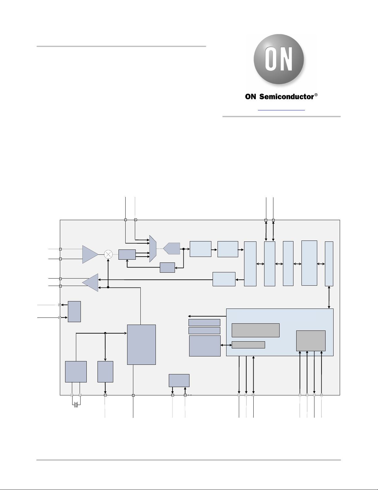
OVERVIEW
AX5045 is a true single chip low-power CMOS
transceiver for narrow band applications. A fully integrated
VCO support most carrier frequencies from 60 MHz to
1050 MHz. The on-chip transceiver consists of a fully
integrated RF front-end with modulator, and demodulator.
Base band data processing is implemented in an advanced
and flexible communication controller that enables user
friendly communication via the SPI interface.
GPADC1
GPADC2
25
26
AX5045
5
VCHOKE
VDD_IO
RX_P
RX_N
TX_P
TX_N
6
3
4
27
1,23
Voltage
Crystal
Oscillator
typ.
16 MHz
28
Regulator
27
LNA
Mixer
IF Filter &
AGC PGAs
PA
OUT
F
XTAL
F
Divider
13
RF Frequency
Generation
Subsystem
RF Output
60 MHz –
1.05 GHz
8
ADC
AGC
Voltage
Regulator
7
APPLICATION NOTE
An on-chip low power oscillator as well as Wake-on-radio
enable very low power standby applications. Figure 1 shows
the block diagram of the AX5045.
DCLK
DATA
12
11
channel
filter
Chip configuration
POR
References
Low Power
Oscillator
640 Hz/10kHz
23,1
De-
modulator
Modulator
Correction
Forward Error
Communication Controller &
Registers
Wake on Radio
19
Serial Interface
Framing
handling
Radio Controller
Radio Controller
timing and packet
timing and packet
SPI
14
FIFO
17
CLKP
CLKN
SYSCLK
© Semiconductor Components Industries, LLC, 2019
March, 2021 − Rev. 1
FILT
VDD_IO
VDD_ANA
IRQ20PWRAMP21ANTSEL
Figure 1. Functional Block Diagram of the AX5045
1 Publication Order Number:
SEL15CLK16MISO
AND9902/D
MOSI
Page 2

AND9902/D
Table of Contents
Overview 1...............................................................................................
FIFO Operation 7.........................................................................................
Programming the Chip 12..................................................................................
Register Overview 21......................................................................................
Register Details 33........................................................................................
References 82............................................................................................
www.onsemi.com
2
Page 3
AND9902/D
AX5045
SEL
AX8052F100
or
other mC
28 27 26 25 24 23 22
1
2
3
4
5
6
7
21
20
19
18
17
16
15
8 9 10 11 12 13 14
RESET_N
PB7/DBG_CLK
DBG_EN
PB6/DBG_DATA
PB5/U0RX/T1OUT
PB4/U0TX/T1CLK
PB3/OC0/T2CLK/EXTIRQ1/DSWAKE
RIRQ/PR5
VDD_CORE
RMOSI/PR4
RMISO/PR3
RCLK/PR2
RSEL/PR0
RSYSCLK/PR1
OMPO0/U0RX/SMISO/PC3
U 0T X/S MO SI/P C2
OMPO1/T0CLK/SSCK/PC1
XTIRQ0/T0OUT/SSEL/PC0
EXTIRQ0/IC1/U1TX/PB0
OC1/U1RX/PB1
T2OUT/IC0/PB2
PA5/ADC5/IC0/U1TX/COMPI10
PA4/ADC4/T1CLK/COMPO0/LPXTA
PA3 /AD C3/T 1OU T/LPX TALP
PA 2/A DC 2 /OC 0/U 1R X/C OM PI0 0
PA1/ADC1/T0CLK/OC1/XTALP
PA 0/A DC 0/T 0 OU T/IC 1/X TAL N
VDD_IO
IRQ
MOSI
MISO
CLK
SYSCLK
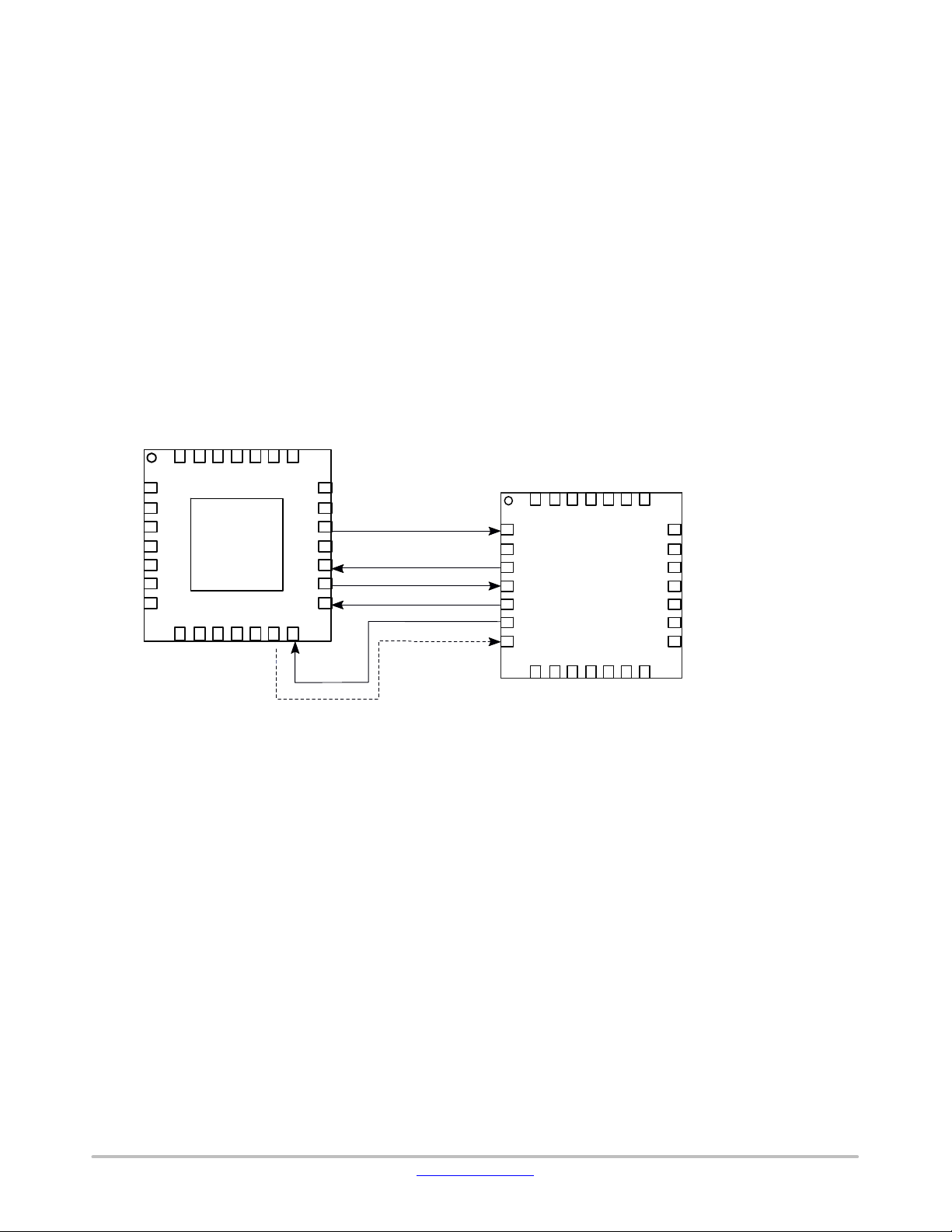
Connecting the AX5045 to an AX8052F100 or other
Microcontroller
The AX5045 can easily be connected to an AX8052F100
or any other microcontroller. The microcontroller
communicates with the AX5045 via a register file that is
implemented in the AX5045 and that can be accessed
serially via an industry standard Serial Peripheral Interface
(SPI) protocol.
Reset is performed by the integrated power-on-reset
(POR) block and can be performed manually via the register
file.
The AX5045 sends and receives data via the SPI port in
frames. This standard operation mode is called frame mode.
NC
NC
VDD_IO
21
ANTSEL
20
PWRAMP
IRQ
19
NC
18
MOSI
17
MISO
16
CLK
15
VDD_IO
VCHOKE
TX_P
TX_N
RX_P
RX_N
VDD_ANA
GPADC2
CLKP
CLKN
28 27 26 25 24 23 22
1
2
3
4
5
6
7
GND
center pad
GPADC1
In frame mode, the internal communication controller
performs frame delimiting, and data is received and
transmitted via a 256 Byte FIFO, accessible via the register
file. The FIFO is shared between receive and transmit.
Figure 2 shows the corresponding diagram. Connecting the
interrupt line is highly recommended, though not strictly
required. It is also recommended to connect the SYSCLK
line, which can be programmed to provide a copy of the
precise crystal clock of the AX5045. Once set up, the
Microcontroller can directly run on that clock or use it to
calibrate its internal oscillators.
810111213149
FILT
NC
NC
SEL
DCLK
DATA
SYSCLK
Figure 2. Connecting AX5045 to AX8052F100 or other mC
www.onsemi.com
3
Page 4

Pin Function Descriptions
Table 1. PIN FUNCTION DESCRIPTION
Symbol
Pin(s)
Type
Description
VDD_IO1P
Power supply 3.0 V – 3.6 V
VCHOKE2P
Regulator Output to External PA choke inductors
TX_P3A
Differential TX antenna output
TX_N4A
Differential TX antenna output
RX_P5A
Differential RX antenna input
RX_N6P
Differential RX antenna input
VDD_ANA
7
P
Analog power output, decoupling
FILT8A
Optional synthesizer filter
NC9A
Not used
NC10A
Not used
DATA11I/O
In wire mode: Data input/output
DCLK12I/O
In wire mode: Clock output
SYSCLK
13
I/O
Default functionality: Crystal oscillator (or divided) clock output Can be pro-
SEL14I
Serial peripheral interface select
CLK15I
Serial peripheral interface clock
MISO16O
Serial peripheral interface data output
MOSI17I
Serial peripheral interface data input
NC18N
Must be left unconnected
IRQ19I/O
Default functionality: Transmit and receive interrupt
PWRAMP
20
I/O
Default functionality: Power amplifier control output
ANTSEL
21
I/O
Default functionality: Diversity antenna selection output
NC22N
Must be left unconnected
VDD_IO23P
Power supply 3.0 V – 3.6 V
NC24N
Must be left unconnected
GPADC125A
GPADC input, must be connected to GND if not used
GPADC226A
GPADC input, must be connected to GND if not used
CLKN27A
Crystal oscillator input/output. Leave unconnected when using TCXO
CLKP28A
Crystal oscillator input/output. TCXO input.
GND
Center pad
P
Ground on center pad of QFN, must be connected
AND9902/D
Can be programmed to be used as a general purpose I/O pin Selectable
internal 65 kW pull−up resistor
Can be programmed to be used as a general purpose I/O pin Selectable
internal 65 kW pull−up resistor
grammed to be used as a general purpose I/O pin Selectable internal 65 kW
pull−up resistor
Can be programmed to be used as a general purpose I/O pin Selectable
internal 65 kW pull−up resistor
Can be programmed to be used as a general purpose I/O pin Selectable
internal 65 kW pull−up resistor
Can be programmed to be used as a general purpose I/O pin Selectable
internal 65 kW pull−up resistor
NOTE: All digital inputs are Schmitt trigger inputs, digital input and output levels are LVCMOS/LVTTL compatible and 5 V tolerant.
A = analog input
I = digital input signal
O = digital output signal
I/O = digital input/output signal
N = not to be connected
P = power or ground
www.onsemi.com
4
Page 5
AND9902/D
Table 2. SPI STATUS BITS
SPI Bit Cell
Status
Register Bit
0
−
1 (when transitioning out of deep sleep, this bit transitions from 0→1 when the power becomes ready)
1
S14
PLL LOCK
2
S13
FIFO OVER
3
S12
FIFO UNDER
4
S11
THRESHOLD FREE ( FIFO Free > FIFO threshold)
5
S10
THRESHOLD COUNT (FIFO count > FIFO threshold)
6
S9
FIFO FULL
7
S8
FIFO EMPTY
8
S7
PWRGOOD (not BROWNOUT)
9
S6
PWR INTERRUPT PENDING
10
S5
RADIO EVENT PENDING
11
S4
XTAL OSCILLATOR RUNNING
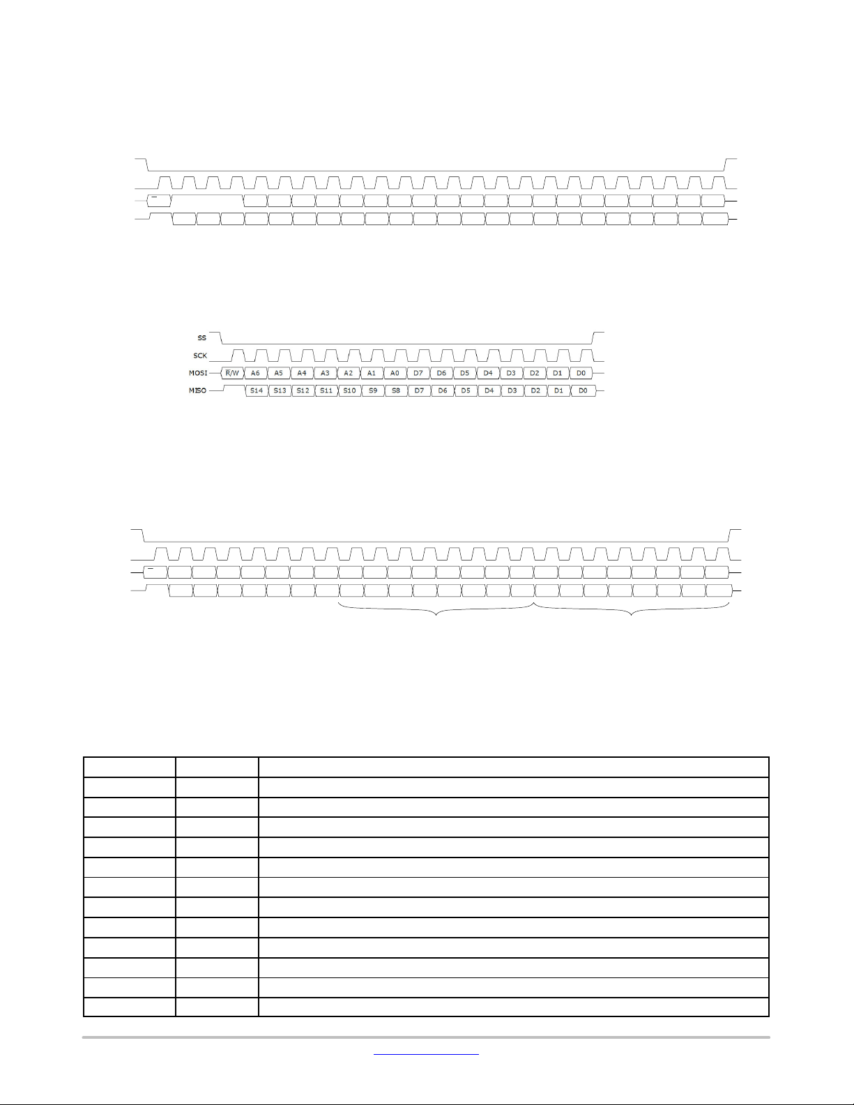
SPI Register Access
Registers are accessed via a synchronous Serial Peripheral
Interface (SPI). Most Registers are 8 bits wide and accessed
using the waveforms as detailed in Figure 3. These
SS
SCK
R/W A7S7A6 A5 A4 A3 A2 A1
MOSI
MISO
S14 S13 S12 S11 S9A8S8
A11 A10 A9
111
S6 S5 S4 S3 S2 S1A0S0
Figure 3. SPI 8bit Long Address Read/Write Access
The most important registers are at the beginning of the
address space, i.e. at addresses less than 0x70. These
Figure 4. SPI 8bit Read/Write Access
Some registers are longer than 8 bits. These registers can
be accessed more quickly than by reading and writing
individual 8 bit parts. This is illustrated in Figure 5. Accesses
are not limited by 16 bits either, reading and writing data
waveforms are compatible to most hardware SPI master
controllers, and can easily be generated in software. MISO
changes on the falling edge of CLK, while MOSI is latched
on the rising edge of CLK.
D7 D6 D5 D4 D3 D2 D1 D0
D7 D6 D5 D4 D3 D2 D1 D0S10
registers can be accessed more efficiently using the short
address form, which is detailed in Figure 4.
bytes can be continued as long as desired. After each byte,
the address counter is incremented by one. Also, this access
form also works with long addresses.
SS
SCK
R/W A6 A5 A4 A3 A2 A1 A0
MOSI
MISO
S14 S13 S12 S11 S10 S9 S8
D7 D6 D5 D4 D3 D2 D1 D0
D7 D6 D5 D4 D3 D2 D1 D0
Figure 5. SPI 16bit Read/Write Access
During the address phase of the access, the chip outputs
the most important status bits. This feature is designed to
speed up software decision on what to do in an interrupt
D7 D6 D5 D4 D3 D2 D1 D0
D7 D6 D5 D4 D3 D2 D1 D0
A A+1
handler. The table below shows which register bit is
transmitted during the status timeslots.
www.onsemi.com
5
Page 6

Table 2. SPI STATUS BITS (continued)
12
S3
WAKEUP INTERRUPT PENDING
13
S2
LPOSC INTERRUPT PENDING
14
S1
GPADC INTERRUPT PENDING
15
S0
undefined
SPI Bit Cell Register BitStatus
AND9902/D
Note that bit cells 8−15 (S7…S0) are only available in two
address byte SPI access formats.
Deep Sleep
The chip can be programmed into deep sleep mode. In
deep sleep mode, the chip is completely switched off, which
results in very low leakage power. All registers loose their
programming.
To enter deep sleep mode, write the deep sleep encoding
into bits 3:0 of PWRMODE. At the rising edge of the SEL
line, the chip will enter deep sleep mode.
To exit deep sleep mode, lower the SEL line. This will
initiate startup and reset of the chip. Then poll the MISO
line. The MISO line will be held low during initialization,
and will rise to high at the end of the initialization, when the
chip becomes ready for further operation.
Address Space
The address space has been allocated as follows.
Addresses from 0x000 to 0x06F are reserved for “dynamic
registers”, i.e. registers that are expected to be frequently
accessed during normal operation, as they can be efficiently
accessed using single address byte SPI accesses. Addresses
from 0x070 to 0x0FF have been left unused (they could only
be accessed using the two address byte SPI format).
Addresses from 0x100 to 0x1FF have been reserved for
physical layer parameter registers, for example receiver,
transmitter, PLL, crystal oscillator. Addresses from 0x200 to
0x2FF have been reserved for medium access parameters,
such as framing, packet handling. Addresses from 0x300 to
0x3FF have been reserved for special functions, such as
GPADC.
www.onsemi.com
6
Page 7
FIFO OPERATION
Table 3. CHUNK PAYLOAD SIZE ENCODING
Top Bits
Chunk Payload Size
000
No payload
001
Single byte payload
010
Two byte payload
011
Three byte payload
AND9902/D
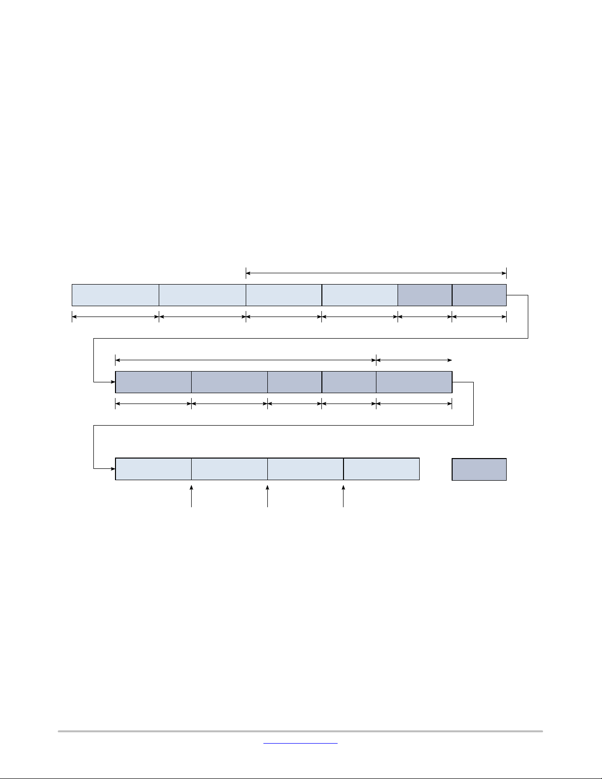
The AX5045 features a 256 Byte FIFO. The same FIFO
is used for both reception and transmission. During transmit,
only the write port is accessible by the microcontroller.
During receive, only the read port is accessible by the
microcontroller. Otherwise, both ports are accessible
through the register file.
In order to prevent transmitting premature data, the FIFO
contains three pointers. Data is read at the read pointer, up
to the write pointer. Data is written to the write ahead pointer .
The write pointer is not updated when data is written,
therefore, new data is not immediately visible to the
consumer. Writing the COMMIT command to the
FIFOSTAT register copies the write ahead pointer to the
write pointer, thus making the written data visible to the
Write ahead pointer
Write pointer
FIFOCOUNT
receiver. Writing the ROLLBACK command to the
FIFOSTAT register sets the write ahead pointer to the write
pointer, thus discarding data written to the FIFO. During
transmit, this means that the transmitter will only consider
data written to the FIFO after the commit command. During
receive, this feature is used by the receiver to store packet
data before it is known whether the CRC check passes.
FIFOCOUNT reports the number of bytes that can be read
without causing an underflow. FIFOFREE reports the
number of bytes that can be written without causing an
overflow. FIFOCOUNT and FIFOFREE do not add up to
256 Bytes whenever there are uncommitted bytes in the
FIFO. Figure 6 illustrates this.
256−FIFOFREE
Figure 6. FIFO Pointer
FIFO Chunk Encoding
In order to distinguish meta-data (such as RSSI) from
receive or transmit data, FIFO contents are organized as
chunks. Chunks consist of a header that encodes the chunk
length as well as the payload data format.
Each chunk starts with a single byte header. The header
encodes the length of a chunk, and indicates the data it
contains. The top 3 bits encode the length (or optionally refer
to an additional length byte after the header byte), and the
bottom 5 bits indicate what payload data the chunk contains.
The following table lists the encoding of the length bits (top
3 bits of the first chunk header byte). Figure 7 shows the
chunk header byte encoding.
Read pointer
76543210
Chunk
payload
size
Figure 7. FIFO Header byte Format
Chunk
payload
data format
The following table lists the chunk payload size encoding:
www.onsemi.com
7
Page 8
AND9902/D
100
Invalid
101
Invalid
110
Invalid
111
Variable length payload; payload size is encoded in the following length byte the length byte is part of
Table 4. CHUNK TYPES AND THEIR ENCODINGS
Hdr. Byte
7−0
No Payload Commands
T
00000000
No Operation
T
00000011
Trigger a Radiocontrol
One Byte Payload Commands
R
00110001
RSSI
T
00111100
Transmit Control
Two Byte Payload Commands
R
01010010
Frequency Offset
R
01010101
Background Noise
Three Byte Payload Commands
T
01100010
Repeat Data
TR
01110000
Timer
R
01110011
RF Frequency Offset
R
01110100
Datarate
R
01110101
Antenna Selection RSSI
Variable Length Payload Commands
TR
11100001
Data
T
11111101
Transmit Power
Table 5. NOP COMMAND
7654321
0
0000000
0
Table 6. FIFOIRQ COMMAND
7654321
0
0000001
1
Table 7. RSSI COMMAND
765432100011000
1
RSSI
Table 8. TXCTRL COMMAND
765432100011110
0
0
Table 3. CHUNK PAYLOAD SIZE ENCODING (continued)
Top Bits Chunk Payload Size
the header (and not included in length), everything after the length byte is included in the length
The following table lists the chunk types and their
encodings. The Hdr Byte column lists the complete FIFO
Chunk Header Byte, consisting of the length and data format
encodings.
Name Dir
NOP
FIFOIRQ
RSSI
TXCTRL
FREQOFFS
ANTRSSI2
REPEATDATA
TIMER
RFFREQOFFS
DATARATE
ANTRSSI3
Description
interrupt
(Antenna, Power Amp)
Calculation RSSI
FIFOIRQ Command
The FIFOIRQ command triggers an interrupt if bit
IRQMRADIOCTRL is set in register IRQMASK0 and bit
REVMFIFOIRQCMDDET is set in register
RADIOEVENTMASK. This feature allows to track TX
events as for example completion of preamble transmission.
To clear the interrupt, register RADIOEVENTREQ0 has
to be read.
RSSI Command
The RSSI command will only be generated by the receiver
at the end of a packet if bit ST RSSI is set in register
PKTSTOREFLAGS. The encoding is the same as that of the
RSSI register.
TXCTRL Command
DATA
TXPWR
Direction: T = Transmit, R = Receive
NOP Command
SETTX TXSE TXDIFF SETANT ANTSTATE SETPA PASTATE
The TXCTRL command allows certain aspects of the
transmitter to be changed on the fly. If SETTX is set, TXSE
and TXDIFF are copied into the register MODCFGA. If
SETANT is set, ANTSTATE is copied into register
DIVERSITY. If SETPA is set, PASTATE is copied into
register PWRAMP.
The NOP command will be discarded without effect by
the transmitter. The receiver will not generate NOP
commands.
www.onsemi.com
8
Page 9
AND9902/D
Table 9. FREQOFFS COMMAND
7654321
0
0101001
0
FREQOFFS1
FREQOFFS0
Table 10. ANTRSSI2 COMMAND
7654321
0
0101010
1
RSSI
BGNDNOISE
Table 11. REPEATDATA COMMAND
765432100110001
0
0
DIBITSYNC
UNENC
RAW
NOCRC
RESIDUE
PKTEND
PKTSTART
REPEATCNT
DATA
Table 12. TIMER COMMAND
7654321
0
0111000
0
TIMER2
TIMER1
TIMER0
Table 13. RFFREQOFFS COMMAND
765432100111001
1
RFFREQOFFS2
RFFREQOFFS1
RFFREQOFFS0
Table 14. DATARATE COMMAND
7654321
0
0111010
0
DATARATE2
DATARATE1
DATARATE0
FREQOFFS Command
The FREQOFFS command will only be generated by the
receiver at the end of a packet if bit ST FOFFS is set in
register PKTSTOREFLAGS. The encoding is the same as
that of the TRKFREQ register.
REPEATDATA Command
ANTRSSI2 Command
The ANTRSSI2 command will be generated by the
receiver when it is idle if bit ST ANT RSSI is set in register
PKTSTOREFLAGS. If DIVENA is set in register
DIVERSITY, the ANTRSSI3 command is generated
instead. The encoding of the RSSI field is the same as that
of the RSSI register. The BGNDNOISE field contains an
estimate of the background noise.
The REPEATDATA command allows the efficient
transmission of repetitive data bytes. The DATA byte given
in the payload is repeated REPEATCNT times. See DATA
command for a description of the flag byte. This command
is especially handy for constructing preambles.
TIMER Command
This command enables exact packet timing, e.g. for
frequency hopping systems.
In TX mode, upon detection of a TIMER command, the
transmitter pauses until the internal timer (accessible via
TIMER register) reaches the value given by the payload. A
detailed documentation of this function can be found under
the description of register RCTRLTIMESTAMP.
In RX mode, the TIMER command will be generated by
the receiver at the start/end of a packet if bit ST TIMER
and/or ST TIMER PKTEND is set in register
PKTSTOREFLAGS. The payload is a copy of the internal
timer (i.e. the current value of the TIMER register).
RFFREQOFFS Command
The RFFREQOFFS command will only be generated by
the receiver at the end of a packet if bit ST RFOFFS is set in
register PKTSTOREFLAGS. The encoding is the same as
that of the TRKRFFREQ register.
DATARATE Command
The DATARATE command will only be generated by the
receiver at the end of a packet if bit ST DR is set in register
PKTSTOREFLAGS. The encoding is the same as that of the
TRKDATARATE register.
www.onsemi.com
9
Page 10
AND9902/D
Table 15. ANTRSSI3 COMMAND
7654321
0
0111010
1
ANTORSSI2
ANTORSSI1
ANTORSSI0
Table 16. TRANSMIT DATA FORMAT
7654321
0
1110000
1
LENGTH
0
DIBITSYNC
UNENC
RAW
NOCRC
RESIDUE
PKTEND
PKTSTART
DATA
Table 17. FIFO COMMAND
0xE1
FIFO Command
0x04
Length Byte
0x24
Flag Byte: Unencoded, to ensure 0−1 remains 0−1, and Residue set, because the number of bits
0xAA
Alternating 0−1 bits
0xAA
Alternating 0−1 bits
0x1A
Alternating 0−1 bits; Bit 4 is the “Stop” bit
Table 18. RECEIVE DATA FORMAT
7654321
0
1110000
1
LENGTH
SYNCWD
ABORT
SIZEFAIL
ADDRFAIL
CRCFAIL
RESIDUE
PKTEND
PKTSTART
DATA
ANTRSSI3 Command
The ANTRSSI3 command will be generated by the
receiver when it is idle if bit ST ANT RSSI is set in register
LENGTH includes the flags byte as well as all DATA
bytes.
Setting RAW to one causes the DATA to bypass the
framing mode, but still pass through the encoder.
Setting UNENC to one causes the DATA to bypass the
framing mode, as well as the encoder, except for inversion.
UNENC has priority over RAW.
Setting NOCRC suppresses the generation of the CRC
bytes.
Setting RESIDUE allows the transmission of a number of
data bits that is not a multiple of eight. All but the last data
byte are transmitted as if RESIDUE was not set. The last
byte however contains only 7 bits or less. The transmitter
looks for the highest bit set. This is considered the stop bit.
Only bits below the stop bit are transmitted. If the
MSBFIRST in re g ister PKTADDRCFG is set, the algorithm
PKTSTOREFLAGS. If DIVENA is not set in register
DIVERSITY, the ANTRSSI2 command is generated
instead. The encoding of the ANT0RSSI and ANT1RSSI
fields are the same as that of the RSSI register.
The BGNDNOISE field contains an estimate of the
background noise.
DATA Command
The DATA command transports actual transmit and
receive data. While the basic format is the same for transmit
and receive, the semantics of the flag byte differs.
is reversed, i.e. the lowest bit set is considered the stop bit
and bits above the stop bit are transmitted.
PKTSTART and PKTEND bits enable the transmission of
packets that are larger than the FIFO size. If PKTSTART is
set, the radio packet starts at the beginning of the DATA
command payload. If PKTEND is set, the radio packet ends
at the end of the DA TA command payload. If PKTSTART is
not set, this command is the continuation of a previous
DATA command. If PKTEND is not set, the packet is
continued with the next DATA command.
Setting DIBITSYNC causes the DATA bytes to be aligned
to DiBit boundaries in 4−FSK mode.
For example, to transmit 20 bits of an alternating 0−1
pattern as a preamble, the following bytes should be written
to the FIFO (MSBFIRST = 0 in register PKTADDRCFG is
assumed):
transmitted is not a multiple of 8
www.onsemi.com
10
Page 11

AND9902/D
Table 19. TXPWR COMMAND
7654321
0
1111001
0
LENGTH = 10
TXPWRCOEFFA (7:0)
TXPWRCOEFFA (15:8)
TXPWRCOEFFB (7:0)
TXPWRCOEFFB (15:8)
TXPWRCOEFFC (7:0)
TXPWRCOEFFC (15:8)
TXPWRCOEFFD (7:0)
TXPWRCOEFFD (15:8)
TXPWRCOEFFE (7:0)
TXPWRCOEFFE (15:8)
ABOR T i s set if the packet has been aborted. An ABORT
sequence is a sequence of seven or more consecutive one bits
when HDLC [1] framing is used. Note that if ACCPT ABR T
is not set in register PKTACCEPTFLAGS, then aborted
packets are silently dropped.
SIZEFAIL is set if the packet does not pass the size
checks. Size checks are implemented using the
PKTLENCFG, PKTLENOFFSET and PKTMAXLEN
registers. Note that if ACCPT SZF is not set in register
PKTACCEPTFLAGS, then packets with an invalid size are
silently dropped.
ADDRFAIL is set if the packet does not pass the address
checks. Address checks are implemented using the
PKTADDRCFG, PKTADDRA, PKTADDRB,
PKTADDRENA and PKTADDRMASK registers. Note that
if ACCPTADDRF is not set in register
PKTACCEPTFLAGS, then packets which do not match the
programmed address are silently dropped.
CRCF AIL i s set if the packet does not pass the CRC check.
Note that if ACCPTCRCF is not set in register
PKTACCEPTFLAGS, then packets which fail the CRC
check are silently dropped.
RESIDUE, PKTEND and PKTSTART work identical as
in transmit mode, see above.
The receiver generates chunks up to PKTCHUNKSIZE
bytes. If PKTMAXLEN is larger than PKTCHUNKSIZE,
multiple chunks may be generated for one packet. Since
CRC and size checks may only be performed at the end of
the packet, only the last chunk can be dropped at failure of
one of those tests. It is therefore important that the
microcontroller receiver routine clears its receive buffer at
the beginning of DATA commands whose PKTSTART bit
is set, as the buffer may still contain bytes from erroneous
packets.
TXPWR Command
The TXPWR command allows the transmit power to be
changed on the fly. This command updates the
TXPWRCOEFFA, TXPWRCOEFFB, TXPWRCOEFFC,
TXPWRCOEFFD and TXPWRCOEFFE registers.
www.onsemi.com
11
Page 12

PROGRAMMING THE CHIP
Table 20. PWRMODE REGISTER STATES
PWRMODE register
Name
Description
Typical Idd
0000
POWERDOWN
Powerdown; all circuits powered down except for the register file
640 nA
0001
DEEPSLEEP
Deep Sleep Mode; Chip is fully powered down until SEL is lowered
121 nA
0101
STANDBY
Crystal Oscillator enabled
960μA
0111
FIFOON
FIFO enabled (Crystal Oscillator enabled by setting bit XOEN in
1010μA
1000
SYNTHRX
Synthesizer running, Receive Mode
7mA
1001
FULLRX
Receiver Running
14-17 mA
1011
WORRX
Receiver Wake-on-Radio Mode
700 nA
1100
SYNTHTX
Synthesizer running, Transmit Mode
7mA
1101
FULLTX
Transmitter Running at 23 dBm
255 mA
AND9902/D
Power Modes
To enable the lowest possible application power
consumption, the AX5045 allows to shut down its circuits
again; looses all register contents
register PWRMODE)
The following list explains the typical programming flow.
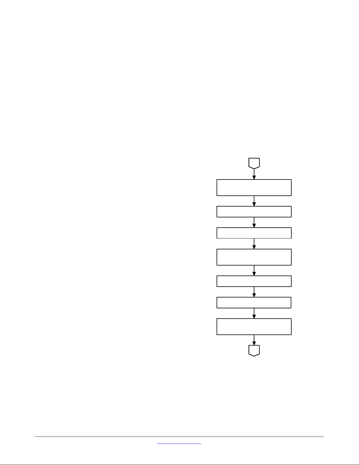
Preparation:
1. Reset the Chip. Set SEL to high for at least 1μs,
then low. Wait until MISO goes high. Set, and then
clear, the RST bit of register PWRMODE.
2. Set the PWRMODE register to POWERDOWN.
3. Program parameters. It is recommended that
suitable parameters are calculated using the
AX−RadioLab tool available at onsemi.com
.
4. Perform auto-ranging, to ensure the correct VCO
range setting.
The chip is now ready for transmit and receive operations.
FIFO Power Management
The FIFO is powered down during POWERDOWN and
DEEPSLEEP modes (Register PWRMODE). Reads to
register FIFOSTAT will provide bit FIFO EMPTY as one
and bit FIFO FULL as zero. Registers FIFOCOUNT and
FIFOFREE read zero as well. Reads from the FIFO will
return undefined data, and writes to the FIFO will be lost.
In the receive case, the FIFO is automatically powered on
when the chip PWRMODE is set to FULLRX. The FIFO
should be emptied before the PWRMODE is set to
POWERDOWN. In Wake-on-radio or POWERDOWN
when not needed. This is controlled by the PWRMODE
register. Idd values are typical; for exact values, please refer
to the AX5045 datasheet [2].
mode, the FIFO is automatically kept powered on until it is
emptied by the microprocessor.
In the transmit case, PWRMODE should first be set to
FULLTX. Before writing to the FIFO, the microprocessor
must ensure that the SVMODEM bit is high in Register
POWSTAT, to ensure that the on-chip voltage regulator
supplying the FIFO has finished starting up. The transmitter
remains idle until the contents of the FIFO are committed
(unless the FIFO AUTO COMMIT bit is set in Register
FIFOSTAT).
Autoranging
Whenever the frequency changes, the synthesizer VCO
should be set to the correct range using the built-in autoranging. A re-ranging of the VCO is required if the
frequency change required is la r ger than 0.5 MHz divided by
the RF Divider Ratio resulting from the RFDIV setting in
register PLLVCODIV. Each individual chip must be
auto-ranged. If both frequency register sets FREQA and
FREQB are used, then both frequencies must be auto-ranged
by first starting auto-ranging in PLLRANGINGA, waiting
for its completion, followed by starting auto-ranging in
PLLRANGINGB and waiting for its completion.
www.onsemi.com
12
Page 13
AND9902/D
Table 21. FUNDAMENTAL COMMUNICATION CHARACTERISTIC
Parameter
Description
f
Frequency of the connected crystal/TCXO in Hz
modulation
PSK, ASK, FSK, MSK, OQPSK, 4−FSK or AFSK (for recommendations see below)
f
Carrier frequency (i.e. center frequency of the signal) in Hz
BITRATE
Desired bit rate in bit/s
h
Modulation index, determines the frequency deviation for FSK
encoding
Inversion, differential, Manchester, scrambled, for recommendations see the description of the register
Table 22. TRADE-OFFS BETWEEN THE DIFFERENT MODULATION
Modulation
Trade-offs
FSK
For bit rates up to 125 kbit/s; 200 kbit/s possible with some limitations*
ASK
For bit rates up to 50 kbit/s;
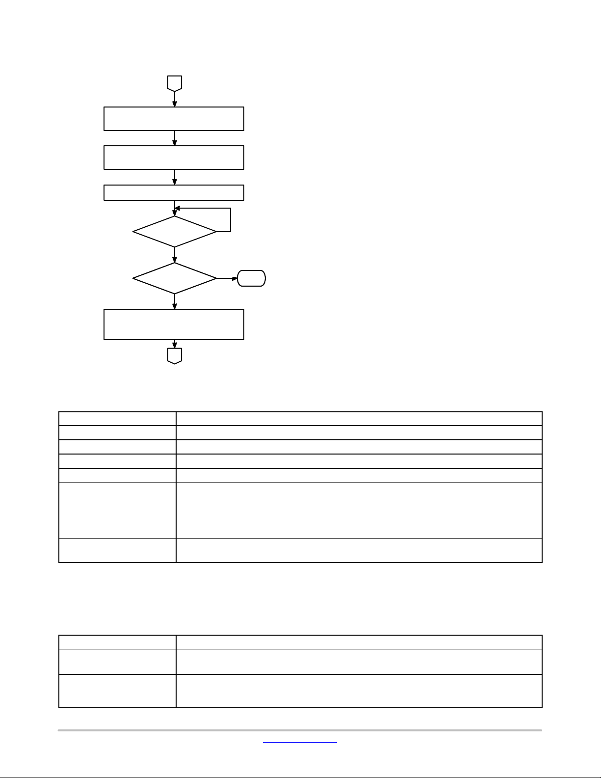
Figure 8 shows the flow chart of the auto-ranging process.
Set PWRMODE to STANDBY
Enable TCXO if used
Wait until crystal oscillator
Set RNGSTART of PLLRANGINGA/B
Set PWRMODE to POWERDOWN
is ready
RNGSTART = 1?
no
RNGERR = 1?
no
Disable TCXO if used
yes
yes
Error
Before starting the auto-ranging, the appropriate
frequency registers (FREQA or FREQB) need to be
programmed. Auto-ranging starts at the VCOR (register
PLLRANGINGA or PLLRANGINGB) setting;
if you already know the approximately correct synthesizer
VCO range, you should set VCORA/VCORB to this value
prior to starting auto-ranging; this can speed up the ranging
process considerably. The autoranging feature will not
increment/decrement the MSB so preset this to the
appropriate range prior to setting the RNGSTART bit.
Hardware clears the RNG START bit automatically as
soon as the ranging is finished; the device may be
programmed to deliver an interrupt on resetting of the RNG
START bit.
Waiting until auto-ranging terminates can be performed
by either polling the register PLLRANGINGA1 or
PLLRANGINGB1 for RNG START to go low, or by
enabling the IRQMPLLRNGDONE interrupt in register
IRQMASK1.
Choosing the Fundamental Communication
Characteristics
The following table lists the fundamental communication
characteristics that need to be chosen before the device can
be programmed.
Figure 8. Autoranging Flow Chart
XTAL
CARRIER
32 > h ≥ 0.5 for FSK, 4−FSK or AFSK, f
h = 0.5 for MSK and OQPSK
(For AFSK, f
often approximately 3 kHz)
ENCODING.
is usually set according to the FM channel specification. For 25 kHz channels, it is
deviation
The following table gives an overview of the trade-offs
between the different modulations that AX5045 offers, they
should be considered when making a choice.
= 0.5 * h * BITRATE
deviation
Frequency deviation is a free parameter
ASK is spectrally more efficient than FSK, but also more susceptible to noise and can only be
demodulated with lower sensitivity.
www.onsemi.com
13
Page 14

AND9902/D
MSK
For bit rates up to 125 kbit/s; 200 kbit/s possible with some limitations*
OQPSK
For bit rates up to 125 kbit/s; 200 kbit/s possible with some limitations*
PSK
For bit rates up to 10 kbit/s;
4−FSK
For bit rates up to 100 kSymbols/s, or 200 kbit/s possible with some limitations*
AFSK
For bit rates up to 25 kbit/s
x16+x12+x5+1
16
32
5
Table 22. TRADE-OFFS BETWEEN THE DIFFERENT MODULATION (continued)
Modulation Trade-offs
Robust and spectrally efficient form of FSK (Modulation is the same as FSK with h = 0.5)
Frequency deviation given by bit rate
The advantage of MSK over FSK is that it can be demodulated with higher sensitivity.
Slightly longer preambles required than for FSK
Very similar to MSK, with added precoding / postdecoding
For new designs, use MSK instead
Spectrally efficient and high sensitivity
Very accurate frequency reference (maximum carrier frequency deviation ±
preambles required
Similar to FSK, but four frequencies are used to transmit 2 bits simultaneously
Very slightly more spectrally efficient compared to FSK
((1 + 3 h/2) ⋅ BITRATE versus (1 + h) ⋅ BITRATE) for small h.
Longer preambles required as frequency offset estimation needs to be more precise to successfully
demodulate
For new designs, use FSK instead
Bits are FSK modulated in the audio band, then frequency modulated on the carrier frequency.
For legacy compatibility applications only.
*To receive at a data rate of 200 kbit/s, a reference clock between 32 and 50 MHz is required. The ADC clock needs to be configured to by 1/2
the reference clock. This causes the ADC to sample at 2 MSPS instead of 1 MSPS and is required for receiving at the higher data rates. The
ADC sample rate should still be configured as 2 MSPS in all setup configurations. Also, when receiving with higher datarates, care must be
taken to increase the RX bandwidth accordingly (see BBTUNE Register). Also note that the higher sample rate will result in increased current
consumption of 1−1.5 mA, due to increased clocking. In order to transmit at the higher data rates, care must be taken to ensure the PLL loop
bandwidth is wide enough to handle the modulation properly.
Given these fundamental physical layer parameters,
AX_RadioLab should be used to compute the register
settings of the AX5045.
Framing
Figure 1 shows the block diagram of the AX5045. After
the user writes a transmit packet into the FIFO, the Radio
Controller sequences the transmitter start-up, and signals the
Packet Controller to read the packet from the FIFO and add
framing bits, allowing the receiver to lock to the transmit
waveform, and to detect packet and byte boundaries. If MSB
first is selected (register PKTADDRCFG), then the bits
within each byte are swapped when the data is read out from
the FIFO.
The Packet Controller also (optionally) adds cyclic
redundancy check (CRC) bits at the end of the packet, to
enable the receiver to detect transmission errors. Both 16
and 32 Bit CRC can be selected, as well as different
generator polynomials. The CRC polynomial can be
selected in register CRCCFG. The following polynomials
are supported:
• CRC-CCITT (16bit):
(hexadecimal: 0x1021)
• CRC-16 (16bit):
x
+ x15+ x2+1
(hexadecimal: 0x8005)
1
/4 ⋅ BITRATE) and long
• CRC-DNP (16bit):
16
+ x13+ x12+ x11+ x10+ x8+ x6+ x5+ x2+1
x
(hexadecimal: 0x3D65)
This polynomial is used for Wireless M-Bus.
• CRC-32 (32bit):
x
+ x26+ x23+ x22+ x16+ x12+ x11+ x10+ x8+ x7+
4
5
x
+
x
+ x2+x+
(hexadecimal: 0x04C11DB7)
1
The CRC is always transmitted MSB first regardless of
the MSB first setting of register PKTADDRCFG, to enable
the receiver to process CRC bits as they arrive (otherwise,
they would have to be stored and reordered). For an in-depth
guide on how CRC’s are computed, see [3].
By default, the CRC bits are inverted so that erroneously
appended zero−bits can be detected. Skipping this inversion
is not recommended, but it can be achieved by setting bit
CRCNOINV in register CRCCFG.
Finally, the encoder is able to perform certain bit-wise
operations on the bit-stream:
• Manchester:
Manchester transmits a one bit as 10 and a zero bit as
01, i.e. it doubles the data rate on the radio channel. Its
advantage is that the resulting bit-stream has many
transitions and thus simplifies synchronizing to the
www.onsemi.com
14
Page 15
AND9902/D
transmission on the receiver side. The downside is that
it now requires twice the amount of energy for the
transmission. Manchester is not recommended, except
for compatibility with legacy systems.
• Scrambler:
The scrambler ensures that even highly regular transmit
data results in a seemingly random transmitted
bit-stream. This avoids discrete tones in the spectrum.
Three different scrambling polynomials can be selected
(PN9, PN15, PN17) and it is possible to choose
between additive or multiplicative (self−synchronizing)
scrambling. Do not confuse the scrambler with
encryption – it does not provide any secrecy, its actions
are easily reversed. Its use is recommended, particularly
multiplicative scrambling.
• Differential:
Differential transmits zero bits as constant level, and
one bits as level change. This allows to accommodate
modulations that can invert the bit-stream, such as PSK.
• Inversion:
If on, the bit-stream is inverted. Useful for example for
compatibility with legacy systems, such as POCSAG,
which differ from the usual convention that the higher
FSK frequency signifies a one.
powers up the synthesizer and settles it (registers
TMGTXBOOST and TMGTXSETTLE determine the
timing). The Preamble and the Packet(s) are then
transmitted, followed by the transmitter and synthesizer
shut-down.
The transmitter is automatically ramped up and down
smoothly, to prevent unwanted spurious emissions. The
ramp time is normally one bit time, but may be longer by
changing the SLOWRAMP field of register MODCFGA.
The PWRMODE register should stay at FULLTX until
the transmission is fully completed. The end of the
transmission may be determined by polling the register
RADIOSTATE until it indicates idle, or by enabling the
radio controller interrupt (bit IRQMRADIOCTRL) in
register IRQMASK0 and setting the radio controller to
signal an interrupt at the end of transmission (bit
REVMDONE of register RADIOEVENTMASK0).
Set PWRMODE to FULLTX
Enable TCXO if used
The encoder is controlled using the register ENCODING.
It may be temporarily bypassed except for the inversion by
setting the UNENC bit of the FIFO chunks DATA or
REPEATDATA. This is useful for synthesizing preambles.
The receiver performs these tasks in reverse order.
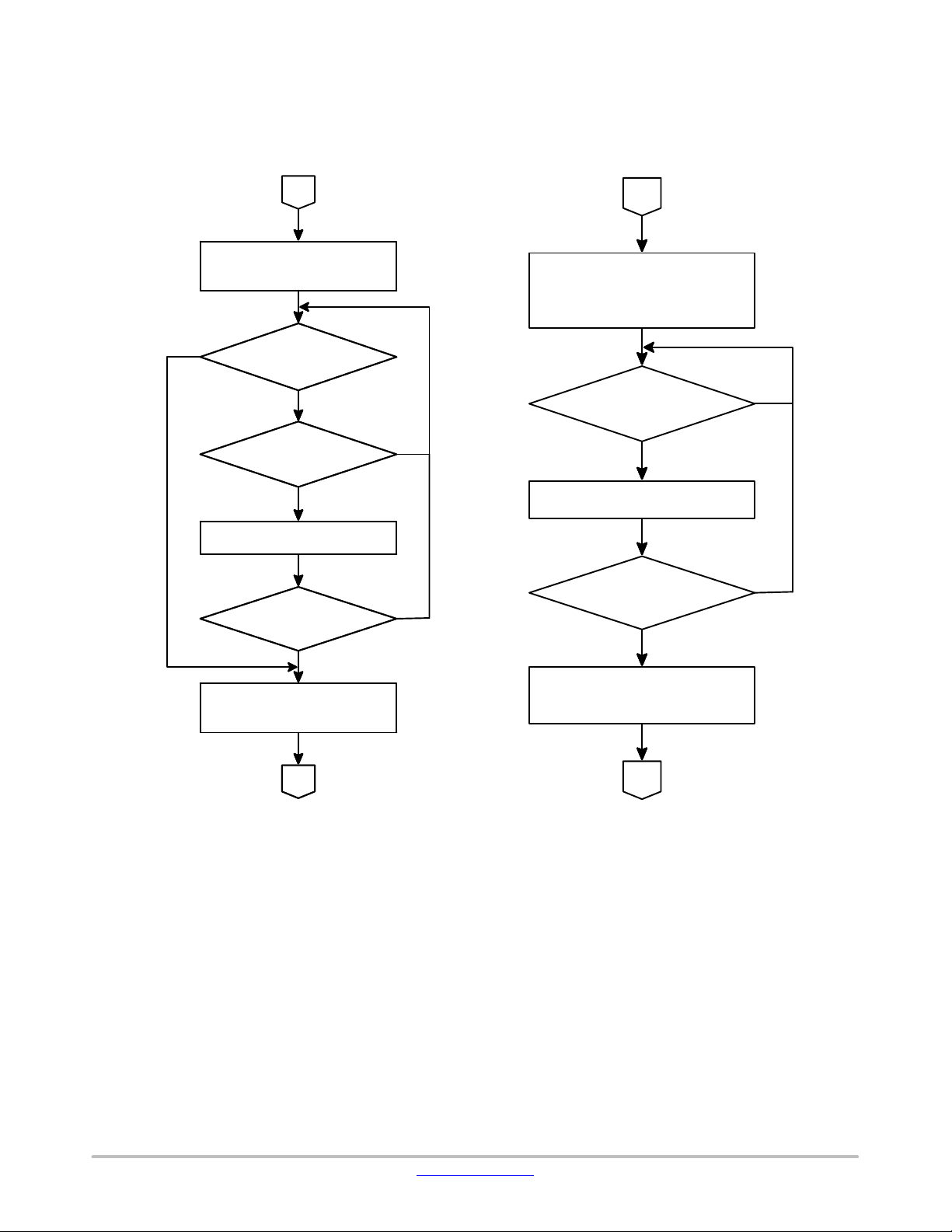
Transmitter
Figure 9 shows the transmitter flow chart. The
microprocessor first places the chip into FULLTX mode.
This prepares the chip for a future transmission, enables the
FIFO in transmit direction, but does not yet power-up the
synthesizer or any other transmit circuitry.
The microprocessor can now write the preamble and the
actual packet to the FIFO. The preamble is programmable to
allow standards to be implemented that specify a specific
preamble to be used. Otherwise, the recommendations for
preambles can be found below.
Waiting for the crystal oscillator to start up may be
performed by polling the register XTALSTATUS, or by
enabling the IRQMXTALREADY interrupt in register
IRQMASK1.
After the FIFO contents are committed (writing the
Commit command to the FIFOSTAT register), the
transmitter notices that the FIFO is no longer empty. It then
Write Preamble to FIFO
Write Packet to FIFO
Wait until crystal oscillator
Wait until transmission is done
Set PWRMODE to POWERDOWN
Figure 9. Transmitter Flow Chart
is running
Commit FIFO
Disable TCXO if used
www.onsemi.com
15
Page 16

AND9902/D
Recommended Preamble
The main purpose of the preamble is to allow for the
receiver to acquire vital transmission parameters before the
actual packet data starts. The minimum duration of the
preamble is dependent on how much time the receiver needs
to acquire these parameters to sufficient precision. More
specifically, it depends on:
• The time needed for the receiver adaptive gain control
(AGC) to acquire the signal strength.
• The time needed for the receiver to acquire the
maximum possible frequency offset
(register MAXRFOFFSET).
• The time needed for the receiver to acquire the
maximum possible data rate offset
(register MAXDROFFSET).
• The time needed for the receiver to acquire the exact bit
sampling time (register TIMEGAIN).
• The time needed to acquire the actual frequency
deviation in 4−FSK mode (register FSKDMAX).
On the AX5045, these loops run in parallel. An AGC that
is significantly off however causes the received signal to fall
outside the IF strip dynamic range, and thus prevents the
other loops from working. And a frequency offset that is
compensated insufficiently causes the received signal to fall
(partially) outside the IF filter, thus also preventing the
timing and 4−FSK loops from working.
The minimum possible preamble duration can be
achieved under the following conditions:
• Use a transmitter with a sufficiently precise bit timing.
If the maximum deviation of the transmitter data rate
from the receiver data rate is less than approximately
0.1%, then the data rate acquisition loop should be
switched off completely (setting register
MAXDROFFSET to zero). The AX5045 is able to
track the remaining small offset without the data rate
offset loop. All ON Semiconductor transmitters of the
AX504x family derive the bit rate timing from the
crystal reference and can therefore easily meet this
requirement.
• Use an FSK frequency deviation that is larger than the
maximum frequency offset between transmitter and
receiver. In this case, receiver frequency offset
acquisition is not needed. Do not use 4−FSK.
• Use the AX5045 receiver parameter set feature, below.
Finally, the frame synchronization word achieves byte
synchronization.
The recommended preamble bit pattern is now discussed.
If the standard to be implemented requires a specific
preamble, use it.
In FEC mode, HDLC [1] flags (pattern 01 111110) must be
transmitted. The convolutional encoder ensures enough bit
transitions, and the AX5045 receiver needs flags to
synchronize its interleaver.
If multiplicative scrambling or Manchester is enabled,
send RAW bytes 00010001. The scrambler or Manchester
encoder ensure enough transitions to acquire the bit timing.
In 4−FSK mode, send UNENCODED bytes 00010001.
This ensures that the preamble toggles between the highest
and the lowest frequency. The frequent transitions ensure the
bit timing is acquired as quickly as possible, and the
maximum and minimum frequencies allow the deviation to
be acquired. If inversion is enabled, make sure to set a
preamble that still results in toggling between DiBit symbols
of 10 and 00.
Otherwise, use UNENCODED 01010101. This preamble
ensures the maximum number of transitions for bit timing
synchronization. This preamble could also be used with the
multiplicative scrambler enabled; the main purpose of the
scrambler is however to ensure no spectral lines (tones), this
would be defeated by this preamble.
If MSBFIRST in register PKTADDRCFG is set, then the
preamble sequences should be reversed.
www.onsemi.com
16
Page 17
AND9902/D
Receiver
Figure 10 shows the receiver flow chart. When the
microprocessor places the chip into FULLRX mode, the
AX5045 immediately powers up the synthesizer, settles it
Set PWRMODE to FULLRX
Enable TCXO if used
yes
Timeout?
no
no
Packet Received?
(FIFO not empty)
yes
Read Packet from FIFO
(registers TMGRXBOOST and TMGRXSETTLE
determine the timing) and starts receiving. The reception
continues until the microprocessor changes the PWRMODE
register.
Set PWRMODE to WORRX
TCXO controlled by PWRAMP or
ANTSEL if used
no
Packet Received?
(FIFO not empty)
yes
Read Packet from FIFO
Continue
yes
Reception?
no
Set PWRMODE to POWERDOWN
Disable TCXO if used
Figure 10. Receiver Flow Chart
If antenna diversity is enabled, the AX5045 continuously
switches between the antennas (controlled by the ANTSEL
pin) to find the antenna with the better signal strength, until
a valid preamble is detected. Antenna scanning is resumed
after a packet is completed.
Actual packet data in the FIFO may be preceded and
followed by meta-data. Meta-data may be a time stamp at the
beginning and/or the end of the packet, and signal strength,
frequency offset and data rate offset at the end of the packet.
Which meta-data is written to the FIFO is controlled by the
register PKTSTOREFLAGS.
Wake-on-Radio mode allows the AX5045 to periodically
poll the radio channel for a transmission while using only
very little power. Figure 11 shows the wake-on-radio flow
yes
Continue
Reception?
no
Set PWRMODE to POWERDOWN
Disable TCXO if used
Figure 11. Wake-on-Radio Receiver Flow Chart
chart. The AX5045 periodically wakes up. The wake-up is
controlled by the on-chip low-power 640 Hz/10 kHz RC
oscillator and the period is programmed using the
WAKEUPFREQ register.
After waking up, the AX5045 quickly settles the AGC and
computes the channel RSSI. If it is below an absolute
threshold (register RSSIABSTHR) and a dynamic threshold
(register BGNDRSSITHR), it is switched off immediately.
Otherwise, it looks for a valid preamble. If none is found
within a preprogrammed time (registers TMGRXPREAMBLE1 and TMGRXPREAMBLE2), the receiver is powered
down. Otherwise, it continues to receive the packet.
www.onsemi.com
17
Page 18
AND9902/D
If a packet is successfully received, the receiver may
either be shut down again, or continue to run if
WORMULTIPKT is set in register PKTMISCFLAGS.
In Wake-on-Radio mode, the AX5045 is completely
autonomous until a packet is received. The microprocessor
may be shut down and only wake up once the FIFO is no
longer empty (IRQMFIFONOTEMPTY interrupt in
register IRQMASK0).
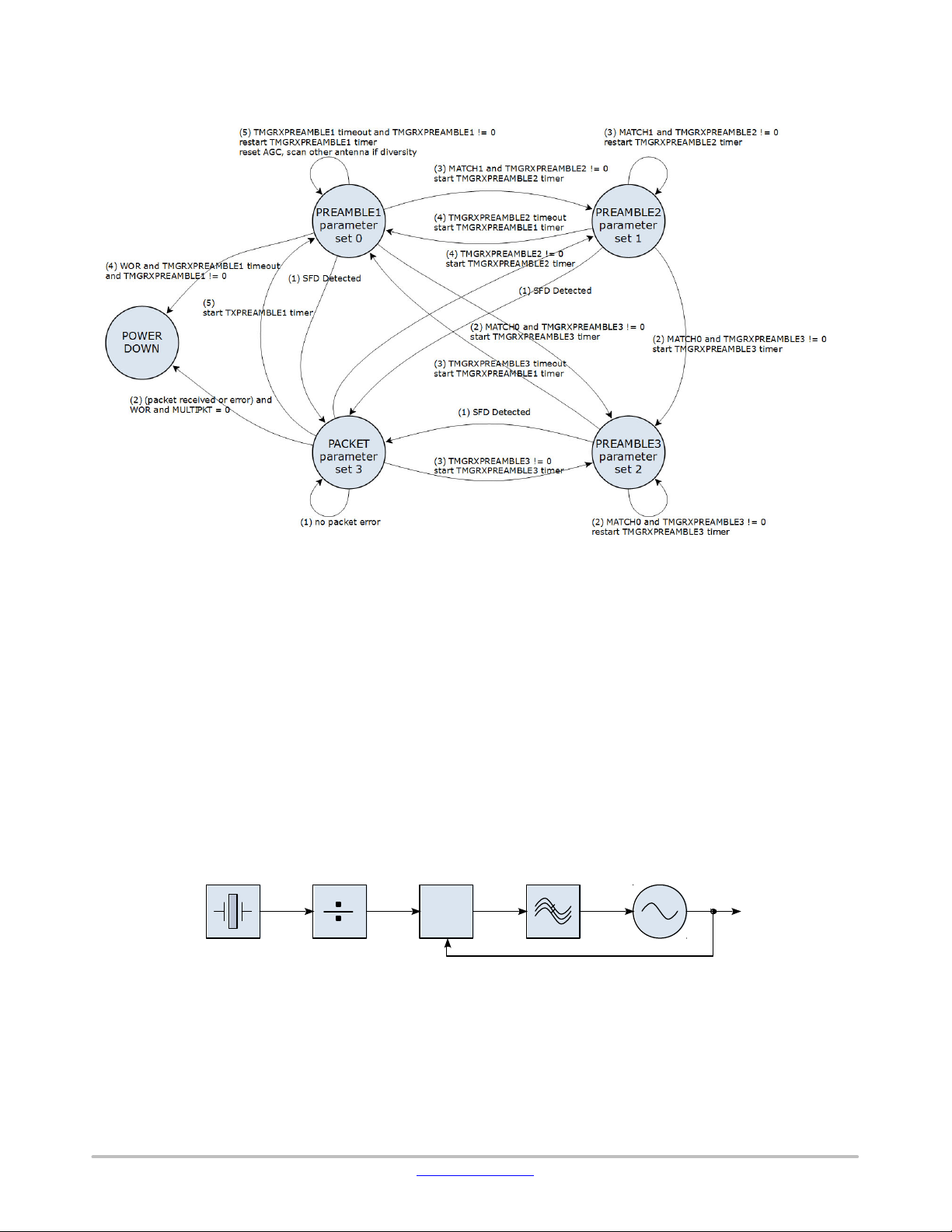
Receiver State Machine
Figure 12 shows the receiver timing diagram. The actions
in the first two lines are time controlled. The arrows below
indicate which register controls the timing. The actions
colored in a darker shade of blue are only performed when
diversity mode is enabled (DIVENA is set in register
DIVERSITY). The actions in the last line are detailed in the
state diagram Figure 13.
SYNTHBOOST and SYNTHSETTLE form the two
stage procedure to settle the synthesizer on the first LO
frequency. During SYNTHBOOST, the synthesizer is
operated at a higher loop bandwidth (register
PLLLOOPBOOST), while during SYNTHSETTLE, the
final settling is done at the nominal, lower noise, loop
bandwidth (register PLLLOOP).
IFINIT settles the IF strip. COARSEAGC uses a fast AGC
time constant to quickly settle the AGC to a value close to
the correct one. This is especially important during
wake-on-radio, as it is desirable to keep the receiver
powered the shortest possible time to save power. AGC
settles the AGC using a slower time constant. RSSI
measures the received signal strength. This value is then
used to determine whether the receiver should be kept
running in wake-on-radio, or to select the antenna with the
stronger signal in diversity mode.
Antenna #0
SYNTHBOOST SYNTHSETTLE IFINIT COARSEAGC AGC RSSI
TMGRXBOOST TMGRXSETTLE TMGRXOFFSACQ TMGRXCOARSEAGC TMGRXAGC TMGRXRSSI
Antenna #1 Selected Antenna
IFINIT COARSEAGC AGC RSSI IFINIT
TMGRXOFFSACQ TMGRXCOARSEAGC TMGRXAGC TMGRXRSSI TMGRXOFFSACQ
PREAMBLE1 PREAMBLE2 PREAMBLE3 PACKET
MATCH0MATCH1 SFD detected
Figure 12. Receiver Flow Chart
Once the receiver is initialized, PREAMBLE1,
PREAMBLE2, PREAMBLE3, and PACKET coordinate
the reception of packets. The receiver contains several loops
that acquire and track transmission parameters the receiver
needs to know in order to correctly receive a packet.
• The AGC acquires and tracks the signal strength
• The frequency tracking loop acquires and tracks the
frequency offset
• The timing and data rate tracking loop acquires and
tracks the sampling time and the data rate offset
The bandwidth of these loops is programmable. The
bandwidth controls the acquisition time as well as the
Antenna
Diversity only
noisiness of the parameter estimates. In order to allow both
fast acquisition to enable short preambles and low steady
state noise performance to enable high receiver sensitivity,
the receiver supports multiple acquisition and tracking loop
parameter sets. When the receiver searches for a
transmission signal, it uses wide loop bandwidths. Once it
detects a preamble with sufficient probability, it switches to
a lower loop bandwidth. Once a frame start is detected, it
switches to an even lower loop bandwidth. Figure 13 shows
the state diagram that controls which receiver parameter set
is used.
www.onsemi.com
18
Page 19
AND9902/D
Crystal
or TCXO
LPOSCREF
FD
LPOSCKFILT LPOSCFREQ
Figure 13. Receiver State Diagram
Conditions are evaluated in priority order. The priority
number is given in parentheses at the beginning of arrow
labels.
In order to reduce the number of registers that need to be
programmed if not all parameter sets are different, the
parameter set number of Figure 13 is not directly used to
address the parameter set. Instead, it indexes into register
RXPARAMSETS, where the actual parameter set number is
read out.
Low Power Oscillator Calibration
The low power oscillator is used to control the wake-up
frequency , o r polling period, during wake-on-radio mode. In
Figure 14. Low Power Oscillator Calibration Logic
order to increase the precision of the wake-up frequency,
calibration logic allows the low power oscillator to be
calibrated against the crystal oscillator or TCXO.
Figure 14 shows a block diagram of the calibration logic.
It works similarly to a PLL. The reference frequency from
the crystal or TCXO is divided by the value of the
LPOSCREF register. This signal is then compared to the
actual frequency of the Low Power Oscillator. The
frequency difference is then low pass filtered
(LPOSCKFILT register) and used to adjust the Low Power
Oscillator frequency (LPOSCFREQ register).
When enabled (LPOSCCALIBR or LPOSCCALIBF
enabled in register LPOSCCONFIG), the calibration logic
is only activated when the crystal oscillator or TCXO is
www.onsemi.com
enabled as well. This allows “opportunistic” calibration –
the Low Power Oscillator is calibrated whenever the
reference frequency is enabled.
19
Page 20
AND9902/D
PWRAMP
or ANTSEL
R
C
GND
DAC Voltage
Auxiliary DAC
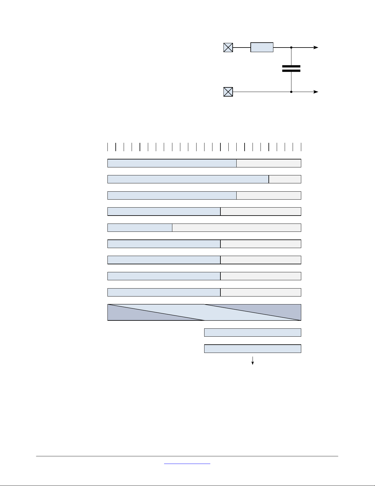
The AX5045 contains an auxiliary DAC. It can be used to
output various receiver signals, such as RSSI or Frequency
Offset, or just a value under program control. The DAC
signal can be output either on the PWRAMP or ANTSEL
pad.
The DAC may be operated in two modes. ΣΔ mode
employs a digital modulator to output a high resolution
signal. Its output voltage range is ¼ VDDIO to ¾ VDDIO
for a DACVALUE range from *2048 to 2047.
PWM mode outputs a pulse width modulated signal. It is
only suitable for low frequency signals. Its output voltage
range is 0 to VDDIO for a DACVALUE range from *2048
to 2047.
Figure 15. DAC RC Filter
A low pass filter, such as a simple R-C filter as shown in
Figure 15, must be used to obtain the analog voltage.
DACINPUT
0001
0010
0011
0100
0110
0111
1000
1001
1100
23 22 21 20 19 18 17 16 15 14 13 12 11 10 9 8 7 6 5 4 3 2 1 0
15
19
15
13
13
13
13
13
TRK_AMPLITUDE + 0x8000
TRK_RFFREQUENCY
TRK_FREQUENCY
TRK_FSKDEMOD
7
RSSI
0
0000 000000
SOFTDATA
I
Q
GPADC + 0x2000
0
00000000
0
0000
0
00000000
0
0000000000
000000
0
0
0
0
0000000000
0000000000
0000000000
0000000000
Shifter
register DACCONFIG selects the source signal. The input
signals are left aligned to 24 bits and padded with zeros. A
signed shifter then shifts the selected value to the right by 0
to 15 digits as selected by the lower four bits of the
DACVALUE register. The signal is then limited to the DAC
0000
Figure 16. DAC Signal Scaling
Figure 16 shows the DAC Signal scaling. DACINPUT in
www.onsemi.com
11
11
Limiter
DACVALUE
0
0
to DAC
value range of *2
11
to 211*1. This signal is then sent to the
DAC core. Note that if DACVALUE is selected as input, the
register value is directly sent to the DAC, the shifter is not
used. In fact, DACVALUE and DACSHIFT share the same
register bits.
20
Page 21
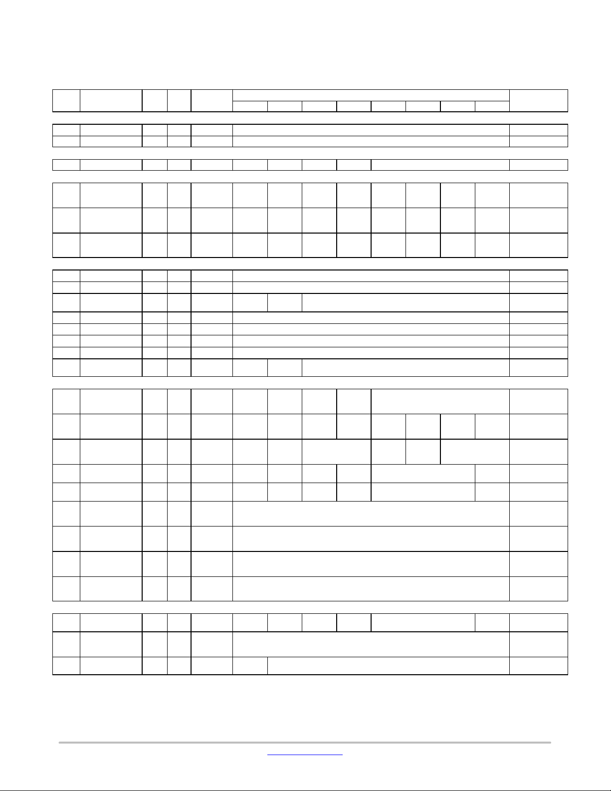
REGISTER OVERVIEW
Table 23. CONTROL REGISTER MAP
Bit
7654321
0
Revision & Interface Probing
000
REVISION
RR01000110
SILICONREV(7:0)
Silicon Revision
001
SCRATCH
RWR11000101
SCRATCH(7:0)
Scratch Register
Operating Mode
002
PWRMODE
RWR000–0000
RST
XOEN
REFEN
WDS
PWRMODE(3:0)
Power Mode
Voltage Regulator
003
POWSTAT
RR––––––––
SSUM
SREF
SVREF
SVANA
SVMO
SBEVA
SBEVM
SVIO
Power
004
RR––––––––
SSSUM
SSREF
SSVRE
SSVANASSVM
SSBEV
SSBEV
SSVIO
Power
005
POWIRQMASK
RWR00000000
MPWR
MSREF
MSVREFMS
MSBE
MSBE
MSVIO
Power
Interrupt Control
006
IRQMASK1
RWR00000000
IRQMASK(15:8)
IRQ Mask
007
IRQMASK0
RWR00000000
IRQMASK(7:0)
IRQ Mask
009
RWR––000000
––RADIO EVENT MASK(5:0)
Radio Event
00A
IRQINVERSION1
RWR00000000
IRQINVERSION(15:8)
IRQ Inversion
00B
RWR00000000
IRQINVERSION(7:0)
IRQ Inversion
00C
IRQREQUEST1
RR––––––––
IRQREQUEST(15:8)
IRQ Request
00D
IRQREQUEST0
RR––––––––
IRQREQUEST(7:0)
IRQ Request
00F
R
––––––––
––RADIO EVENT REQ(5:0)
Radio Event
Modulation & Framing
010
MODULATION
RWR–––01000
–––
RX
MODULATION(3:0)
Modulation
011
ENCODING1
RWR–––––––0
–––––––
ENC
Encoder/Decod
012
ENCODING0
RWR00000100
ENC
ENC
ENC SCRPOLY(1:0)
ENC
ENC
ENC INV(1:0)
Encoder/Decod
013
FRAMING
RWR––––0000
FRMRX–––
FRMMODE(2:0)
FABOR
Framing settings
014
CRCCFG
RWR––––0000
––––CRCMODE(2:0)
CRCN
CRC settings
015
CRCINIT3
RWR11111111
CRCINIT(31:24)
CRC
016
CRCINIT2
RWR11111111
CRCINIT(23:16)
CRC
017
CRCINIT1
RWR11111111
CRCINIT(15:8)
CRC
018
CRCINIT0
RWR11111111
CRCINIT(7:0)
CRC
Forward Error Correction
019
FECRWR
00000000
SHOR
RSTVI
FEC
FEC
FECINPSHIFT(2:0)
FEC
FEC (Viterbi)
01A
FECSYNC
RWR01100010
FECSYNC(7:0)
Interleaver
01B
FECSTATUS
RR––––––––
FEC
MAXMETRIC(6:0)
FEC Status
AND9902/D
Addr Name Dir Ret Reset
POWSTICKYSTAT
RADIOEVENTMASK
IRQINVERSION0
RADIOEVENTREQ
GOOD
Description
DEM
F
VANAMSVMOD
ODEM
EM
NA
ANA
VANA
ODEM
MODEM
VMOD
EM
Management
Status
Management
Sticky Status
Management
Interrupt Mask
Mask
Request
ALTPN
9
T MEM
INV
SCRM
ODE
TERBI
NEG
HALF
SPEED
POS
MANC
H
DIFF
NOSY
NC
T
OINV
ENA
er Settings
er Settings
Initialization
Data
Initialization
Data
Initialization
Data
Initialization
Data
Configuration
Synchronization
Threshold
www.onsemi.com
21
Page 22

AND9902/D
Status
01C
RADIOSTATE
R–––––0000
––––RADIOSTATE(3:0)
Radio Controller
01D
XTALSTATUS
RR––––––––
–––––––
XTAL
Crystal
Pin Configuration
020
PINSTATE
RR––––––––
––PS
PS
PS IRQ
PS
Pinstate
021
RWR1––00010
PU
––PFSYSCLK(4:0)
SYSCLK Pin
022
PINFUNCDCLK
RWR00–––100
PU
–––
PFDCLK(2:0)
DCLK Pin
023
PINFUNCDATA
RWR10–––111
PU
–––
PFDATA(2:0)
DATA Pin
024
PINFUNCIRQ
RWR00–––011
PU
PI IRQ–––PFIRQ(2:0)
IRQ Pin
025
RWR00–––110
PU
PI
–––
PFANTSEL(2:0)
ANTSEL Pin
026
RWR00––0110
PU
PI
––PFPWRAMP(3:0)
PWRAMP Pin
027
PWRAMP
RWR–––––––0
–––––––
PWRAMPPWRAMP
FIFO
028
FIFOSTAT
RR0–––––––
FIFO
–
FIFO
FIFO
FIFO
FIFO
FIFO
FIFO
FIFO Control
WRFIFOCMD(5:0)
029
FIFODATA
RW
––––––––
FIFODATA(7:0)
FIFO Data
02A
FIFOCOUNT1
RR–––––––0
–––––––
FIFO
Number of
02B
FIFOCOUNT0
RR00000000
FIFOCOUNT(7:0)
Number of
02C
FIFOFREE1
RR–––––––1
–––––––
FIFO
Number of
02D
FIFOFREE0
RR00000000
FIFOFREE(7:0)
Number of
02F
FIFOTHRESH
RWR00000000
FIFOTHRESH(7:0)
FIFO Threshold
Synthesizer
030
PLLLOOP
RWR0–––1001
FREQB–––
DIRECTFILTENFLT(1:0)
PLL Loop Filter
031
PLLCPI
RWR00001000
PLLCPI
PLL Charge
032
PLLRANGINGA1
RWR00000001
STICK
PLL
RNGERRRNG
STICK
VTUNE
–
VCOR
PLL
033
PLLRANGINGA0
RWR00000000
VCORA(7:0)
PLL
034
FREQA3
RWR00111001
FREQA(31:24)
Synthesizer
035
FREQA2
RWR00110100
FREQA(23:16)
Synthesizer
036
FREQA1
RWR11001100
FREQA(15:8)
Synthesizer
037
FREQA0
RWR11001101
FREQA(7:0)
Synthesizer
038
PLLLOOPBOOST
RWR0–––1011
FREQB–––
DIRECTFILTENFLT(1:0)
PLL Loop Filter
Table 23. CONTROL REGISTER MAP (continued)
Bit
Addr Description
ResetRetDirName
01234567
State
PINFUNCSYSCLK
PINFUNCANTSEL
PINFUNCPWRAMP
SYSCL
K
DCLKPIDCLK
DATAPIDATA
IRQ
ANTSE
L
PWRA
MP
AUTO
COMMI
T
ANTSE
L
PWRA
MP
PWR
AMP
FREE
THR
ANT
SEL
CNT
THR
OVER
RUN
DATAPSDCLKPSSYS
UNDE
R
FULL
CLK
EMPT
Y
COUN
T(8)
Oscillator Status
Function
Function
Function
Function
Function
Function
Control
Words currently
in FIFO
Y
LOCK
LOCK
START
Y
OFFR
NG
OFFR
NG
FREE(
8)
A(8)
Words currently
in FIFO
Words that can
be written to
FIFO
Words that can
be written to
FIFO
Settings
Pump Current
Autoranging
Autoranging
Frequency
Frequency
Frequency
Frequency
Settings
(Boosted)
www.onsemi.com
22
Page 23

AND9902/D
039
PLLCPIBOOST
RWR11001000
PLLCPI
PLL Charge
03A
PLLRANGINGB1
RWR00000001
STICK
PLL
RNGERRRNG
STICK
VTUNE
–
VCOR
PLL
03B
PLLRANGINGB0
RWR00000000
VCORB(7:0)
PLL
03C
FREQB3
RWR00111001
FREQB(31:24)
Synthesizer
03D
FREQB2
RWR00110100
FREQB(23:16)
Synthesizer
03E
FREQB1
RWR11001100
FREQB(15:8)
Synthesizer
03F
FREQB0
RWR11001101
FREQB(7:0)
Synthesizer
040
PLLVCODIV
RWR–––00000
–––
RFDIV
REFDIV(1:0)
PLL Divider
Signal Strength
041
RSSIRR
––––––––
RSSI(7:0)
Received Signal
042
BGNDRSSI
RWR00000000
BGNDRSSI(7:0)
Background
043
DIVERSITY
RWR––––––00
––––––ANT
DIV
Antenna
044
AGCCOUNTER
RWR––––––––
AGCCOUNTER(7:0)
AGC Current
Receiver Tracking
045
TRKDATARATE2
RR––––––––
TRKDATARATE(23:16)
Datarate
046
TRKDATARATE1
RR––––––––
TRKDATARATE(15:8)
Datarate
047
TRKDATARATE0
RR––––––––
TRKDATARATE(7:0)
Datarate
048
TRKAMPL1
RR––––––––
TRKAMPL(15:8)
Amplitude
049
TRKAMPL0
RR––––––––
TRKAMPL(7:0)
Amplitude
04A
TRKPHASE1
RR––––––––
––––TRKPHASE(11:8)
Phase Tracking
04B
TRKPHASE0
RR––––––––
TRKPHASE(7:0)
Phase Tracking
04D
TRKRFFREQ2
RWR––––––––
––––TRKRFFREQ(19:16)
RF Frequency
04E
TRKRFFREQ1
RWR––––––––
TRKRFFREQ(15:8)
RF Frequency
04F
TRKRFFREQ0
RWR––––––––
TRKRFFREQ(7:0)
RF Frequency
050
TRKFREQ1
RWR––––––––
TRKFREQ(15:8)
Frequency
051
TRKFREQ0
RWR––––––––
TRKFREQ(7:0)
Frequency
052
TRKFSKDEMOD1
RR––––––––
––TRKFSKDEMOD(13:8)
FSK
053
TRKFSKDEMOD0
RR––––––––
TRKFSKDEMOD(7:0)
FSK
054
RR––––––––
TRKAFSKDEMOD(15:8)
AFSK
055
RR––––––––
TRKAFSKDEMOD(7:0)
AFSK
Timer
059
TIMER2
R–––––––––
TIMER(23:16)
1MHz Timer
05A
TIMER1
R–––––––––
TIMER(15:8)
1MHz Timer
05B
TIMER0
R–––––––––
TIMER(7:0)
1MHz Timer
Table 23. CONTROL REGISTER MAP (continued)
Bit
Addr Description
ResetRetDirName
01234567
Pump Current
(Boosted)
Y
LOCK
LOCK
START
Y
OFFR
NG
OFFR
NG
SEL
B(8)
ENA
Autoranging
Autoranging
Frequency
Frequency
Frequency
Frequency
Settings
Strength
Indicator
RSSI
Diversity
Configuration
Value
Tracking
Tracking
TRKAFSKDEMOD1
TRKAFSKDEMOD0
Tracking
Tracking
Tracking
Tracking
Tracking
Tracking
Tracking
Tracking
Demodulator
Tracking
Demodulator
Tracking
Demodulator
Tracking
Demodulator
Tracking
www.onsemi.com
23
Page 24

AND9902/D
05C
TIMERCLK
RWR––––––10
––––––CLKMUX(1:0)
Internal Timer
Time Stamp
060
RWR00000000
RCTRLTIMESTAMP(23:16)
Radio Controller
061
RWR00000000
RCTRLTIMESTAMP(15:8)
Radio Controller
062
RWR00000000
RCTRLTIMESTAMP(7:0)
Radio Controller
064
RWR–––––––0
–––––––
TIMET
Radio Controller
Wakeup Timer
068
WAKEUPTIMER1
RR––––––––
WAKEUPTIMER(15:8)
Wakeup Timer
069
WAKEUPTIMER0
RR––––––––
WAKEUPTIMER(7:0)
Wakeup Timer
06A
WAKEUP1
RWR00000000
WAKEUP(15:8)
Wakeup Time
06B
WAKEUP0
RWR00000000
WAKEUP(7:0)
Wakeup Time
06C
WAKEUPFREQ1
RWR00000000
WAKEUPFREQ(15:8)
Wakeup
06D
WAKEUPFREQ0
RWR00000000
WAKEUPFREQ(7:0)
Wakeup
06E
RWR00000000
WAKEUPXOEARLY(7:0)
Wakeup Crystal
Physical Layer Parameters
Receiver Parameters
100
IFFREQ1
RWR00010011
IFFREQ(15:8)
2nd LO / IF
101
IFFREQ0
RWR00100111
IFFREQ(7:0)
2nd LO / IF
102
DECIMATION1
RWR––––––00
––––––DECIMATION(9:8)
Decimation
103
DECIMATION0
RWR00001101
DECIMATION(7:0)
Decimation
104
RXDATARATE2
RWR00000000
RXDATARATE(23:16)
Receiver
105
RXDATARATE1
RWR00111101
RXDATARATE(15:8)
Receiver
106
RXDATARATE0
RWR10001010
RXDATARATE(7:0)
Receiver
107
MAXDROFFSET2
RWR00000000
MAXDROFFSET(23:16)
Maximum
108
MAXDROFFSET1
RWR00000000
MAXDROFFSET(15:8)
Maximum
109
MAXDROFFSET0
RWR10011110
MAXDROFFSET(7:0)
Maximum
10A
MAXRFOFFSET2
RWR0–––0000
FREQ
–––
MAXRFOFFSET(19:16)
Maximum
10B
MAXRFOFFSET1
RWR00010110
MAXRFOFFSET(15:8)
Maximum
10C
MAXRFOFFSET0
RWR10000111
MAXRFOFFSET(7:0)
Maximum
10D
FSKDMAX1
RWR00000000
FSKDEVMAX(15:8)
Four FSK Rx
10E
FSKDMAX0
RWR10000000
FSKDEVMAX(7:0)
Four FSK Rx
10F
FSKDMIN1
RWR11111111
FSKDEVMIN(15:8)
Four FSK Rx
110
FSKDMIN0
RWR10000000
FSKDEVMIN(7:0)
Four FSK Rx
111
AFSKSPACE1
RWR––––0000
––––AFSKSPACE(11:8)
AFSK Space (0)
Table 23. CONTROL REGISTER MAP (continued)
Bit
Addr Description
ResetRetDirName
01234567
Clock Setting
RCTRLTIMESTAMP2
RCTRLTIMESTAMP1
RCTRLTIMESTAMP0
RCTRLTIMETXENA
WAKEUPXOEARLY
X ENA
Timestamp
Count
Timestamp
Count
Timestamp
Count
Timestamp
Enable
Frequency
Frequency
Oscillator Early
Frequency
Frequency
Factor
OFFS
CORR
Factor
Datarate
Datarate
Datarate
Receiver
Datarate Offset
Receiver
Datarate Offset
Receiver
Datarate Offset
Receiver RF
Offset
Receiver RF
Offset
Receiver RF
Offset
Deviation
Deviation
Deviation
Deviation
Frequency
www.onsemi.com
24
Page 25

AND9902/D
112
AFSKSPACE0
RWR01000000
AFSKSPACE(7:0)
AFSK Space (0)
113
AFSKMARK1
RWR––––0000
––––AFSKMARK(11:8)
AFSK Mark (1)
114
AFSKMARK0
RWR01110101
AFSKMARK(7:0)
AFSK Mark (1)
115
AFSKCTRL
RWR–––00100
–––
AFSKSHIFT0(4:0)
AFSK Control
116
AMPLFILTER
RWR––––0000
––––AMPLFILTER(3:0)
Amplitude Filter
117
RWR00000000
ZIGZAGAMPLEXP(3:0)
ZIGZAGAMPLMANT(3:0)
RF Zigzag
118
RFZIGZAGFREQ
RWR00000000
ZIGZAGFREQ(7:0)
RF Zigzag
119
RWR–––
–––
RFFREQUENCYLEAK(4:0)
RF Frequency
11A
RWR0–––0000
PH
–––
FREQUENCYLEAK(3:0)
Baseband
11B
RXPARAMSETS
RWR00000000
RXPS3(1:0)
RXPS2(1:0)
RXPS1(1:0)
RXPS0(1:0)
Receiver
11C
RR––––––––
–––
RXSI(2)RXSN(1:0)
RXSI(1:0)
Receiver
11D
RWR00000000
RSSIIRQTHRESH(7:0)
RSSI Interrupt
11E
RSSIIRQDIR
RWR–––––––0
–––––––
RSSIII
RSSI Interrupt
F00
LNABIAS
RWR00000000
––––LNABIAS (3:0)
LNA Bias
F44
ADCDCCFG0
RWR00001111
––ADCS
––––−
For proper data
Receiver Parameter Set 0
120
AGCTARGET0
RWR10010110
AGCTARGET0(7:0)
AGC Target
121
RWR01011000
AGCDECAY0(4:0)
AGCMINDA0(2:0)
AGC Gain
122
AGCREDUCE0
RWR00100000
AGCATTACK0(4:0)
AGCMAXDA0(2:0)
AGC Gain
123
AGCAHYST0
RWR–––––000
–––––
AGCAHYST0(2:0)
AGC Digital
124
TIMEGAIN0
RWR11111000
TIMEGAIN0M(3:0)
TIMEGAIN0E(3:0)
Timing Gain
125
DRGAIN0
RWR11110010
DRGAIN0M(3:0)
DRGAIN0E(3:0)
Data Rate Gain
126
PHASEGAIN0
RWR11––0011
FILTERIDX0(1:0)
––PHASEGAIN0(3:0)
Filter Index,
127
FREQGAINA0
RWR00001111
FREQ
FREQ
FREQ
FREQ
FREQGAINA0(3:0)
Frequency Gain
128
FREQGAINB0
RWR00–11111
FREQ
FREQ
–
FREQGAINB0(4:0)
Frequency Gain
129
FREQGAINC0
RWR–––01010
–––
FREQGAINC0(4:0)
Frequency Gain
12A
FREQGAIND0
RWR00–01010
RFFRE
ZIGZA
–
FREQGAIND0(4:0)
Frequency Gain
12B
AMPLGAIN0
RWR010–0110
AMPL
AMPL
AMPL
–
AMPLGAIN0(3:0)
Amplitude Gain
Table 23. CONTROL REGISTER MAP (continued)
Bit
Addr Description
ResetRetDirName
01234567
Frequency
Frequency
Frequency
RFZIGZAGAMPL
RFFREQUENCYLEAK
FREQUENCYLEAK
RXPARAMCURSET
RSSIIRQTHRESH
00000
HALF
ACC
WAPIQ
RQ
DIR
Scanner
Amplitude
Exponent and
Mantissa
Scanner
Frequency
Recovery Loop
Leakiness
Frequency
Recovery Loop
Leakiness
Parameter Set
Indirection
Parameter
Current Set
Threshold
Threshold
Direction
(thermometer
encoded)
demodulation,
set bit 5 of this
register to 1.
Leave all other
bits as already
programmed.
AGCINCREASE0
LIM0
FREEZ
E0
Q
FREEZ
E0
AVG0
MODU
LO0
AVG0
G
FREEZ
E0
AGC0
www.onsemi.com
25
HALFM
OD0
HS0
AMPL
GATE0
Increase
Settings
Reduce Settings
Threshold
Range
Phase Gain
A
B
C
D
Page 26

AND9902/D
12C
FREQDEV10
RWR––––0000
––––FREQDEV0(11:8)
Receiver
12D
FREQDEV00
RWR00100000
FREQDEV0(7:0)
Receiver
12E
FOURFSK0
RWR–––10110
–––
DEV
DEVDECAY0(3:0)
Four FSK
12F
BBOFFSRES0
RWR10001000
RESINTB0(3:0)
RESINTA0(3:0)
Baseband Offset
Receiver Parameter Set 1
130
AGCTARGET1
RWR10010110
AGCTARGET1(7:0)
AGC Target
131
AGCINCREASE1
RWR01011000
AGCDECAY1(4:0)
AGCMINDA1(2:0)
AGC Gain
132
AGCREDUCE1
RWR00100000
AGCATTACK1(4:0)
AGCMAXDA1(2:0)
AGC Gain
133
AGCAHYST1
RWR–––––000
–––––
AGCAHYST1(2:0)
AGC Digital
134
TIMEGAIN1
RWR11110110
TIMEGAIN1M(3:0)
TIMEGAIN1E(3:0)
Timing Gain
135
DRGAIN1
RWR11110001
DRGAIN1M(3:0)
DRGAIN1E(3:0)
Data Rate Gain
136
PHASEGAIN1
RWR11––0011
FILTERIDX1(1:0)
––PHASEGAIN1(3:0)
Filter Index,
137
FREQGAINA1
RWR00001111
FREQ
FREQ
FREQ
FREQ
FREQGAINA1(3:0)
Frequency Gain
138
FREQGAINB1
RWR00–11111
FREQ
FREQ
–
FREQGAINB1(4:0)
Frequency Gain
139
FREQGAINC1
RWR–––01011
–––
FREQGAINC1(4:0)
Frequency Gain
13A
FREQGAIND1
RWR01–01011
RFFRE
ZIGZA
–
FREQGAIND1(4:0)
Frequency Gain
13B
AMPLGAIN1
RWR010–0110
AMPL
AMPL
AMPL
–
AMPLGAIN1(3:0)
Amplitude Gain
13C
FREQDEV11
RWR––––0000
––––FREQDEV1(11:8)
Receiver
13D
FREQDEV01
RWR00100000
FREQDEV1(7:0)
Receiver
13E
FOURFSK1
RWR–––11000
–––
DEV
DEVDECAY1(3:0)
Four FSK
13F
BBOFFSRES1
RWR10001000
RESINTB1(3:0)
RESINTA1(3:0)
Baseband Offset
Receiver Parameter Set 2
140
AGCTARGET2
RWR10010110
AGCTARGET2(7:0)
AGC Target
141
AGCINCREASE2
RWR11111000
AGCDECAY2(4:0)
AGCMINDA2(2:0)
AGC Gain
142
AGCREDUCE2
RWR11111000
AGCATTACK2(4:0)
AGCMAXDA2(2:0)
AGC Gain
143
AGCAHYST2
RWR–––––000
–––––
AGCAHYST2(2:0)
AGC Digital
144
TIMEGAIN2
RWR11110101
TIMEGAIN2M(3:0)
TIMEGAIN2E(3:0)
Timing Gain
145
DRGAIN2
RWR11110000
DRGAIN2M(3:0)
DRGAIN2E(3:0)
Data Rate Gain
146
PHASEGAIN2
RWR11––0011
FILTERIDX2(1:0)
––PHASEGAIN2(3:0)
Filter Index,
147
FREQGAINA2
RWR00001111
FREQ
FREQ
FREQ
FREQ
FREQGAINA2(3:0)
Frequency Gain
148
FREQGAINB2
RWR00–11111
FREQ
FREQ
–
FREQGAINB2(4:0)
Frequency Gain
Table 23. CONTROL REGISTER MAP (continued)
Bit
Addr Description
ResetRetDirName
01234567
Frequency
Deviation
Frequency
Deviation
LIM1
FREEZ
E1
Q
FREEZ
E1
AVG1
MODU
LO1
AVG1
G
FREEZ
E1
AGC1
HALFM
OD1
HS1
UPDAT
E0
AMPL
GATE1
Control
Compensation
Resistors
Increase
Settings
Reduce Settings
Threshold
Range
Phase Gain
A
B
C
D
LIM2
FREEZ
E2
MODU
LO2
AVG2
HALFM
OD2
UPDAT
E1
AMPL
GATE2
Frequency
Deviation
Frequency
Deviation
Control
Compensation
Resistors
Increase
Settings
Reduce Settings
Threshold
Range
Phase Gain
A
B
www.onsemi.com
26
Page 27

AND9902/D
149
FREQGAINC2
RWR–––01101
–––
FREQGAINC2(4:0)
Frequency Gain
14A
FREQGAIND2
RWR01–01101
RFFRE
ZIGZA
–
FREQGAIND2(4:0)
Frequency Gain
14B
AMPLGAIN2
RWR010–0110
AMPL
AMPL
AMPL
–
AMPLGAIN2(3:0)
Amplitude Gain
14C
FREQDEV12
RWR––––0000
––––FREQDEV2(11:8)
Receiver
14D
FREQDEV02
RWR00100000
FREQDEV2(7:0)
Receiver
14E
FOURFSK2
RWR–––11010
–––
DEV
DEVDECAY2(3:0)
Four FSK
14F
BBOFFSRES2
RWR10001000
RESINTB2(3:0)
RESINTA2(3:0)
Baseband Offset
Receiver Parameter Set 3
150
AGCTARGET3
RWR10010110
AGCTARGET3(7:0)
AGC Target
151
AGCINCREASE3
RWR11111000
AGCDECAY3(4:0)
AGCMINDA3(2:0)
AGC Gain
152
AGCREDUCE3
RWR11111000
AGCATTACK3(4:0)
AGCMAXDA3(2:0)
AGC Gain
153
AGCAHYST3
RWR–––––000
–––––
AGCAHYST3(2:0)
AGC Digital
154
TIMEGAIN3
RWR11110101
TIMEGAIN3M(3:0)
TIMEGAIN3E(3:0)
Timing Gain
155
DRGAIN3
RWR11110000
DRGAIN3M(3:0)
DRGAIN3E(3:0)
Data Rate Gain
156
PHASEGAIN3
RWR11––0011
FILTERIDX3(1:0)
––PHASEGAIN3(3:0)
Filter Index,
157
FREQGAINA3
RWR00001111
FREQ
FREQ
FREQ
FREQ
FREQGAINA3(3:0)
Frequency Gain
158
FREQGAINB3
RWR00–11111
FREQ
FREQ
–
FREQGAINB3(4:0)
Frequency Gain
159
FREQGAINC3
RWR–––01101
–––
FREQGAINC3(4:0)
Frequency Gain
15A
FREQGAIND3
RWR01–01101
RFFRE
ZIGZA
–
FREQGAIND3(4:0)
Frequency Gain
15B
AMPLGAIN3
RWR010–0110
AMPL
AMPL
AMPL
–
AMPLGAIN3(3:0)
Amplitude Gain
15C
FREQDEV13
RWR––––0000
––––FREQDEV3(11:8)
Receiver
15D
FREQDEV03
RWR00100000
FREQDEV3(7:0)
Receiver
15E
FOURFSK3
RWR–––11010
–––
DEV
DEVDECAY3(3:0)
Four FSK
15F
BBOFFSRES3
RWR10001000
RESINTB3(3:0)
RESINTA3(3:0)
Baseband Offset
Transmitter Parameters
160
MODCFGF
RWR–––––000
–––––
FREQ SHAPE(2:0)
Modulator
161
FSKDEV2
RWR00000000
FSKDEV(23:16)
FSK Frequency
162
FSKDEV1
RWR00001010
FSKDEV(15:8)
FSK Frequency
163
FSKDEV0
RWR00111101
FSKDEV(7:0)
FSK Frequency
164
TXRATE3
RWR00000000
TXRATE(31:24)
Transmitter
Table 23. CONTROL REGISTER MAP (continued)
Bit
Addr Description
ResetRetDirName
01234567
C
Q
FREEZ
E2
AVG2
LIM3
G
FREEZ
E2
AGC2
MODU
LO3
HS2
HALFM
OD3
UPDAT
E2
AMPL
GATE3
D
Frequency
Deviation
Frequency
Deviation
Control
Compensation
Resistors
Increase
Settings
Reduce Settings
Threshold
Range
Phase Gain
A
FREEZ
E3
Q
FREEZ
E3
AVG3
AVG3
G
FREEZ
E3
AGC3
HS3
UPDAT
E3
B
C
D
Frequency
Deviation
Frequency
Deviation
Control
Compensation
Resistors
Configuration F
Deviation
Deviation
Deviation
Bitrate
www.onsemi.com
27
Page 28

AND9902/D
165
TXRATE2
RWR00101000
TXRATE(23:16)
Transmitter
166
TXRATE1
RWR11110101
TXRATE(15:8)
Transmitter
167
TXRATE0
RWR11000011
TXRATE(7:0)
Transmitter
168
TXPWRCOEFFA1
RWR00000000
TXPWRCOEFFA(15:8)
Transmitter
169
TXPWRCOEFFA0
RWR00000000
TXPWRCOEFFA(7:0)
Transmitter
16A
TXPWRCOEFFB1
RWR00001111
TXPWRCOEFFB(15:8)
Transmitter
16B
TXPWRCOEFFB0
RWR11111111
TXPWRCOEFFB(7:0)
Transmitter
16C
TXPWRCOEFFC1
RWR00000000
TXPWRCOEFFC(15:8)
Transmitter
16D
TXPWRCOEFFC0
RWR00000000
TXPWRCOEFFC(7:0)
Transmitter
16E
TXPWRCOEFFD1
RWR00000000
TXPWRCOEFFD(15:8)
Transmitter
16F
TXPWRCOEFFD0
RWR00000000
TXPWRCOEFFD(7:0)
Transmitter
170
TXPWRCOEFFE1
RWR00000000
TXPWRCOEFFE(15:8)
Transmitter
171
TXPWRCOEFFE0
RWR00000000
TXPWRCOEFFE(7:0)
Transmitter
172
MODCFGA
RWR0000–101
BROW
PTTLCK
SLOW RAMP(1:0)
–
AMPL
TX SE
TX
Modulator
173
TXCLKDIV
RWR–––00000
–––
TXHAL
TXINTERP(1:0)
TXCLKDIV(1:0)
Transmitter
174
TXAMPLSHAPE
RWR––––––00
––––––MSHAPE(1:0)
Transmitter
175
TXDCCREG
RWR00000100
TXDCCREG(7:4)
DCCDI
DCCTRIM(2:0)
Transmitter Trim
176
TXMISC
RWR00000000
TXRE
TXSTG
TXSTG
DACDI
DACTRIM(2:0)
Transmitter
PLL Parameters
180
PLLVCOI
RWR–––––011
–––––
VCOI(2:0)
VCO Current
181
PLLLOCKDET
RWR––––0011
LOCKDETDLYR(2:0)
–
LOCK
LOCKDETDLY(2:0)
PLL Lock Detect
182
PLLRNGCFG
RWR00000111
PLLFIXRNG(1:0)
PLLRNGMODE(2:0)
PLLRNGCLK(2:0)
PLL Ranging
183
PLLDITHER
RWR00–10111
DTX
DRX–MAGNITUDE(4:0)
PLL Dither
184
PLLSTATMASK
RWR––––––10
––––––PLLSTATIRQMASK(
PLL Staus
185
PLLCOMP
RWR–––––––0
STICKY
STICKY
PLLCOMP(1:0)
––PLLAD
PLLAD
PLL Ranging
Crystal Oscillator
18B
XTALOSC
RWR–––10100
–––
XTALO
XTALOSCGM(3:0)
Crystal
18C
XTALAMPL
RWR0––––000
XTAL
––––XTALREGVC(2:0)
Crystal
Table 23. CONTROL REGISTER MAP (continued)
Bit
Addr Description
ResetRetDirName
01234567
Bitrate
Bitrate
Bitrate
Predistortion
Coefficient A
Predistortion
Coefficient A
Predistortion
Coefficient B
Predistortion
Coefficient B
Predistortion
Coefficient C
Predistortion
Coefficient C
Predistortion
Coefficient D
N GATE
G SNK
VTUNE
HIGH
GATE
2
VTUNE
LOW
Predistortion
Coefficient D
Predistortion
Coefficient E
Predistortion
Coefficient E
SHAPE
F
SPEED
S ABLE
DAC
3
S ABLE
TESTEN
DET
DLYM
DIFF
Configuration A
Clock Divider
Amplitude
Shaping
Registers
Miscellaneous
Registers
Delay
Configuration
1:0)
C APE
STAT
C ON
Interrupt Mask
ADC Control &
Read−out
REG
ON
www.onsemi.com
28
SC
MODE
Oscillator
Configuration
Oscillator
Critical
Amplitude
Page 29

AND9902/D
Baseband
190
BBTUNE
RWR0––01001
COAR
––BB
BBTUNE(3:0)
Baseband
191
BBOFFSCAP
RWR–111–111
–
CAP INT B(2:0)
–
CAP INT A(2:0)
Baseband Offset
ADC
193
ADCCLK
RWR–0111100
–
CLKFREQ(4:0)
CLKMUX(1:0)
SAR ADC Clock
194
ADCMISC
RWR–––
–––
IN BUF
REF
SKIP
CALSAMPLES(1:0)
SAR ADC
MAC Layer Parameters
Packet Format
200
PKTADDRCFG
RWR001–0000
MSB
CRC
FEC
–
ADDR POS(3:0)
Packet Address
201
PKTLENPOS
RWR00000000
LEN MSB POS(3:0)
LEN LSB POS(3:0)
Packet Length
202
PKTLENBITS
RWR––––0000
––––LEN BITS(3:0)
Packet Length
203
RWR–––00000
–––
LEN OFFSET(12:8)
Packet Length
204
RWR00000000
LEN OFFSET(7:0)
Packet Length
205
PKTMAXLEN1
RWR––––0000
––––MAX LEN(11:8)
Packet
206
PKTMAXLEN0
RWR00000000
MAX LEN(7:0)
Packet
207
PKTADDRA4
RWR00000000
ADDRA(39:32)
Packet Address
208
PKTADDRA3
RWR00000000
ADDRA(31:24)
Packet Address
209
PKTADDRA2
RWR00000000
ADDRA(23:16)
Packet Address
20A
PKTADDRA1
RWR00000000
ADDRA(15:8)
Packet Address
20B
PKTADDRA0
RWR00000000
ADDR(7:0)
Packet Address
20C
PKTADDRB4
RWR00000000
ADDRB(39:32)
Packet Address
20D
PKTADDRB3
RWR00000000
ADDRB(31:24)
Packet Address
20E
PKTADDRB2
RWR00000000
ADDRB(23:16)
Packet Address
20F
PKTADDRB1
RWR00000000
ADDRB(15:8)
Packet Address
210
PKTADDRB0
RWR00000000
ADDRB(7:0)
Packet Address
211
PKTADDRENA
RWR––––––00
––––––ADDR
ADDR
Packet Address
212
PKTADDRMASK4
RWR00000000
ADDRMASK(39:32)
Packet Address
213
PKTADDRMASK3
RWR00000000
ADDRMASK(31:24)
Packet Address
214
PKTADDRMASK2
RWR00000000
ADDRMASK(23:16)
Packet Address
215
PKTADDRMASK1
RWR00000000
ADDRMASK(15:8)
Packet Address
216
PKTADDRMASK0
RWR00000000
ADDRMASK(7:0)
Packet Address
Pattern Match
210
MATCH0APAT3
RWR00000000
MATCH0APAT(31:24)
Pattern Match
211
MATCH0APAT2
RWR00000000
MATCH0APAT(23:16)
Pattern Match
Table 23. CONTROL REGISTER MAP (continued)
Bit
Addr Description
ResetRetDirName
01234567
PKTLENOFFSET1
PKTLENOFFSET0
00001
SE BW
FIRST
SKIP
FIRST
SYNC
DIS
TUNE
RUN
BUF
CALIB
Tuning
Compensation
Capacitors
Settings
Miscellaneous
Settings
Config
Byte Position
Significant Bits
Offset 1
Offset 0
Maximum
Length 1
Maximum
Length 0
A4
B ENA
A ENA
A3
A2
A1
A0
B4
B3
B2
B1
B0
Enable
Mask 4
Mask 3
Mask 2
Mask 1
Mask 0
Unit 0a, Pattern
Unit 0a, Pattern
www.onsemi.com
29
Page 30

AND9902/D
212
MATCH0APAT1
RWR00000000
MATCH0APAT(15:8)
Pattern Match
213
MATCH0APAT0
RWR00000000
MATCH0APAT(7:0)
Pattern Match
214
MATCH0ALEN
RWR0––00000
MATC
––MATCH0ALEN(4:0)
Pattern Match
215
MATCH0AMIN
RWR–––00000
–––
MATCH0AMIN(4:0)
Pattern Match
216
MATCH0AMAX
RWR–––11111
–––
MATCH0AMAX(4:0)
Pattern Match
217
MATCH0BPAT3
RWR00000000
MATCH0BPAT(31:24)
Pattern Match
218
MATCH0BPAT2
RWR00000000
MATCH0BPAT(23:16)
Pattern Match
219
MATCH0BPAT1
RWR00000000
MATCH0BPAT(15:8)
Pattern Match
21A
MATCH0BPAT0
RWR00000000
MATCH0BPAT(7:0)
Pattern Match
21B
MATCH0BLEN
RWR–––00000
–––
MATCH0BLEN(4:0)
Pattern Match
21C
MATCH0BMIN
RWR–––00000
–––
MATCH0BMIN(4:0)
Pattern Match
21D
MATCH0BMAX
RWR–––11111
–––
MATCH0BMAX(4:0)
Pattern Match
220
MATCH1PAT1
RWR00000000
MATCH1PAT(15:8)
Pattern Match
221
MATCH1PAT0
RWR00000000
MATCH1PAT(7:0)
Pattern Match
222
MATCH1LEN
RWR0–––0000
MATC
–––
MATCH1LEN(3:0)
Pattern Match
223
MATCH1MIN
RWR––––0000
––––MATCH1MIN(3:0)
Pattern Match
224
MATCH1MAX
RWR––––1111
––––MATCH1MAX(3:0)
Pattern Match
Packet Controller
230
TMGTXBOOST
RWR00110010
TMGTXBOOSTE(2:0)
TMGTXBOOSTM(4:0)
Transmit PLL
231
TMGTXSETTLE
RWR00001010
TMGTXSETTLEE(2:0)
TMGTXSETTLEM(4:0)
Transmit PLL
232
TMGRXBOOST
RWR00110010
TMGRXBOOSTE(2:0)
TMGRXBOOSTM(4:0)
Receive PLL
233
TMGRXSETTLE
RWR00010100
TMGRXSETTLEE(2:0)
TMGRXSETTLEM(4:0)
Receive PLL
234
RWR01110110
TMGRXOFFSACQ0E(2:0)
TMGRXOFFSACQ0M(4:0)
Receive
235
RWR00011000
TMGRXOFFSACQ1E(2:0)
TMGRXOFFSACQ1M(4:0)
Receive
236
RWR01111001
TMGRXOFFSACQ2E(2:0)
TMGRXOFFSACQ2M(4:0)
Receive
237
RWR00111001
TMGRXCOARSEAGCE(2:0)
TMGRXCOARSEAGCM(4:0)
Receive Coarse
238
TMGRXAGC
RWR00000000
TMGRXAGCE(2:0)
TMGRXAGCM(4:0)
Receiver AGC
Table 23. CONTROL REGISTER MAP (continued)
Bit
Addr Description
ResetRetDirName
01234567
Unit 0a, Pattern
Unit 0a, Pattern
H0
RAW
H1
RAW
Unit 0a, Pattern
Length
Unit 0a,
Minimum Match
Unit 0a,
Maximum Match
Unit 0b, Pattern
Unit 0b, Pattern
Unit 0b, Pattern
Unit 0b, Pattern
Unit 0b, Pattern
Length
Unit 0b,
Minimum Match
Unit 0b,
Maximum Match
Unit 1, Pattern
Unit 1, Pattern
Unit 1, Pattern
Length
Unit 1, Minimum
Match
TMGRXOFFSACQ0
TMGRXOFFSACQ1
TMGRXOFFSACQ2
TMGRXCOARSEAGC
Unit 1,
Maximum Match
Boost Time
(post Boost)
Settling Time
Boost Time
(post Boost)
Settling Time
Baseband DC
Offset
Acquisition First
Stage Time
Baseband DC
Offset
Acquisition
Second Stage
Time
Baseband DC
Offset
Acquisition After
Diversity Time
AGC Time
Settling Time
www.onsemi.com
30
Page 31

AND9902/D
239
TMGRXRSSI
RWR00000000
TMGRXRSSIE(2:0)
TMGRXRSSIM(4:0)
Receiver RSSI
23A
RWR00000000
TMGRXPREAMBLE1E(2:0)
TMGRXPREAMBLE1M(4:0)
Receiver
23B
RWR00000000
TMGRXPREAMBLE2E(2:0)
TMGRXPREAMBLE2M(4:0)
Receiver
23C
RWR00000000
TMGRXPREAMBLE3E(2:0)
TMGRXPREAMBLE3M(4:0)
Receiver
240
RWR00000000
RSSIREFERENCE(7:0)
RSSI Offset
241
RSSIABSTHR
RWR00000000
RSSIABSTHR(7:0)
RSSI Absolute
242
BGNDRSSIGAIN
RWR––––0000
––––BGNDRSSIGAIN(3:0)
Background
243
BGNDRSSITHR
RWR––000000
––BGNDRSSITHR(5:0)
Background
244
PKTCHUNKSIZE
RWR00000000
PKTCHUNKSIZE(7:0)
Packet Chunk
245
PKTMISCFLAGS
RWR––000000
––ADDL
WOR
AGC
BGND
RXAG
RXRS
Packet
246
RWR00000000
ST
ST
ST
ST DR
ST
ST
Packet
247
RWR––000000
––ACCPT
ACCPT
ACCPT
ACCPT
ACCPT
ACCPT
Packet
Special Functions
General Purpose ADC
300
GPADCCTRL
RWR––––––00
BUSY–––––CONT
ENA
General
301
GPADCPERIOD
RWR00111111
GPADCPERIOD(7:0)
GPADC
308
GPADCVALUE1
R
––––––––
––GPADCVALUE(13:8)
GPADC Value
309
GPADCVALUE0
R
––––––––
GPADCVALUE(7:0)
GPADC Value
Low Power Oscillator Calibration
310
LPOSCCONFIG
RWR0–000000
LPOSC
–
LPOSC
LPOSC
LPOSC
LPOSC
LPOSC
LPOSC
Low Power
311
LPOSCSTATUS
RR––––––––
––––––LPOSC
LPOSC
Low Power
312
LPOSCCLKMUX
RWR––––––00
––––––LPOSCCLKMUX(1:
LPOSC
313
LPOSCKFILT1
RWR00000000
LPOSCKFILT(15:8)
Low Power
314
LPOSCKFILT0
RWR00000000
LPOSCKFILT(7:0)
Low Power
315
LPOSCREF1
RWR01100001
LPOSCREF(15:8)
Low Power
316
LPOSCREF0
RWR10101000
LPOSCREF(7:0)
Low Power
317
LPOSCFREQ1
RWR00000000
LPOSCFREQ(9:2)
Low Power
Table 23. CONTROL REGISTER MAP (continued)
Bit
Addr Description
TMGRXPREAMBLE1
TMGRXPREAMBLE2
TMGRXPREAMBLE3
RSSIREFERENCE
ResetRetDirName
01234567
Settling Time
Preamble 1
Timeout
Preamble 2
Timeout
Preamble 3
Timeout
Threshold
RSSI Averaging
Time Constant
RSSI Relative
Threshold
Size
PKTSTOREFLAGS
PKTACCEPTFLAGS
TIMER
PKT
END
OSC
INVER
T
ANT
RSSI
FEC
SYNCF
LG
CRCBSTRSSI
LRGP
CALIB
R
MULTI
PKT
SZF
CALIB
F
SETTL
DET
ADDR
F
IRQF
RSSI
RFOFF
S
CRCF
IRQR
C CLK
FOFFSSTTIMER
ABRT
FAST
IRQ
0)
SI CLK
RESID
UE
ENA
EDGE
Controller
Miscellaneous
Flags
Controller Store
Flags
Controller
Accept Flags
Purpose ADC
Control
Sampling Period
Oscillator
Configuration
Oscillator Status
Reference
Frequency
Divider
Oscillator
Calibration Filter
Constant
www.onsemi.com
31
Oscillator
Calibration Filter
Constant
Oscillator
Calibration
Reference
Oscillator
Calibration
Reference
Oscillator
Calibration
Frequency
Page 32

AND9902/D
318
LPOSCFREQ0
RWR0000––––
LPOSCFREQ(1:−2)
––––Low Power
319
LPOSCPER1
RW
––––––––
LPOSCPER(15:8)
Low Power
31A
LPOSCPER0
RW
––––––––
LPOSCPER(7:0)
Low Power
DAC
330
DACVALUE1
RWR––––0000
––––DACVALUE(11:8)
DAC Value
331
DACVALUE0
RWR00000000
DACVALUE(7:0)
DAC Value
332
DACCONFIG
RWR00––0000
DAC
DAC
––DACINPUT(3:0)
DAC
Table 23. CONTROL REGISTER MAP (continued)
Bit
Addr Description
ResetRetDirName
01234567
Oscillator
Calibration
Frequency
Oscillator
Calibration
Period
Oscillator
Calibration
Period
PWM
CLK
X2
Configuration
www.onsemi.com
32
Page 33

AND9902/D
Table 24. REVISION
Name
Bits
R/W
Reset
Description
REVISION
7:0R01000110
Silicon Revision
Table 25. SCRATCH
Name
Bits
R/W
Reset
Description
SCRATCH
7:0R11000101
Scratch Register
Table 26. PWRMODE
Name
Bits
R/W
Reset
Description
PWRMODE
3:0RW0000
See Table 27: PWRMODE Bit Value
WDS4R
−
Wakeup from Deep Sleep
REFEN5RW
0
Reference Enable; set to 1 to power the internal reference
XOEN6RW
0
Crystal Oscillator Enable
RST7RW
0
Reset; setting this bit to 1 resets the whole chip. This bit does not
.
Table 27. PWRMODE BIT VALUES
Bits
Meaning
0000
0001
0101
0111
1000
1001
1011
1100
1101
REGISTER DETAILS
Revision and Interface Probing
REVISION
SCRATCH
The SCRA TCH register does not af fect the function of the
chip in any way. It is intended for the Microcontroller to test
communication to the AX5045.
Operating Mode
PWRMODE
Powerdown; all circuits powered down
Deep Sleep Mode; Chip is fully powered
down until SEL is lowered again; looses all
register contents
Crystal Oscillator enabled
FIFO enabled
Synthesizer running, Receive Mode
Receiver Running
Receiver Wake-on-Radio Mode
Synthesizer running, Transmit Mode
Transmitter Running
circuitry
auto-reset − the chip remains in reset state until this bit is cleared
www.onsemi.com
33
Page 34

Power Management
Table 28. POWSTAT
Name
Bits
R/W
Reset
Description
SVIO0R
−
IO Voltage Large Enough (not Brownout)
SBEVMODEM
1R−
Modem Domain Voltage Brownout Error
SBEVANA
2R−
Analog Domain Voltage Brownout Error
SVMODEM
3R−
Modem Domain Voltage Regulator Ready
SVANA4R
−
Analog Domain Voltage Regulator Ready
SVREF5R
−
Reference Voltage Regulator Ready
SREF6R
−
Reference Ready
SSUM7R
−
Summary Ready Status (one when all unmasked POWIRQMASK
Table 29. POWSTICKYSTAT
Name
Bits
R/W
Reset
Description
SSUM7R
−
Summary Ready Status (one when all unmasked POWIRQMASK
SSVIO0R
−
Sticky IO Voltage Large Enough (not Brownout)
SSBEVMODEM
1R−
Sticky Modem Domain Voltage Brownout Error
SSBEVANA
2R−
Sticky Analog Domain Voltage Brownout Error
SSVMODEM
3R−
Sticky Modem Domain Voltage Regulator Ready
SSVANA4R
−
Sticky Analog Domain Voltage Regulator Ready
SSVREF5R
−
Sticky Reference Voltage Regulator Ready
SSREF6R
−
Sticky Reference Ready
SSSUM7R
−
Sticky Summary Ready Status (zero when any unmasked
Table 30. POWIRQMASK
Name
Bits
R/W
Reset
Description
MSVIO0RW
0
IO Voltage Large Enough (not Brownout) Interrupt Mask
MSBEVMODEM
1RW0
Modem Domain Voltage Brownout Error Interrupt Mask
MSBEVANA
2RW0
Analog Domain Voltage Brownout Error Interrupt Mask
MSVMODEM
3RW0
Modem Domain Voltage Regulator Ready Interrupt Mask
MSVANA
4RW0
Analog Domain Voltage Regulator Ready Interrupt Mask
MSVREF
5RW0
Reference Voltage Regulator Ready Interrupt Mask
MSREF6RW
0
Reference Ready Interrupt Mask
MPWRGOOD
7RW0
If 0, interrupt whenever one of the unmasked power sources fail
POWSTAT
POWSTICKYSTAT
AND9902/D
(Inverted; 0 = Brownout, 1 = Power OK)
(Inverted; 0 = Brownout, 1 = Power OK)
power sources are ready)
POWIRQMASK
power sources are ready)
(Inverted; 0 = Brownout detected, 1 = Power OK)
(Inverted; 0 = Brownout detected, 1 = Power OK)
POWIRQMASK power sources is not ready)
(clear interrupt by reading POWSTICKYSTAT);
if 1, interrupt when all unmasked power sources are good
www.onsemi.com
34
Page 35

Interrupt Control
Table 31. IRQMASK1, IRQMASK0
Name
Bits
R/W
Reset
Description
IRQMFIFONOTEMPTY
0RW0
FIFO not empty interrupt enable
IRQMFIFONOTFULL
1RW0
FIFO not full interrupt enable
IRQMFIFOTHRCNT
2RW0
FIFO count > threshold interrupt enable
IRQMFIFOTHRFREE
3RW0
FIFO free > threshold interrupt enable
IRQMFIFOERROR
4RW0
FIFO error interrupt enable
IRQMPLLUNLOCK
5RW0
PLL status (lock lost / V
off range) interrupt enable (depends
IRQMRADIOCTRL
6RW0
Radio Controller interrupt enable
IRQMPOWER
7RW0
Power interrupt enable
IRQMXTALREADY
8RW0
Crystal Oscillator Ready interrupt enable
IRQMWAKEUPTIMER
9RW0
Wakeup Timer interrupt enable
IRQMLPOSC
10RW0
Low Power Oscillator interrupt enable
IRQMGPADC
11RW0
GPADC interrupt enable
IRQMPLLRNGDONE
12RW0
PLL autoranging done interrupt enable
IRQMDSPMODE
13RW0
DSP mode interrupt enable
IRQMRSSITHRESH
14RW0
RSSI Threshold interrupt enable
IRQMTIMESTAMP
15RW0
Timestamp interrupt enable
Table 32. RADIOEVENTMASK
Name
Bits
R/W
Reset
Description
REVMDONE
0RW0
Transmit or Receive Done Radio Event Enable
REVMSETTLED
1RW0
PLL Settled Radio Event Enable
REVMRADIOSTATECHG
2RW0
Radio State Changed Event Enable
REVMRXPARAMSETCHG
3RW0
Receiver Parameter Set Changed Event Enable
REVMFRAMECLK
4RW0
Frame Clock Event Enable
REVMFIFOIRQCMDDET
5RW0
FIFO IRQ Command Detect Event Enable
IRQMASK1, IRQMASK0
AND9902/D
Zero disables the corresponding interrupt, while one enables it.
RADIOEVENTMASK
on PLLSTATMASK)
tune
www.onsemi.com
35
Page 36

IRQINVERSION1, IRQINVERSION0
Table 33. IRQINVERSION1, IRQINVERSION0
Name
Bits
R/W
Reset
Description
IRQINVFIFONOTEMPTY
0RW0
FIFO not empty interrupt inversion
IRQINVFIFONOTFULL
1RW0
FIFO not full interrupt inversion
IRQINVFIFOTHRCNT
2RW0
FIFO count > threshold interrupt inversion
IRQINVFIFOTHRFREE
3RW0
FIFO free > threshold interrupt inversion
IRQINVFIFOERROR
4RW0
FIFO error interrupt inversion
IRQINVPLLUNLOCK
5RW0
PLL status (lock lost / V
off range) interrupt inversion (depends
IRQINVRADIOCTRL
6RW0
Radio Controller interrupt inversion
IRQINVPOWER
7RW0
Power interrupt inversion
IRQINVXTALREADY
8RW0
Crystal Oscillator Ready interrupt inversion
IRQINVWAKEUPTIMER
9RW0
Wakeup Timer interrupt inversion
IRQINVLPOSC
10RW0
Low Power Oscillator interrupt inversion
IRQINVGPADC
11RW0
GPADC interrupt inversion
IRQINVPLLRNGDONE
12RW0
PLL autoranging done interrupt inversion
IRQINVDSPMODE
13RW0
DSP mode interrupt inversion
IRQINVRSSITHRESH
14RW0
RSSI Threshold interrupt inversion
IRQINVTIMESTAMP
15RW0
Timestamp interrupt inversion
AND9902/D
on PLLSTATMASK)
tune
www.onsemi.com
36
Page 37

IRQREQUEST1, IRQREQUEST0
Table 34. IRQREQUEST1, IRQREQUEST0
Name
Bits
R/W
Reset
Description
IRQRQFIFONOTEMPTY
0R−
FIFO not empty interrupt pending
IRQRQFIFONOTFULL
1R−
FIFO not full interrupt pending
IRQRFIFOTHRCNT
2R−
FIFO count > threshold interrupt pending
IRQRFIFOTHRFREE
3R−
FIFO free > threshold interrupt pending
IRQRFIFOERROR
4R−
FIFO error interrupt pending
IRQRQPLLUNLOCK
5R−
PLL status (lock lost / V
off range) interrupt pending (depends
IRQRRADIOCTRL
6R−
Radio Controller interrupt pending
IRQRPOWER
7R−
Power interrupt pending
IRQRXTALREADY
8R−
Crystal Oscillator Ready interrupt pending
IRQRWAKEUPTIMER
9R−
Wakeup Timer interrupt pending
IRQRLPOSC
10R−
Low Power Oscillator interrupt pending
IRQRGPADC
11R−
GPADC interrupt pending
IRQRQPLLRNGDONE
12R−
PLL autoranging done interrupt pending
IRQRDSPMODE
13R−
DSP mode interrupt pending
IRQRRSSITHRESH
14R−
RSSI Threshold interrupt pending
IRQRTIMESTAMP
15R−
Timestamp interrupt pending
Table 35. RADIOEVENTREQ
Name
Bits
R/W
Reset
Description
REVRDONE
0RC−
Transmit or Receive Done Radio Event Pending
REVRSETTLED
1RC−
PLL Settled Radio Event Pending
REVRRADIOSTATECHG
2RC−
Radio State Changed Event Pending
REVRRXPARAMSETCHG
3RC−
Receiver Parameter Set Changed Event Pending
REVRFRAMECLK
4RC−
Frame Clock Event Pending
REVRFRAMECLK
5RC−
FIFO IRQ Command Detect Event Pending
Table 36. MODULATION
Name
Bits
R/W
Reset
Description
MODULATION
3:0RW1000
See table 37: Modulation Bit Values
RX HALFSPEED
4RW0
If set, halves the receive bitrate
Table 37. MODULATION BIT VALUES
Bits
Meaning
0000
ASK
0001
ASK Coherent
0100
PSK
0110
OQPSK
0111
MSK
1000
FSK
1001
4−FSK
1010
AFSK
0010
AM
1011
FM
AND9902/D
RADIOEVENTREQ
on PLLSTATMASK)
tune
The bits in this register are cleared upon reading this register.
Modulation and Framing
MODULATION
Transmitter amplitude shaping is set using the
MODCFGA register, and frequency shaping is set using the
MODCFGF register.
www.onsemi.com
37
Page 38

ENCODING1, ENCODING0
Table 38. ENCODING1, ENCODING0
Name
Bits
R/W
Reset
Description
ENC
INV(0)0RW
0
Invert the 2nd bit of DiBit symbols in 4−FSK mode;
ENC
INV(1)1RW
0
Invert data if set to 1; in 4−FSK mode only the 1
st
ENC
DIFF2RW
1
Differential Encode/Decode data if set to 1
ENC
MANCH
3RW0
Enable Manchester encoding/decoding. FM0/FM1 may be achieved
Bits
Meaning
Bit
Meaning
ENC
ALTPN9
7RW0
If set to 1, enables an alternative PN9−based, additive scrambling
ENC
NOSYNC
8RW0
Disable Dibit synchronization in 4−FSK mode
AND9902/D
else ignore this config bit
bit of DiBit symbols is inverted
by also appropriately setting ENC DIFF and ENC INV
00
ENC SCRPOLY 5:4 RW 00
ENC SCRMODE 6 RW 0
NOTE: Note: For the additive scrambling modes (ENC SCRMODE = 1 or ENC ALTPN9 = 1) to work, the FIFO Chunk flag byte must be
configured with RAW = 1 for the sync word packet and RAW = 0 for the data packets.
01
10
11
0
1
mode. This bit has priority over ENC SCRMODE and ENC SCRPOLY
No Scrambling
Use Polynomial x
Use Polynomial x
Use Polynomial x
Multiplicative Scrambling
Additive Scrambling
9
+x 5 + 1 (PN9)
15
+x 14 + 1 (PN15)
17
+x 12 + 1 (PN17)
0 1 2 3 4 5 6 7 8 9 10 11 12 13 14 15 16
Figure 17. Scrambler Schematic Diagram (multiplicative PN17)
0 1 2 3 4 5 6 7 8 9 10 11 12 13 14 15 16
Figure 18. Descrambler Schematic Diagram (multiplicative PN17)
The intention of scrambling is the removal of tones
contained in the transmit data, i.e. to randomize the transmit
spectrum. It is possible to select different polynomials and
scrambling modes for pseudo−random number generation.
Multiplicative (i.e. self−synchronising) scrambling with the
polynomial 1 + X
12
+ X17 is compatible to the
K9NG/G3RUH Satellite Modems.
Figure 17 and Figure 18 show schematic diagrams of the
scrambler and the descrambler operation. The numbered
boxes represent delays by one bit.
ENC NOSYNC should normally be set to zero, unless the
chip is in WIREMODE and PWRAMP is not used as a
synchronization signal.
Figure 19 shows a few well known encoding formats used
in telecom.
(Biphase Mark)
(Biphase Space)
www.onsemi.com
38
011 100
NRZ
NRZI
FM1
FM0
Manchester
Figure 19. Customary Encodings
Page 39

Table 39. CUSTOMARY ENCODING MODES DESCRIPTION
Name
Bits
Description
NRZ
INV = 0, DIFF = 0,
SCRAM = 0,
NRZ represents 1 as a high signal level, 0 as a low signal level. NRZ performs no change.
NRZI
INV = 1, DIFF =1,
NRZI represents 1 as no change in the signal level, and 0 as a change in the signal level.
FM1
INV = 1, DIFF = 1,
FM1 (Biphase Mark) always ensures transitions at bit edges. It encodes 1 as a transition
FM0
INV = 0, DIFF = 1,
FM0 (Biphase Space) always ensures transitions at bit edges. It encodes 1 as no
Manchester
INV = 0, DIFF = 0,
Manchester encodes 1 as a 10 pattern, and 0 as a 01 pattern. Manchester is not inversion
Table 40. FRAMING
Name
Bits
R/W
Reset
Description
FABORT0S
0
Write 1 to abort current HDLC packet / pattern match
FRMMODE
3:1RW000
See Table 41: FRMMODE Bit Values
FRMRX7R
−
Packet start detected, receiver running; this bit is set when a flag
Table 41. FRMMODE BIT VALUES
Bits
Meaning
000
Raw
001
Raw, Soft Bits
010
HDLC
011
Raw, Pattern Match
100
Wireless M-Bus
101
Wireless M-Bus, 4-to-6 Encoding
110
ZigBee 900
MANCH = 0
AND9902/D
SCRAM = 0,
MANCH = 0
SCRAM = 0,
MANCH = 1
SCRAM = 0,
MANCH = 1
SCRAM = 0,
MANCH = 1
NRZI is recommended for HDLC. The HDLC bit stuffing ensures that there are periodic
zeros and thus transitions, and the encoding is inversion invariant.
at the bit center, and 0 as no transition at the bit center.
transition at the bit center, and 0 as a transition at the bit center.
invariant.
Guidelines:
• Manchester, FM0, and FM1 are not recommended for
new systems, as they double the amount of bits to be
transmitted (i.e. the effective data rate gets halved).
FRAMING
• In HDLC mode, use NRZI, NRZI + Scrambler, or NRZ
+ Scrambler. If HDLC is to be transmitted over PSK,
NRZI and NRZI + Scrambler are valid choices.
• In Raw modes, the choice depends on the legacy
system to be implemented.
NOTE: The wireless M-Bus definition of “Manchester”
is inverse to the definition used by the AX5045.
AX5045 defines “Manchester” as the
transmission of the data bit followed by the
is detected in HDLC mode or when the preamble matches in
Raw Pattern Match mode. Cleared by writing 1 to FABORT.
transmission of the inverted data bit. Wireless
M-Bus defines it the other way around. In order
to avoid having to enable inversion in the
ENCODING register, the AX5045 inverts
normal data bits when FRMMODE is set to
Wireless M-Bus.
NOTE: If Raw Pattern Match is selected and modulation
is set to 4−FSK, the matching logic only signals
a match if the syncword ends on a DiBit
boundary (unless ENC NOSYNC in
ENCODING1 is set to 1). It is recommended to
use syncwords containing an even number of
bits and to ensure DiBit alignment during
transmission by setting DIBITSYNC in the
FIFO Chunk Transmit Data Flags byte to 1.
www.onsemi.com
39
Page 40

CRCCFG
Table 42. CRCCFG
Name
Bits
R/W
Reset
Description
CRCNOINV
0RW0
Do not invert CRC bits if set to 1
CRCMODE
3:1RW000
See Table 43: CRCMODE Bit Values
Table 43. CRCMODE BIT VALUES
Bits
Meaning
000
Off
001
CCITT (16 bit)
010
CRC−16
011
DNP (16 bit)
110
CRC−32
Table 44. CRCINIT3, CRCINIT2, CRCINIT1, CRCINIT0
Name
Bits
R/W
Reset
Description
CRCINIT
31:0
RW
0xFFFFFFFF
CRC Reset Value; normally all ones
Table 45. FEC
Name
Bits
R/W
Reset
Description
FECENA
0RW0
Enable FEC (Convolutional Encoder)
FECINPSHIFT
3:1RW000
Attenuate soft Rx Data by 2
-
FECINPSHIFT
FECPOS
4RW0
Enable noninverted Interleaver Synchronization
FECNEG
5RW0
Enable inverted Interleaver Synchronization
RSTVITERBI
6RW0
Reset Viterbi Decoder
SHORTMEM
7RW0
Shorten Backtrack Memory
CRCINIT3, CRCINIT2, CRCINIT1, CRCINIT0
AND9902/D
NOTE: By default, CRC bits get inverted by the framing
logic. When CRC bits are not inverted it is not
possible to detect if zero−bits have erroneously
been appended to the data string. It is therefore
not recommended to set CRCNOINV.
Forward Error Correction
FEC
QD
Q'
QD
Q'
QD
Q'
QD
Q'
Figure 20. Schematic Diagram of the Convolutional Encoder
g
1
g
2
FECENA enables the Forward Error Correction and the
Interleaver.
The Interleaver is a 4 x 4 matrix interleaver, i.e. transmit
bits are filled in row-wise and read out column-wise.
The Convolutional Code is a nonsystematic Rate ½ code
with the generators g
4
D
. It has a minimum free distance of d
= 1 + D3 + D4 and g2 = 1 + D + D2 +
1
shows a schematic diagram of the convolutional encoder .
= 7. Figure 20
free
In the Transmitter, HDLC [1] flags are aligned (by
inserting zero bits) to the interleaver. In the Receiver,
a convolver to the encoded/interleaved flag sequence
establishes deinterleaver synchronization and inversion
detection. That means, that FEC only works with HDLC
framing.
The Viterbi decoder uses soft metric.
www.onsemi.com
40
Page 41

FECSYNC
Table 46. FECSYNC
Name
Bits
R/W
Reset
Description
FECSYNC
7:0RW01100010
Interleaver Synchronization Threshold
Table 47. FECSTATUS
Name
Bits
R/W
Reset
Description
MAXMETRIC
6:0R−
Metric increment of the survivor path
FEC INV7R
−
Inverted Synchronization Sequence received
Table 48. RADIOSTATE
Name
Bits
R/W
Reset
Description
RADIO STATE
3:0R0000
Radio Controller State
Table 49. RADIOSTATE BIT VALUES
Bits
Meaning
0000
Idle
0001
Powerdown
0100
Tx PLL Settings
0101
Tx Pause
0110Tx0111
Tx Tail
1000
Rx PLL Settings
1001
Rx Antenna Selection
1100
Rx Preamble 1
1101
Rx Preamble 2
1110
Rx Preamble 3
1111
Rx
Table 50. XTALSTATUS
Name
Bits
R/W
Reset
Description
XTAL RUN
0R−
1 indicates crystal oscillator running and stable
Table 51. PINSTATE
Name
Bits
R/W
Reset
Description
PSSYSCLK
0R−
Signal Level on Pin SYSCLK
PSDCLK1R
−
Signal Level on Pin DCLK
PSDATA2R
−
Signal Level on Pin DATA
PSIRQ3R
−
Signal Level on Pin IRQ
PSANTSEL
4R−
Signal Level on Pin ANTSEL
PSPWRAMP
5R−
Signal Level on Pin PWRAMP
FECSTATUS
Status
RADIOSTATE
AND9902/D
See Table 49: Radio State Bit Values
XTALSTATUS
Pin Configuration
PINSTATE
www.onsemi.com
41
Page 42

PINFUNCSYSCLK
Table 52. PINFUNCSYSCLK
Name
Bits
R/W
Reset
Description
PFSYSCLK
4:0RW00010
See Table 53: PFSYSCLK Bit Values
PUSYSCLK
7RW1
SYSCLK weak Pullup enable
Table 53. PFSYSCLK BIT VALUES
Bits
Meaning
0000
Idle
00000
SYSCLK Output ‘0’
00001
SYSCLK Output ‘1’
00010
SYSCLK Output ‘Z’
00011
SYSCLK Output inverted f
00100
SYSCLK Output f
00101
00110
00111
01000
01001
01010
01011
01100
01101
01110
01111
SYSCLK Output Low Power (LP) Oscillator
Table 54. PINFUNCDCLK
Name
Bits
R/W
Reset
Description
PFDCLK
2:0RW100
See Table 55: PFDCLK Bit Values
PIDCLK6RW
0
DCLK inversion
PUDCLK
7RW0
DCLK weak Pullup enable
Table 55. PFDCLK BIT VALUES
Bits
Meaning
000
DCLK Output ‘0’
001
DCLK Output ‘1’
010
DCLK Output ‘Z’
SYSCLK Output
SYSCLK Output
SYSCLK Output
SYSCLK Output
SYSCLK Output
SYSCLK Output
SYSCLK Output
SYSCLK Output
SYSCLK Output
SYSCLK Output
AND9902/D
XTAL
XTAL
p
XTAL
2
p
XTAL
4
p
XTAL
8
p
XTAL
16
p
XTAL
32
p
XTAL
64
p
XTAL
128
p
XTAL
256
p
XTAL
512
p
XTAL
1024
PINFUNCDCLK
www.onsemi.com
42
Page 43

Table 55. PFDCLK BIT VALUES (continued)
011
DCLK Output Modem Data Clock Input; use
100
DCLK Output Modem Data Clock Output;
101
DCLK Output Modem Data Clock Output;
110
DCLK Output DSPmode frame sync
Table 56. PINFUNCDATA
Name
Bits
R/W
Reset
Description
PFDATA
3:0RW0111
See Table 57: PFDATA Bit Values
PIDATA6RW
0
DATA inversion
PUDATA7RW
1
DATA weak Pullup enable
Table 57. PFDATA BIT VALUES
Bits
Meaning
0000
DATA Output ‘0’
0001
DATA Output ‘1’
0010
DATA Output ‘Z’
0011
DATA Input/Output Framing Data
0100
DATA Input/Output Modem Data
0101
DATA Input/Output Async Modem Data
0110
DATA Output DSPmode Data
0111
DATA Output Modem Data
Table 58. PINFUNCIRQ
Name
Bits
R/W
Reset
Description
PFIRQ
2:0RW011
See Table 59: PFIRQ Bit Values
PIIRQ6RW
0
IRQ inversion
PUIRQ7RW
0
IRQ weak Pullup enable
Table 59. PFIRQ BIT VALUES
Bits
Meaning
000
IRQ Output ‘0’
001
IRQ Output ‘1’
010
IRQ Output ‘Z’
011
IRQ Output Interrupt Request
AND9902/D
PINFUNCDATA
when inputting/outputting framing data on
DATA
use when observing modem data on DATA
use when inputting/outputting framing data
on DATA, and you do not want to generate
a clock yourself
In Asynchronous Wire Mode, the maximum bitrate is
limited to f
XTAL
/32.
PINFUNCIRQ
www.onsemi.com
43
Page 44

PINFUNCANTSEL
Table 60. PINFUNCANTSEL
Name
Bits
R/W
Reset
Description
PFANTSEL
2:0RW110
See Table 61: PFANTSEL Bit Values
PIANTSEL
6RW0
ANTSEL inversion
PUANTSEL
7RW0
ANTSEL weak Pullup enable
Table 61. PFANTSEL BIT VALUES
Bits
Meaning
000
ANTSEL Output ‘0’
001
ANTSEL Output ‘1’
010
ANTSEL Output ‘Z’
011
ANTSEL Output Baseband Tune Clock
100
ANTSEL Output External TCXO Enable
101
ANTSEL Output DAC
110
ANTSEL Output Diversity Antenna Select
Table 62. PINFUNCPWRAMP
Name
Bits
R/W
Reset
Description
PFPWRAMP
3:0RW0110
See Table 63: PFPWRAMP Bit Values
PIPWRAMP
6RW0
PWRAMP inversion
PUPWRAMP
7RW0
PWRAMP weak Pullup enable
Table 63. PFPWRAMP BIT VALUES
Bits
Meaning
0000
PWRAMP Output ‘0’
0001
PWRAMP Output ‘1’
0010
PWRAMP Output ‘Z’
0011
PWRAMP Input DiBit Synchronization
0100
PWRAMP Output DiBit Synchronization
0101
PWRAMP Output DAC
0110
PWRAMP Output Power Amplifier Control
0111
PWRAMP Output External TCXO Enable
Table 64. PWRAMP
Name
Bits
R/W
Reset
Description
PWRAMP
0RW0
Power Amplifier Control
PINFUNCPWRAMP
AND9902/D
PWRAMP
The PWRAMP bit may be output on the PWRAMP pin.
This signal may be used to control an external power
amplifier.
(4−FSK); use when inputting/outputting
4−FSK framing data on DATA
(4−FSK); use when observing 4−FSK
modem data on DATA
www.onsemi.com
44
Page 45

FIFO Registers
Table 65. FIFOSTAT
Name
Bits
R/W
Reset
Description
FIFO EMPTY
0R1
FIFO is empty if 1
FIFO FULL
1R0
FIFO is full if 1
FIFO UNDER
2R0
FIFO underrun occurred since last read of FIFOSTAT when 1
FIFO OVER
3R0
FIFO overrun occurred since last read of FIFOSTAT when 1
FIFO CNT THR
4R0
1 if the FIFO count is > FIFOTHRESH
FIFO FREE THR
5R0
1 if the FIFO free space is > FIFOTHRESH
FIFOCMD
5:0W−
See Table 66: FIFOCMD Bit Values
FIFO AUTO COMMIT
7RW0
If one, FIFO write bytes are automatically committed on every
Table 66. FIFOCMD BIT VALUES
Bits
Meaning
000000
No Operation
000001
Clear FIFO Data
000010
Clear FIFO Error (OVER and UNDER)
000011
Clear FIFO Data and Flags
000100
Commit
000101
Rollback
000110
Invalid
000111
Invalid
001XXX
Invalid
01XXXX
Invalid
1XXXXX
Invalid
Table 67. FIFODATA
Name
Bits
R/W
Reset
Description
FIFODATA
7:0RW−
FIFO access register
Table 68. FIFOCOUNT1, FIFOCOUNT0
Name
Bits
R/W
Reset
Description
FIFOCOUNT
8:0R−
Current number of committed FIFO Words
Table 69. FIFOFREE1, FIFOFREE0
Name
Bits
R/W
Reset
Description
FIFOFREE
8:0R−
Current number of empty FIFO Words
FIFOSTAT
AND9902/D
write
Flags
FIFODATA
Note that when accessing this register, the SPI address
pointer is not incremented, allowing for efficient burst
accesses.
FIFOCOUNT1, FIFOCOUNT0
FIFOFREE1, FIFOFREE0
www.onsemi.com
45
Page 46

AND9902/D
Table 70. FIFOTHRESH
Name
Bits
R/W
Reset
Description
FIFOTHRESH
7:0RW00000000
FIFO Threshold
Table 71. PLLLOOP, PLLLOOPBOOST
Name
Bits
R/W
Reset
Description
FLT
1:0RW01
FLTBOOST
11
FILTEN2RW
0
FILTENBOOST
0
DIRECT3RW
1
DIRECTBOOST
1
FREQSEL
7RW0
Frequency Register Selection; 0 = use FREQA, 1 = use FREQB.
Table 72. FLT AND FLTBOOST BIT VALUES
Bits
Meaning
00
External Loop Filter
01
Internal Loop Filter, BW = 100 kHz for
10
Internal Loop Filter x2, BW = 215 kHz for
11
Internal Loop Filter x5, BW = 320 kHz for
Table 73. PLLCPI, PLLCPIBOOST
Name
Bits
R/W
Reset
Description
7:0RW00001000
11001000
FIFOTHRESH
Synthesizer
PLLLOOP, PLLLOOPBOOST
The PLLLOOP and PLLLOOPBOOST select PLL Loop
Filter configuration for both normal mode and boosted
mode. All fields in this register are separate, except for
FREQSEL, which is common to both registers.
See Table 72: FLT and FLTBOOST Bit Values
Enable External Filter Pin
Bypass External Filter Pin
PLLCPI, PLLCPIBOOST
PLLCPI
PLLCPIBOOST
This bit gets auto−updated depending whether VCO ranging is
started from register PLLRANGINGA1 or PLLRANGINGB1
ICP = 110.5 A
ICP = 510 A
ICP = 1.7 mA
Charge pump current in multiples of 8.5 μA
www.onsemi.com
46
Page 47

PLLVCODIV
Table 74. PLLVCODIV
Name
Bits
R/W
Reset
Description
REFDIV
1:0RW00
See Table 75: REFDIV Bit Value
RFDIV
4:2RW000
RF divider
Table 75. REFDIV BIT VALUES
Bits
Meaning
00
01
10
11
Table 76. PLLRANGINGA1, PLLRANGINGA0, PLLRANGINGB1, PLLRANGINGB0
Name
Bits
R/W
Reset
Description
VCORA
8:0RW10000000
VCORB
10000000
VTUNE OFFRNG
10R−
If 1, VCO V
is out of acceptable range
STICKY OFFRNG
11R−
If 1, VCO V
moved out of acceptable range since last read of
RNG START
12RS0
PLL Autoranging; Write 1 to start autoranging, bit clears when
RNGERR13R
−
Ranging Error; Set when RNG START transitions from 1 to 0
PLL LOCK
14R−
PLL is locked if 1
STICKY LOCK
15R−
STICKY LOCK is set to zero whenever lock is lost, and reset to
pPD+ p
pPD+
pPD+
pPD+
p
p
p
XTAL
XTAL
2
XTAL
4
XTAL
8
AND9902/D
Bits Ratio fLO min fLO max
000 1 700 1050
001 unused unused unused
010 2 350 525
011 3 233 350
100 4 175 262
101 6 117 175
110 8 88 131
111 12 58 88
Settings of REFDIV & RFDIV are fully taken in
account by the internal circuitry (i.e. there is no need to
adjust FREQA/B or other registers). However, settings are
only supported as long as
REFDIV(1 : 0) + RFDIV(2 : 1) ≤ 4.
The achievable frequency range may further be limited by
the analog main divider, which is constrained to the interval
from 4.5 to 66.5.
PLLRANGINGA1, PLLRANGINGA0, PLLRANGINGB1, PLLRANGINGB0
VCO Range; depending on bit FREQSEL of PLLLOOP, VCORA
or VCORB is used
PLLRANGINGA or PLLRANGINGB register.
autoranging done. Bit FREQSEL of PLLLOOP is auto−updated
depending if autoranging is started for FREQA or FREQB.
and the programmed frequency cannot be achieved
one when the register is read. Since PLL LOCK (unlock events)
can be transient, sticky lock is provided in order not to miss PLL
unlock events.
NOTE: before starting PLL autoranging, the ranging
clock frequency (PLLRNGCLK in
PLLRNGCFG must be set sufficiently low,
depending on the PLL bandwidth (BW depends
on FLT in register PLLLOOP and on PLLCPI).
When PLLFIXRNG in register PLLRNGCFG is enabled,
PLL autoranging can only be run in PWRMODE
SYNTHRX/TX. W ith respect to RFDIV set to <000>, when
using autoranging with the target frequency 830−1050
MHz, make sure the MSB of VCORA/B is set to 0. For a
target frequency of 700−830 MHz, set the MSB of
VCORA/B to 1 . When using other values of RFDIV, please
subdivide each frequency range of Table 74 to choose the
appropriate point to set the MSB of VCORA/B.
tune
tune
www.onsemi.com
47
Page 48

FREQA3, FREQA2, FREQA1, FREQA0
Table 77. FREQA3, FREQA2, FREQA1, FREQA0
Name
Bits
R/W
Reset
Description
FREQA
31:0
RW
0x3934CCCD
Table 78. FREQB3, FREQB2, FREQB1, FREQB0
Name
Bits
R/W
Reset
Description
FREQB
31:0
RW
0x3934CCCD
Table 79. RSSI
Name
Bits
R/W
Reset
Description
RSSI
7:0R−
Received Signal Strength, in dB
Table 80. BGNDRSSI
Name
Bits
R/W
Reset
Description
BGNDRSSI
7:0RW00000000
Background Noise (RSSI)
Table 81. DIVERSITY
Name
Bits
R/W
Reset
Description
DIVENA0RW
0
Antenna Diversity Enable
ANTSEL1RW
0
Antenna Select
Table 82. AGCCOUNTER
Name
Bits
R/W
Reset
Description
AGCCOUNTER
7:0R−
Current AGC Gain, in 0.75 dB steps
Table 83. TRKDATARATE2, TRKDATARATE1, TRKDATARATE0
Name
Bits
R/W
Reset
Description
TRKDATARATE
23:0R−
Current datarate tracking value
AND9902/D
Frequency;
FREQ +
p
CARRIER
ƪ
p
XTAL
224)
1
ƫ
2
It is not recommended to use an RF frequency that is an
integer multiple of the reference frequency, due to stray RF
desensitizing the receiver.
FREQB3, FREQB2, FREQB1, FREQB0
See notes of FREQA register.
Signal Strength
RSSI
BGNDRSSI
It is strongly recommended to always set bit 0 to avoid
spectral tones.
p
CARRIER
Frequency;
FREQ +
ƪ
p
XTAL
224)
1
ƫ
2
DIVERSITY
DIVENA enables the internal antenna diversity logic. The ANTSEL bit may be output on pin ANTSEL, and this
signal may be used to control an external antenna switch.
AGCCOUNTER
Receiver Tracking
TRKDATARATE2, TRKDATARATE1, TRKDATARATE0
www.onsemi.com
48
Page 49

TRKAMPL1, TRKAMPL0
Table 84. TRKAMPL1, TRKAMPL0
Name
Bits
R/W
Reset
Description
TRKAMPL
15:0R−
Current amplitude tracking value
Table 85. TRKPHASE1, TRKPHASE0
Name
Bits
R/W
Reset
Description
TRKPHASE
11:0R−
Current phase tracking value
Table 86. TRKRFFREQ2, TRKRFFREQ1, TRKRFFREQ0
Name
Bits
R/W
Reset
Description
TRKRFFREQ
19:0RW−
Current RF frequency tracking value
Table 87. TRKFREQ1, TRKFREQ0
Name
Bits
R/W
Reset
Description
TRKFREQ
15:0RW−
Current frequency tracking value
Table 88. TRKFSKDEMOD1, TRKFSKDEMOD0
Name
Bits
R/W
Reset
Description
TRKFSKDEMOD
13:0R−
Current FSK demodulator value
Table 89. TRKAFSKDEMOD1, TRKAFSKDEMOD0
Name
Bits
R/W
Reset
Description
TRKAFSKDEMOD
15:0R−
Current AFSK demodulator value
TRKPHASE1, TRKPHASE0
TRKRFFREQ2, TRKRFFREQ1, TRKRFFREQ0
AND9902/D
The current frequency offset estimate is
TRKRFFREQ
Df +
2
@ f
24
XTAL
This Register i s reset to zero when the demodulator is not
running. In order to avoid write collisions between the
demodulator and the microcontroller with undefined results,
TRKFREQ1, TRKFREQ0
The current frequency offset estimate is
TRKFREQ
Dp +
16
2
BITRATE
This Register i s reset to zero when the demodulator is not
running. In order to avoid write collisions between the
demodulator and the microcontroller with undefined results,
TRKFSKDEMOD1, TRKFSKDEMOD0
TRKFREQ should be frozen before attempting to write to.
To freeze, set the RFFREQFREEZE bit in the appropriate
FREQGAIND0, FREQGAIND1
FREQGAIND3 register, then wait for
,FREQGAIND2, or
1
4 BAUDRATE
for
the freeze to take effect.
TRKFREQ should be frozen before attempting to write to.
To freeze, set the FREQFREEZE bit in the appropriate
FREQGAINB0, FREQGAINB1
FREQGAINB3 register, then wait for
,FREQGAINB2, or
1
4 BAUDRATE
for
the freeze to take effect.
TRKAFSKDEMOD1, TRKAFSKDEMOD0
www.onsemi.com
49
Page 50

AND9902/D
Table 90. TRACKING REGISTER RESET
Name
Bits
R/W
Reset
Description
DTRKRESET
3W−
Writing 1 clears the Datarate Tracking Register
ATRKRESET
4W−
Writing 1 clears the Amplitude Tracking Register
PTRKRESET
5W−
Writing 1 clears the Phase Tracking Register
RTRKRESET
6W−
Writing 1 clears the RF Frequency Tracking Register
FTRKRESET
7W−
Writing 1 clears the Frequency Tracking Register
Table 91. TIMER2, TIMER1, TIMER0
Name
Bits
R/W
Reset
Description
TIMER
23:0R−
Timer with configurable frequency. Frequency can be configured
Table 92. TIMERCLK
Name
Bits
R/W
Reset
Description
CLKMUX
1:0RW10
TIMER frequency configuration
Tracking Register Resets
Writes to TRKAMPL1, TRKAMPL0, TRKPHASE1,
TRKPHASE0, TRKDATARATE2, TRKDATARATE1,
TRKDATARATE0 cause the following action:
Timer
TIMER2, TIMER1, TIMER0
During receive, the main purpose of the internal timer is
to enable the microcontroller to exactly determine packet
start and/or end times. By setting the appropriate bits in
register PKTSTOREFLAGS a snapshot of this timer at
packet start/end can be written to the FIFO.
During transmit, the main purpose of the internal timer is
to enable exact timing of packet transmission. Timestamps
can either be written into the FIFO (by using the TIMER
command) or into the RCTRLTIMES− TAMP register to
generate interrupts. For more detailed description of this
functionality, refer to the Time Stamp section further below.
The internal timer can run at different frequencies, which
can be set in register TIMERCLK. As the radio control state
machine runs with the same clock as the timer , the minimum
frequency should be >10·BITRATE.
TIMERCLK
Time Stamp
Transmit timestamps can be achieved by either taking
advantage of the FIFO TIMER command (when
transmitting data via FIFO). Alternatively, the
RCTRLTIMESTAMP register can also be used to trigger an
interrupt as soon as the internal TIMER counter reaches the
programmed value. Such a timestamp interrupt is enabled
by setting bit IRQMTIMESTAMP in register IRQMASK1.
Further, the modem power domain and the crystal oscillator
need to be enabled and running.
When a transmit timestamp is detected, the Radio
Controller state machine will go into a pause state as long as
the MSB bit of the signed subtraction between the value of
using TIMERCLK. Default 1 MHz (f
soon as modem voltage regulator and Crystal Oscillator running
Bits Meaning
00 f
01 f
10 f
11 f
XTAL
XTAL
XTAL
XTAL
/ 4
/ 8
/ 16
/ 64
/ 16) ; Starts counting as
XTAL
the internal TIMER and the timestamp is 1 (the carry is
ignored).
If enabled, the timestamp interrupt will be active as long
as the MSB bit of signed subtraction between the value of the
internal TIMER and the value in the RCTRLTIMESTAMP
register is 0 (ignoring the carry).
The implemented method of signed subtraction and MSB
check allows to take in account the wrap−around of the
timer counter when the difference between its current and its
maximum value is smaller than the desired wait time. The
tradeoff with this method is a dynamic range limited to half
of the TIMER register’s dynamic range.
www.onsemi.com
50
Page 51

AND9902/D
Table 93. RCTRLTIMESTAMP2, RCTRLTIMESTAMP1, RCTRLTIMESTAMP0
Name
Bits
R/W
Reset
Description
RCTRLTIMESTAMP
23:0
RW
0x000000
Timestamp Count
Table 94. RCTRLTIMETXENA
Name
Bits
R/W
Reset
Description
TIMETX ENA
0RW0
Timestamp Enable
Table 95. WAKEUPTIMER1, WAKEUPTIMER0
Name
Bits
R/W
Reset
Description
WAKEUPTIMER
15:0R−
Wakeup Timer
Table 96. WAKEUP1, WAKEUP0
Name
Bits
R/W
Reset
Description
WAKEUP
15:0RW0x0000
Wakeup Time
Table 97. WAKEUPFREQ1, WAKEUPFREQ0
Name
Bits
R/W
Reset
Description
WAKEUPFREQ
15:0RW0x0000
Wakeup Frequency; Zero disables Wakeup
Table 98. WAKEUPXOEARLY
Name
Bits
R/W
Reset
Description
WAKEUPXOEARLY
7:0RW0x00
Number of LPOSC clock cycles by which the Crystal Oscillator
RCTRLTIMESTAMP2, RCTRLTIMESTAMP1, RCTRLTIMESTAMP0
To commit the value in the RCTRLTIMESTAMP register
as a valid transmit timestamp, the bit TIMETX ENA in
register RCTRLTIMETXENA has to be set to 1. The bit
automatically clears as soon as the Radio Controller enters
into the TXPKTPAUSE state.
RCTRLTIMETXENA
Wakeup Timer
The wakeup timer is a low power timer that can generate
periodic events. It can generate a microcontroller interrupt
(register IRQMASK1) or start the receiver in wake-on-radio
mode (register PWRMODE). The interrupt can be cleared
by reading or writing any wakeup timer register.
The wakeup timer is driven by the low power oscillator.
At every low power oscillator clock edge, the
WAKEUPTIMER register is incremented by 1. The
WAKEUPTIMER1, WAKEUPTIMER0
While writing the RCTRLTIMESTAMP register via SPI
burst mode, the internal logic is pulling the corresponding
interrupt value to 0 in order to prevent glitches on the IRQ
pin.
counting frequency can be set to 640 Hz or 10.24 kHz
(register LPOSCCONFIG).
Whenever the WAKEUPTIMER register matches the
WAKEUP register, an event is signalled, and the
WAKEUPFREQ register is added to the WAKEUP register,
to prepare for the next wakeup event.
Since crystals often take a significant amount of time to
start up, the crystal oscillator may be started early using the
WAKEUPXOEARLY register.
WAKEUP1, WAKEUP0
WAKEUPFREQ1, WAKEUPFREQ0
WAKEUPXOEARLY
www.onsemi.com
51
is woken up before the main receiver
Page 52

Receiver Parameters
Table 99. IFFREQ1, IFFREQ0
Name
Bits
R/W
Reset
Description
IFFREQ
15:0RW0x1327
Table 100. DECIMATION1, DECIMATION0
Name
Bits
R/W
Reset
Description
DECIMATION
9:0RW0x00D
Filter Decimation factor; Filter Output runs at
Table 101. RXDATARATE2, RXDATARATE1, RXDATARATE0
Name
Bits
R/W
Reset
Description
RXDATARATE
23:0
RW
0x003D8A
Table 102. MAXDROFFSET2, MAXDROFFSET1, MAXDROFFSET0
Name
Bits
R/W
Reset
Description
MAXDROFFSET
23:0
RW
0x00009E
Table 103. MAXRFOFFSET2, MAXRFOFFSET1, MAXRFOFFSET0
Name
Bits
R/W
Reset
Description
MAXRFOFFSET
19:0RW0x01687
FREQOFFSCORR
23RW0
Correct frequency offset at the first LO if this bit is one; at the
IFFREQ1, IFFREQ0
AND9902/D
Please use the AX_RadioLab software to calculate the
optimum IF frequency for given physical layer parameters.
DECIMATION
RXDATARATE2, RXDATARATE1, RXDATARATE0
RXDATARATE - TIMEGAINx ≥ 212 should be ensured
when programming. Otherwise, the hardware does it, but
IF Frequency;
p
BASEBAND
The value 0 is illegal.
RXDATARATE +
p
IF
p
ADC
ƪ
212 p
p
XTAL
ADC
220)
IFFREQ +
+
DECIMATION
ƪ
2 BITRATE DECIMATION
1
ƫ
2
1
ƫ
)
2
this may cause instability due to asymmetric timing
correction.
MAXDROFFSET2, MAXDROFFSET1, MAXDROFFSET0
The maximum bitrate offset the receiver is able to tolerate
can be specified by the parameter BITRATE. The receiver
will be able to tolerate a data rate within the range BITRATE
± BITRATE. The downside of increasing BITRATE is
that the required preamble length increases. Therefore,
MAXRFOFFSET2, MAXRFOFFSET1, MAXRFOFFSET0
MAXDROFFSET +
212 p
ƪ
2 BITRATE
DBITRATE
ADC
2
DECIMATION
1
)
2
BITRATE should only be chosen as large as the
transmitters require. If the bitrate offset is less than
approximately ±1%, receiver bitrate tracking should be
switched off completely by setting MAXDROFFSET to
zero, to ensure minimum preamble length.
Dp
CARRIER
MAXRFOFFSET +
second LO if this bit is zero
ƪ
p
XTAL
224)
1
ƫ
2
ƫ
www.onsemi.com
52
Page 53

AND9902/D
Table 104. FSKDMAX1, FSKDMAX0
Name
Bits
R/W
Reset
Description
FSKDEVMAX
15:0RW0x0080
Current FSK Demodulator Max Deviation
Table 105. FSKDMIN1, FSKDMIN0
Name
Bits
R/W
Reset
Description
FSKDEVMIN
15:0RW0xFF80
Current FSK Demodulator Min Deviation
Table 106. AFSKSPACE1, AFSKSPACE0
Name
Bits
R/W
Reset
Description
AFSKSPACE
15:0RW0x0040
AFSK Space (0-Bit encoding) Frequency
Table 107. AFSKMARK1, AFSKMARK0
Name
Bits
R/W
Reset
Description
AFSKMARK
15:0RW0x0075
AFSK Mark (1-Bit encoding) Frequency
This register sets the maximum frequency offset the
built-in Automatic Frequency Correction (AFC) should
handle. Set it to the maximum frequency offset between
Transmitter and Receiver. Enlarging this register increases
the time needed for the AFC to achieve lock. The AFC can
only achieve lock if the transmit signal partially passes
through the receiver channel filter . This limits the practically
usable range for the AFC circuit to approximately ±
1
/4 of the
Filter Bandwidth. The acquisition and tracking range can be
increased by increasing the Receiver Channel Filter
FSKDMAX1, FSKDMAX0
p
In manual mode, it should be set to 3 512
DEVIATION
BAUDRATE
FSKDMIN1, FSKDMIN0
Bandwidth, at the expense of slightly reducing the
Sensitivity.
At the cost of extended preamble length it is also possible
to use an RF zig−zag scanner (registers RFZIGZAGAMPL
and RFZIGZAGFREQ), allowing to search for an incoming
signal over a larger frequency range. To avoid further
scanning during packet reception, the RF zig−zag scanner
can be frozen by setting bit ZIGZAGFREEZEx in the
corresponding FREQGAINDx register.
.
In manual mode, it should be set to
p
* 3 512
DEVIATION
BAUDRATE
.
AFSKSPACE1, AFSKSPACE0
For receive, the register should be computed as follows:
AFSKSPACE +
p
AFSKSPACE
ƪ
DECIMATION 2
p
ADC
12
1
)
2
AFSKMARK1, AFSKMARK0
For receive, the register should be computed as follows:
AFSKMARK +
p
AFSKMARK
ƪ
DECIMATION 2
p
ADC
12
1
ƫ
)
2
For transmit, the register has a slightly different
p
ƫ
definition:
AFSKSPACE +
AFSKSPACE
ƪ
p
XTAL
2
18
1
ƫ
)
2
For transmit, the register has a slightly different
definition:
AFSKMARK +
p
AFSKMARK
ƪ
p
XTAL
2
18
1
ƫ
)
2
www.onsemi.com
53
Page 54

AFSKCTRL
Table 108. AFSKCTRL
Name
Bits
R/W
Reset
Description
AFSKSHIFT
4:0RW00100
AFSK Detector Bandwidth;
Table 109. AMPLFILTER
Name
Bits
R/W
Reset
Description
AMPLFILTER
3:0RW0000
3dB corner frequency of the Amplitude (Magnitude)
T able 110. RFZIGZAGAMPL
Name
Bits
R/W
Reset
Description
ZIGZAGAMPLMANT
3:0RW0000
Mantissa of the RF Zigzag Scanner Amplitude
ZIGZAGAMPLEXP
7:4RW0000
Exponent of the RF Zigzag Scanner Amplitude
Table 111. RFZIGZAGFREQ
Name
Bits
R/W
Reset
Description
ZIGZAGFREQ
7:0RW00000000
Oscillation Frequency of the RF Zigzag Scanner (00000000 = off)
Table 112. RFFREQUENCYLEAK
Name
Bits
R/W
Reset
Description
RFFREQUENCYLEAK
4:0RW00000
Leakiness of the RF Frequency Recovery Loop (00000 = off)
AMPLFILTER
AND9902/D
ǒ
ƪ
2
log
2
2 BITRATE DECIMATION
3dB corner frequency of the AFSK
detector filter is:
p
+
c
2 p DECIMATION
AFSKSHIFT
ƪ
with
Lowpass Filter;
p
+
c
*
k + 2
2 p DECIMATION
p
ADC
p
ADC
ƫ
2
p
ADC
Ǔ
arccos
arccos
ƫ
k2) 2k * 2
ǒ
2(k * 1)
k2) 2k * 2
ǒ
2(k * 1)
Ǔ
Ǔ
with
k + 2
0000: Filter bypassed
RFZIGZAGAMPL
(0000 = off)
The Zigzag Scanner oscillates between ±AZZ = ZIGZAGAMPLMANT × 2
RFZIGZAGFREQ
The Zigzag Scanner oscillates with:
ZIGZAGFREQ
p
p
+
ZZ
219 ZIGZAGAMPLMANT DECIMATION
ADC
RFFREQUENCYLEAK
AMPLFILTER
*
ZIGZAGAMPLEXP
× f
XTAL
/224 [Hz].
www.onsemi.com
54
Page 55

FREQUENCYLEAK
T able 113. FREQUENCYLEAK
Name
Bits
R/W
Reset
Description
FREQUENCYLEAK
3:0RW0000
Leakiness of the Baseband Frequency Recovery Loop
PHHALFACC
7RW0
Half bit phase accumulation; accumulate phase (as FSK decision
Table 114. RXPARAMSETS
Name
Bits
R/W
Reset
Description
RXPS0
1:0RW00
RX Parameter Set Number to be used for initial settling
RXPS1
3:2RW00
RX Parameter Set Number to be used after Pattern 1 matched
RXPS2
5:4RW00
RX Parameter Set Number to be used after Pattern 0 matched
RXPS3
7:6RW00
RX Parameter Set Number to be used after a packet start has
Table 115. RXPARAMCURSET
Name
Bits
R/W
Reset
Description
RXSI
1:0R−
RX Parameter Set Index (determines which RXPS is used)
RXSN
3:2R−
RX Parameter Set Number (=RXPS[RXSI (1:0)])
RXSI4R
−
Rx Parameter Set Index (special function bit), See Table 116
Table 116. RX PARMETERS SET INDEX BIT VALUES
RXSI Bits
Meaning
0XX
Normal Function (indirection via RXPS)
1X0
Coarse AGC
1X1
Baseband Offset Acquisition
T able 117. RSSIIRQTHRESH
Name
Bits
R/W
Reset
Description
RSSIIRQTHRESH
7:0RW00000000
RSSI Interrupt Threshold (signed)
Table 118. RSSIIRQDIR
Name
Bits
R/W
Reset
Description
RSSIIRQDIR
0RW0
Direction of the RSSI Interrupt Threshold
RXPARAMSETS
RXPARAMCURSET
AND9902/D
(0000 = off)
variable) only over the center half bit; this makes decision more
robust against shaping, at a slight loss in sensitivity
and before Pattern 0 match
been detected
RSSIIRQTHRESH
The value in this register provides the threshold upon
which an interrupt is triggered when the RSSI value (register
RSSI) lies below or above, depending on the setting of
RSSIIRQDIR
register RSSIIRQDIR. To enable this interrupt, bit
IRQMRSSITHRESH in register IRQMASK1 has to be set
to 1.
Bit Meaning
0 Interrupt if RSSI > RSSIIRQTHRESH
1 Interrupt if RSSI ≤ RSSIIRQTHRESH
www.onsemi.com
55
Page 56

AND9902/D
T able 119. LNABIAS
Name
Bits
R/W
Reset
Description
LNABIAS
3:0RW0000
LNABIAS is thermometer coded and sets the bias for the LNA.
SPARE
7:4RW0000
Unused.
Table 120. ADCCFG0
Name
Bits
R/W
Reset
Description
Do not change (DNC)
7:6RW00
Do not change the values of these bits.
ADCSWAPIQ
5RW0
For proper demodulation write this register to a 1. Do not change
DNC
4:0RW01111
Do not change the values of these bits.
Table 121. AGCTARGET0, AGCTARGET1, AGCTARGET2, AGCTARGET3
Name
Bits
R/W
Reset
Description
7:0
RW
Table 122. AGCINCREASE0, AGCINCREASE1, AGCINCREASE2, AGCINCREASE3
Name
Bits
R/W
Reset
Description
2:0
RW
AGCDECAY0
7:3RW01011
AGCDECAY1
01011
AGCDECAY2
11111
AGCDECAY3
11111
LNABIAS
ADCCFG0
AGCTARGET0, AGCTARGET1, AGCTARGET2, AGCTARGET3
For proper operation, these bits need to be written to 0011. This
value is a stable setting across operating conditions. System
sensitivity can be degraded if not set accordingly.
the values in the rest of this register.
AGCTARGET0
AGCTARGET1
AGCTARGET2
AGCTARGET3
10010110
10010110
10010110
10010110
The target ADC output average magnitude is
AGCTARGETx
2
16
Note that the ADC can produce magnitudes from 0…2
AGCINCREASE0, AGCINCREASE1, AGCINCREASE2, AGCINCREASE3
AGCMINDA0
AGCMINDA1
AGCMINDA2
AGCMINDA3
000
000
000
000
When the digital AGC attenuation exceeds its minimum value, it
is reset to the value given in AGCMINDAx, and the analog AGC
gain is recomputed accordingly. This value is given in 3 dB
steps. Setting it to 000 causes “drag” AGC behaviour with
minimum analog AGC steps (probably desirable); increasing it
causes less frequent but larger analog AGC steps
AGC gain increase speed
Bits Meaning
00000 Maximum AGC speed
10110 Minimum AGC speed
10111 Invalid
11XXX Disable AGC update
11
-1.
www.onsemi.com
56
Page 57

AND9902/D
Table 123. AGCREDUCE0, AGCREDUCE1, AGCREDUCE2, AGCREDUCE3
Name
Bits
R/W
Reset
Description
2:0
RW
t
AGCATTACK0
7:3RW00100
AGCATTACK1
00100
AGCATTACK2
11111
AGCATTACK3
11111
Table 124. AGCAHYST0, AGCAHYST1, AGCAHYST2, AGCAHYST3
Name
Bits
R/W
Reset
Description
2:0
RW
Table 125. TIMEGAIN0, TIMEGAIN1, TIMEGAIN2, TIMEGAIN3
Name
Bits
R/W
Reset
Description
TIMEGAIN0E
3:0RW1000
TIMEGAIN1E
0110
TIMEGAIN2E
0101
TIMEGAIN3E
0101
TIMEGAIN0M
7:4
RW
TIMEGAIN1M
TIMEGAIN2M
TIMEGAIN3M
AGCREDUCE0, AGCREDUCE1, AGCREDUCE2, AGCREDUCE3
AGCMAXDA0
AGCMAXDA1
AGCMAXDA2
AGCMAXDA3
The 3dB corner frequency of the AGC loop is:
p
3dB
ADC
+
p
ADC
2p
arccos
2p
*AGC{ATTACK|DECAY}x
(2
p
[
1*AGC{ATTACK|DECAY}x
2 ) 2
ǒ
1*ACG{ATTACK|DECAY}x
2 ) 2
*1*2 AGC{ATTACK|DECAY}x
* 2
2AGC{ATTACK|DECAY}x
*
* 2
The AGC{ATTACK|DECAY}x values can be computed
from the 3dB corner frequency f
2p p
p
ADC
ǒ
1 * 1 *
2
3dB
Ǹ
Ǔ
ǒ
1 * c ) c2* 4c ) 3Ǹ)
2
4p p
3dB
Ǔ
p
ADC
ǒ
c + cos
AGC{ATTACK|DECAY}x +*log
* log
[
as follows:
3dB
000
000
000
000
When the digital AGC attenuation exceeds its maximum value, i
is reset to the value given in AGCMAXDAx, and the analog AGC
gain is recomputed accordingly. This value is given in 3 dB
steps. Setting it to AGCAHYSTx causes “drag” AGC behaviour
with minimum analog AGC steps (probably desirable);
decreasing it causes less frequent but larger analog AGC steps
AGC gain reduction speed
Bits Meaning
00000 Maximum AGC speed
10110 Minimum AGC speed
10111 Invalid
11XXX Disable AGC update
Ǔ
)
Ǔ
[
The recommended AGCATTACK setting is
f
≈ ΒΙΤRΑΤΕ/100 for ASK, and f
3dB
≈ ΒΙΤRΑΤΕ for
3dB
(G)FSK and PSK.
The recommended AGCDECAY setting is
≈ ΒΙΤRΑΤΕ/1000 for ASK, and f
f
3dB
≈ ΒΙΤRΑΤΕ/10
3dB
for (G)FSK and PSK.
Please use the AX_RadioLab software to calculate the
optimum AGCATTACK and AGCDELAY values for given
physical parameters.
AGCAHYST0, AGCAHYST1, AGCAHYST2, AGCAHYST3
AGCAHYST0
AGCAHYST1
AGCAHYST2
AGCAHYST3
000 This field specifies Digital Threshold Range. It is
TIMEGAIN0, TIMEGAIN1, TIMEGAIN2, TIMEGAIN3
1111
1111
1111
1111
TIMEGAINxM, TIMEGAINxE + arg min
TIMEGAINxM, E
Ť
TMGCORRFRACx
(AGCAHYSTx+1) 3 dB; If set to zero, the analog AGC always
follows immediately. Increasing this value gives the AGC
controller more leeway delay analog AGC following.
Gain of the timing recovery loop; this is the exponent
Gain of the timing recovery loop; this is the mantissa
RXDATARATE
* TIMEGAINxM 2
TIMEGAINxE
Ť
www.onsemi.com
57
Page 58

DRGAIN0, DRGAIN1, DRGAIN2, DRGAIN3
Table 126. DRGAIN0, DRGAIN1, DRGAIN2, DRGAIN3
Name
Bits
R/W
Reset
Description
DRGAIN0E
3:0RW0010
DRGAIN1E
0001
DRGAIN2E
0000
DRGAIN3E
0000
DRGAIN0M
7:4RW1111
DRGAIN1M
1111
DRGAIN2M
1111
DRGAIN3M
1111
Table 127. PHASEGAIN0, PHASEGAIN1, PHASEGAIN2, PHASEGAIN3
Name
Bits
R/W
Reset
Description
Table 128. FRACTIONAL FILTER BANDWIDTH
FILTERIDXx
−
BW
nominal BW
−10dB BW
−40dB BW
00
0.121399
0.150000
0.174805
0.256653
01
0.149475
0.177845
0.202759
0.284729
10
0.182373
0.210858
0.235718
0.317566
11
0.221497
0.250000
0.274780
0.356812
AND9902/D
Gain of the datarate recovery loop; this is the exponent
Gain of the datarate recovery loop; this is the mantissa
DRGAINxM, DRGAINxE + arg min
DRGAINxM, E
RXDATARATE
Ť
DRGCORRFRACx
* DRGAINxM 2
DRGAINxE
Ť
PHASEGAIN0, PHASEGAIN1, PHASEGAIN2, PHASEGAIN3
PHASEGAIN0
PHASEGAIN1
PHASEGAIN2
PHASEGAIN3
FILTERIDX0
FILTERIDX1
FILTERIDX2
FILTERIDX3
3:0 RW 0011
0011
0011
0011
7:6 RW 11
11
11
11
Gain of the phase recovery loop
Decimation Filter Fractional Bandwidth, see the Table 128 below
This register does not normally need to be changed. The relative bandwidths in the Table 128 need to be
p
ADC
DECIMATION
to get the bandwidth in Hz.
Relative Bandwidth
3dB
p
ADC
DECIMATION
multiplied with
Hz
www.onsemi.com
58
Page 59

AND9902/D
Table 129. FREQGAINA0, FREQGAINA1, FREQGAINA2, FREQGAINA3
Name
Bits
R/W
Reset
Description
FREQGAINA0
3:0RW1111
FREQGAINA1
1111
FREQGAINA2
1111
FREQGAINA3
1111
FREQAMPLGATE0
4RW0
r
FREQAMPLGATE1
0
FREQAMPLGATE2
0
FREQAMPLGATE3
0
FREQHALFMOD0
5RW0
FREQHALFMOD1
0
FREQHALFMOD2
0
FREQHALFMOD3
0
FREQMODULO0
6RW0
FREQMODULO1
0
FREQMODULO2
0
FREQMODULO3
0
FREQLIM0
7RW0
FREQLIM1
0
FREQLIM2
0
FREQLIM3
0
Table 130. FREQGAINB0, FREQGAINB1, FREQGAINB2, FREQGAINB3
Name
Bits
R/W
Reset
Description
FREQGAINB0
4:0RW11111
FREQGAINB1
11111
FREQGAINB2
11111
FREQGAINB3
11111
FREQAVG0
6RW0
FREQAVG1
0
FREQAVG2
0
FREQAVG3
0
FREQFREEZE0
7RW0
FREQFREEZE1
0
FREQFREEZE2
0
FREQFREEZE3
0
FREQGAINA0, FREQGAINA1, FREQGAINA2, FREQGAINA3
Gain of the baseband frequency recovery loop; the frequency
error is measured with the phase detector
If set to 1, only update the frequency offset recovery loops if the
amplitude of the signal is larger than half the maximum (or large
than the average amplitude)
If 1, the Frequency offset wraps around from 0x1FFF to −
0x2000, and vice versa.
If 1, the Frequency offset wraps around from 0x3FFF to −
0x4000, and vice versa.
If 1, limit Frequency Offset to − 0x4000…0x3FFF
Set FREQGAINA0 = 15 and FREQGAINB0 = 31 to completely disable the baseband frequency recovery loop, setting its
output to zero.
FREQGAINB0, FREQGAINB1, FREQGAINB2, FREQGAINB3
Gain of the baseband frequency recovery loop; the frequency
error is measured with the frequency detector
Average the frequency offset of two consecutive bits; this is
useful for 0101 preambles in FSK mode
Freeze the baseband frequency recovery loop if set
Set FREQGAINA0 = 15 and FREQGAINB0 = 31 to
completely disable the baseband frequency recovery loop,
setting its output to zero.
www.onsemi.com
59
Page 60

AND9902/D
Table 131. FREQGAINC0, FREQGAINC1, FREQGAINC2, FREQGAINC3
Name
Bits
R/W
Reset
Description
FREQGAINC0
4:0RW01010
FREQGAINC1
01011
FREQGAINC2
01101
FREQGAINC3
01101
Table 132. FREQGAIND0, FREQGAIND1, FREQGAIND2, FREQGAIND3
Name
Bits
R/W
Reset
Description
FREQGAIND0
4:0RW01010
FREQGAIND1
01011
FREQGAIND2
01101
FREQGAIND3
01101
ZIGZAGFREEZE0
6RW0
ZIGZAGFREEZE1
0
ZIGZAGFREEZE2
0
ZIGZAGFREEZE3
0
RFFREQFREEZE0
7RW0
RFFREQFREEZE1
0
RFFREQFREEZE2
0
RFFREQFREEZE3
0
FREQGAINC0, FREQGAINC1, FREQGAINC2, FREQGAINC3
Set FREQGAINC0 = 31 and FREQGAIND0 = 31 to
completely disable the RF frequency recovery loop, setting
its output to zero.
FREQGAIND0, FREQGAIND1, FREQGAIND2, FREQGAIND3
Gain of the RF frequency recovery loop; the frequency error is
measured with the phase detector
Gain of the RF frequency recovery loop; the frequency error is
measured with the frequency detector
Set FREQGAINC0 = 31 and FREQGAIND0 = 31 to
completely disable the RF frequency recovery loop, setting
its output to zero.
If set, freeze the RF Zigzag Scanner at its current value
Freeze the RF frequency recovery loop if set
www.onsemi.com
60
Page 61

AND9902/D
Table 133. AMPLGAIN0, AMPLGAIN1, AMPLGAIN2, AMPLGAIN3
Name
Bits
R/W
Reset
Description
AMPLGAIN0
3:0RW0110
AMPLGAIN1
0110
AMPLGAIN2
0110
AMPLGAIN3
0110
AMPLHS0
5RW0
AMPLHS1
0
AMPLHS2
0
AMPLHS3
0
AMPLAGC0
6RW1
AMPLAGC1
1
AMPLAGC2
1
AMPLAGC3
1
AMPLAVG0
7RW0
AMPLAVG1
0
AMPLAVG2
0
AMPLAVG3
0
Table 134. FREQDEVx VALUES
Name
Bits
R/W
Reset
Description
FREQDEV0
11:0RW0x020
FREQDEV1
0x020
FREQDEV2
0x020
FREQDEV3
0x020
Table 135. FOURFSK0, FOURFSK1, FOURFSK2, FOURFSK3
Name
Bits
R/W
Reset
Description
DEVDECAY0
3:0RW0110
DEVDECAY1
1000
DEVDECAY2
1010
DEVDECAY3
1010
DEVUPDATE0
4
RW
DEVUPDATE1
DEVUPDATE2
DEVUPDATE3
AMPLGAIN0, AMPLGAIN1, AMPLGAIN2, AMPLGAIN3
Gain of the amplitude recovery loop
if 1, the amplitude tracking register is also updated between two
samples
if 1, try to correct the amplitude register when AGC jumps. This
is not perfect, though
if 0, the amplitude is recovered by a peak detector with decay;
if 1, the amplitude is recovered by averaging
This register does not normally need to be changed.
FREQDEV10, FREQDEV00, FREQDEV11, FREQDEV01, FREQDEV12, FREQDEV02, FREQDEV13, FREQDEV03
Receiver Frequency Deviation;
Enabling this feature (FREQDEVx 0 0) can lead the
frequency offset estimator to lock at the wrong offset. It is
p
DEVIATION
FREQDEVx +
k
is transmitter shaping and receiver filtering dependent
SF
constant. It is usually around k
ƪ
offset estimator is close to the correct offset (i.e.
FREQDEV0 ≠ 0).
28 k
BITRATE
≈ 0.8
sf
SF
1
ƫ
)
2
therefore recommended to enable it only after the frequency
FOURFSK0, FOURFSK1, FOURFSK2, FOURFSK3
Deviation Decay
www.onsemi.com
1 Enable Deviation Update
61
Page 62

AND9902/D
T able 136. 4−FSK BIT TO FREQUENCY MAPPING
MxL
Frequency
0
0
f
− 3 ⋅ f
0
1
f
− f
1
1
f
+ f
1
0
f
+ 3 ⋅ f
T able 137.
7654321
0
L
M
L
M
L
M
LnM
Table 138. AMOUNT OF LEAKAGE
DEVDECAY
# Samples to Decay to 0.5
0000
0
0001
1
0010
2
0011
5
0100
11
0101
22
0110
44
DCLK
PWRAMP
Figure 21. 4−FSK Frequency Diagram
In 4−FSK mode, two bits are transmitted together during
each symbol, by using four frequencies instead of two.
Figure 21 depicts the frequencies used.
In framing mode, unless ENC NOSYNC in the
ENCODING register is set, the shift register is synchronized
to the DiBit boundaries, and the pattern matches only at dibit
DATA
L0 M1 L1 M2 L2M0
Figure 22. Wiremode Timing Diagram
Wiremode i s also available in 4−FSK mode, see Figure 22.
The two bits that encode one symbol are serialized on the
DATA pin. The PWRAMP pin can be used as a
synchronization pin to allow symbol (DiBit) boundaries to
be reconstructed. DCLK is approximately but not exactly
square. To reduce the number of bit errors in case of a wrong
decision, the DiBit symbols are grey encoded. The two bits
encode the following frequencies:
x
CARRIER
CARRIER
CARRIER
CARRIER
DEVIATION
DEVIATION
DEVIATION
DEVIATION
boundaries. The shift register shifts right, so the bits end up
in the FIFO word as follows:
n+3
n+3
n+2
n+2
In 4−FSK mode, it is no longer sufficient to compare the
actual frequency with the center frequency and just record
the sign. The frequency deviation of the transmitter must be
known in order to choose the correct decision thresholds.
This is the purpose of the FSKDMAX and FSKDMIN
registers. These registers can either be set manually or
recover the frequency deviation automatically.
DEVUPDATE selects automatic mode if set to one, and
manual mode if set to zero. Normally, automatic mode can
n+1
n+1
n
be selected, but if the frequency deviation of the transmitter
is exactly known at the receiver, manual mode can result in
slightly better performance.
In automatic mode, FSKDMAX and FSKDMIN record
the maximal and the minimal frequency seen at the receiver.
“Leakage” or “gravity to zero” is added such that if these
registers are disturbed by noise spikes, the effect decays. The
amount of leakage is controlled by DEVDECAY.
www.onsemi.com
62
Page 63

AND9902/D
0111
88
1000
177
1001
355
1010
709
1011
1419
1100
2839
1101
5678
1110
11356
1111
22713
Table 139. BBOFFSRES0, BBOFFSRES1, BBOFFSRES2, BBOFFSRES3
Name
Bits
R/W
Reset
Description
RESINTA0
RESINTA1
RESINTA2
RESINTA3
RESINTB0
RESINTB1
RESINTB2
RESINTB3
Table 140. MODCFGF
Name
Bits
R/W
Reset
Description
FREQSHAPE
2:0RW000
See Table141: FREQSHAPE Bit Value
Table 141. FREQSHAPE BIT VALUES
Bits
Meaning
000
Unshaped (Rectangular)
001
Invalid
010
Gaussian BT = 0.3 (Legacy AX5043 mode)
011
Gaussian BT = 0.5 (Legacy AX5043 mode)
100
Gaussian BT = 0.3
101
Gaussian BT = 0.5
Table 138. AMOUNT OF LEAKAGE (continued)
BBOFFSRES0, BBOFFSRES1, BBOFFSRES2, BBOFFSRES3
3:0 RW 1000 Baseband Gain Block A Offset Compensation Resistors
7:4 RW 1000 Baseband Gain Block B Offset Compensation Resistors
Transmitter Parameters
MODCFGF
This register selects the frequency shaping mode of the
transmitter.
www.onsemi.com
63
Page 64

FSKDEV2, FSKDEV1, FSKDEV0
Table 142. FSKDEV2, FSKDEV1, FSKDEV0
Name
Bits
R/W
Reset
Description
FSKDEV
23:0
RW
0x000A3D
(G)FSK Frequency
Table 143. FMSHIFT, FMSEXT, FMOFFS
Name
Bits
R/W
Reset
Description
FMSHIFT
2:0RW101
These Bits Scale the ADC Value, See Table 144
FMSEXT
14RW0
ADC Sign Extension
FMOFFS
15RW0
ADC Offset Subtract
Table 144. FMSHIFT BIT VALUES
Bits
Meaning
AM: PWRFS = ADCFS × 2
−4
AM: PWRFS = ADCFS × 2
−3
AM: PWRFS = ADCFS × 2
−2
AM: PWRFS = ADCFS × 2
−1
AM: PWRFS = ADCFS
AM: PWRFS = ADCFS × 2
AM: PWRFS = ADCFS × 2
2
AM: PWRFS = ADCFS × 2
3
Table 145. MODCFGA
Name
Bits
R/W
Reset
Description
TXDIFF0RW
1
Enable Differential Transmitter
TXSE1RW
0
Enable Single Ended Transmitter
AMPLSHAPE
2RW1
See Table 146
SLOWRAMP
5:4RW00
See Table147
PTTLCK GATE
6RW0
If 1, disable transmitter if PLL looses lock
BROWN GATE
7RW0
If 1, disable transmitter if Brown Out is detected
AND9902/D
Deviation;
FSKDEV +
p
DEVIATION
ƪ
p
XTAL
224)
1
ƫ
2
Note that f
DEV IATION
is actually half the deviation. The
mark frequency is
f
CARRIER
f
CARRIER
p
DEVIATION
+ f
DEVIATION
− f
DEVIATION
+
h
BITRATE
2
, the space frequency is
.
In AFSK mode, the register has a slightly different
definition:
000
001
010
011
FSKDEV +
0.858785 p
ƪ
p
FM:
DEVIATION
p
FM:
DEVIATION
p
FM:
DEVIATION
p
FM:
DEVIATION
p
XTAL
DEVIATION
+
+
+
+
224)
) ADCFS p
15
2
) ADCFS p
14
2
) ADCFS p
13
2
) ADCFS p
12
2
XTAL
1
ƫ
2
XTAL
XTAL
XTAL
In AM and FM mode, the register has a different
definition. It defines the conditioning of the ADC values
(GPADC input) prior to applying them to the transmit
amplitude or the frequency deviation. ADCFS is the
full−scale ADC value.
100
101
110
111
FM:
FM:
FM:
FM:
p
DEVIATION
p
DEVIATION
p
DEVIATION
p
DEVIATION
) ADCFS p
+
) ADCFS p
+
) ADCFS p
+
) ADCFS p
+
XTAL
11
2
XTAL
10
2
XTAL
9
2
XTAL
8
2
MODCFGA
This register selects the amplitude shaping mode of the
transmitter. Amplitude shaping is used even for constant
modulus modulation such as FSK, to ramp up and down the
transmitter at the beginning and the end of the transmission.
www.onsemi.com
64
Page 65

Table 146. AMPLSHAPE BIT VALUES
Bits
Meaning
0
Unshaped
1
Raised Cosine
Table 147. SLOWRAMP BIT VALUES
Bits
Meaning
00
Normal Startup (1 Bit Time)
01
2 Bit Time Startup
10
4 Bit Time Startup
11
8 Bit Time Startup
TXRATE2, TXRATE1, TXRATE0
Table 148. TXRATE2, TXRATE1, TXRATE0
Name
Bits
R/W
Reset
Description
TXRATE
31:0
RW
0x0028F5C3
Table 149. TXPWRCOEFFA1, TXPWRCOEFFA0
Name
Bits
R/W
Reset
Description
TXPWRCOEFFA
15:0RW0x0000
Table 150. TXPWRCOEFFB1, TXPWRCOEFFB0
Name
Bits
R/W
Reset
Description
TXPWRCOEFFB
15:0RW0x0FFF
Table 151. TXPWRCOEFFC1, TXPWRCOEFFC0
Name
Bits
R/W
Reset
Description
TXPWRCOEFFC
15:0RW0x0000
AND9902/D
If BROWN GATE is set, the transmitter is disabled
whenever one (or more) of the SSVIO, SSBEVMODEM or
SSBEVANA bits of the POWSTICKYSTAT register is zero.
In order for this to work, the user must read the
POWSTICKYSTAT after setting the PWRMODE register
for transmission.
p
In asynchronous wire mode, BITRATE t
XTAL
32
TXPWRCOEFFA1, TXPWRCOEFFA0
See TXPWRCOEFFB for an explanation.
TXPWRCOEFFB1, TXPWRCOEFFB0
The transmit predistortion circuit applies the following
function to the output of the raised cosine amplitude
shaping:
p(x) + a4@ x4) a3@ x3) a2@ x2) a1@ x ) a
0
x is the input from the raised cosine shaping circuit
(0 ≤ x ≤ 1), and the output f(x) drives the power amplifier
Transmit Bitrate,
Transmit Predistortion,
Transmit Predistortion,
TXRATE +
BITRATE
ƪ
p
XTAL
TXPWRCOEFFA +
TXPWRCOEFFB +
232)
1
2
ƪ
a0 212)
ƪ
a1 212)
ƫ
1
ƫ
2
1
ƫ
2
(0 means no output power, 1 means maximum output
power).
For conventional (non-predistorted output), α
= α2 = α
0
= α4 = 0 and 0 ≤ α1 ≤ 1 controls the output power. If hard
amplitude shaping is selected, both the raised cosine
amplitude shaper and the predistortion is bypassed, and α
used.
3
1
TXPWRCOEFFC1, TXPWRCOEFFC0
See TXPWRCOEFFB for an explanation.
Transmit Predistortion,
www.onsemi.com
65
TXPWRCOEFFC +ƪa2 212)
1
ƫ
2
Page 66

TXPWRCOEFFD1, TXPWRCOEFFD0
Table 152. TXPWRCOEFFD1, TXPWRCOEFFD0
Name
Bits
R/W
Reset
Description
TXPWRCOEFFD
15:0RW0x0000
Table 153. TXPWRCOEFFE1, TXPWRCOEFFE0
Name
Bits
R/W
Reset
Description
TXPWRCOEFFE
15:0RW0x0000
Table 154. TXCLKDIV
Name
Bits
R/W
Reset
Description
TXCLKDIV
1:0RW00
Transmitter Clock Divider
TXINTERP
3:2RW00
Interpolation Ratio (TXHALFSPEED is added to TXINTERP)
TXHALFSPEED
4RW0
If set to 1, the transmit clock is halved.
Table 155. TXAMPLSHAPE
Name
Bits
R/W
Reset
Description
MSHAPE
1:0RW00
Transmitter Amplitude Shaping
AND9902/D
See TXPWRCOEFFB for an explanation.
TXPWRCOEFFE1, TXPWRCOEFFE0
See TXPWRCOEFFB for an explanation.
TXCLKDIV
Transmit Predistortion,
Transmit Predistortion,
Bits Meaning
00 f
01 f
10 f
11 f
Bits Meaning
00 1
01 2
10 4
11 8
TXCLK
TXCLK
TXCLK
TXCLK
= f
= fPD/2
= fPD/4
= fPD/8
TXPWRCOEFFD +
TXPWRCOEFFE +
PD
ƪ
a3 212)
ƪ
a4 212)
1
ƫ
2
1
ƫ
2
TXAMPLSHAPE
Bits Meaning
00 Off
01 Period 2
10 Period 2
11 Period 223 (recommended not to use)
www.onsemi.com
66
7
(recommended not to use)
15
(recommended not to use)
Page 67

PLL Parameters
Table 156. PLLVCOI
Name
Bits
R/W
Reset
Description
VCOI
2:0RW011
This field sets the bias current for the VCO. There is a trade−off
Table 157. PLLLOCKDET
Name
Bits
R/W
Reset
Description
LOCKDETDLY
2:0RW011
See Table 158: LOCKDETDLY Bit Values
LOCKDETDLYM
3RW0
0 = Automatic Lock Delay (determined by the currently active
LOCKDETDLYR
7:5R−
Lock Detect Read Back (not valid in power down mode)
Table 158. LOCKDETDLY BIT VALUES
Bits
Meaning
000
Lock Detector Delay 2.5 ns
001
Lock Detector Delay 3.4 ns
010
Lock Detector Delay 4.1 ns
011
Lock Detector Delay 4.8 ns
100
Lock Detector Delay 6.5 ns
101
Lock Detector Delay 9.4 ns
110
Lock Detector Delay 12.5 ns
111
Lock Detector Delay 15.1 ns
PLLVCOI
PLLLOCKDET
AND9902/D
between current and phase noise.
frequency register);
1 = Manual Lock Delay (Bits LOCKDETDLY)
www.onsemi.com
67
Page 68

PLLRNGCFG
Table 159. PLLRNGCFG
Name
Bits
R/W
Reset
Description
PLLRNGCLK
2:0RW111
See Table 160: PLLRNGCLK Bit Values
PLLRNGMODE
5:3RW000
Bits Meaning
PLLFIXRNG
7:6RW00
Bits Meaning
e
Table 160. PLLRNGCLK BIT VALUES
Bits
Meaning
000
001
010
011
100
101
110
111
Table 161. PLLDITHER
Name
Bits
R/W
Reset
Description
MAGNITUDE
4:0RW10111
Magnitude of the Dither signal; nominal is 26
DRX6RW
0
Enable Dither during receive if set
DTX7RW
0
Enable Dither during transmit if set
AND9902/D
PLL Ranging Clock:
PLL Ranging Clock:
PLL Ranging Clock:
PLL Ranging Clock:
PLL Ranging Clock:
PLL Ranging Clock:
PLL Ranging Clock:
PLL Ranging Clock:
p
PLLRNG
p
PLLRNG
p
PLLRNG
p
PLLRNG
p
PLLRNG
p
PLLRNG
p
PLLRNG
p
PLLRNG
000 Sequential, using V
001 Sequential, using center frequency measurement
010 Successive Approximation, using V
comparator
window comparator
tune
tune
window
011 Successive Approximation, using center frequency
measurement
100 Test mode for V
101 Test mode for center frequency measurement
window comparator
tune
11X undefined
00 No VCO range fixing
01 Update VCO range at end of RX or TX
10 Update VCO range during RX preamble acquisition
(and at the end of RX or TX)
11 Continuously update VCO range during RX (and at th
end of RX or TX)
f
p
XTAL
+
5
2
p
XTAL
+
6
2
p
XTAL
+
7
2
p
XTAL
+
8
2
p
XTAL
+
9
2
p
XTAL
+
10
2
p
XTAL
+
11
2
p
XTAL
+
12
2
bandwidth, to allow enough settling time.
PLLFIXRNG allows to automatically correct for VCO
temperature drift by incrementing/decrementing the VCO
range by 1 in case the tuning voltage has strayed outside the
comparator window. Fixing stops at the MSB of the VCO
range (i.e. if the fix were to toggle the MSB, nothing happens
instead).
To take advantage of the PLLFIXRNG feature,
PLLRNGCLK must be set sufficiently large to ensure that
1.5 / f
When PLLFIXRNG is enabled, PLL auotoranging can
only be run in PWRMODE SYNTHRX/TX.
should be less than one tenth of the loop filter
PLLRNG
PLLRNG
≥ 6 ms.
PLLDITHER
www.onsemi.com
68
Page 69

AND9902/D
Table 162. PLLSTATMASK
Name
Bits
R/W
Reset
Description
PLLVTUNEOFF
0RW0
VCO V
out−of−range interrupt mask
PLLUNLOCK
1RW1
PLL lock lost interrupt mask
Table 163. PLLCOMP
Name
Bits
R/W
Reset
Description
PLLADC ON
0RW0
Ranging ADC APE override; if 1, Ranging ADC is always−on
PLLADC APESTAT
1R−
Read out of Ranging ADC APE
PLLCOMP
5:4R−
Bits Meaning
STICKY VTUNELOW
6R−
If 1, V
fell below acceptable range since last read of
STICKY VTUNEHIGH
7R−
If 1, V
rose above acceptable range since last read of
Table 164. XTALOSC
Name
Bits
R/W
Reset
Description
XTALOSCGM
3:0RW0100
Gm (Gain) of the Crystal Oscillator
XTALOSCMODE
4RW1
Mode of the Crystal Oscillator
PLLSTATMASK
This register sets the PLL events for which an interrupt is
triggered if bit IRQMPLLSTAT is set in register
IRQMASK0.
tune
When PLLVTUNEOFF is enabled, the VCO V
tune
comparator ADC is always−on. The resulting additional
current consumption lies around 50 mA.
PLLCOMP
Crystal Oscillator
XTALOSC
00 V
01 V
10 invalid; check that VDDA, PLL and Ranging ADC are
11 V
tune
PLLCOMP
tune
PLLCOMP
below acceptable range
tune
within acceptable range
tune
enabled
above acceptable range
tune
Bits Bias Current
0000 0 mA
0001 25 mA
0010 50 mA
0011 75 mA
……
1110 350 mA
1111 1000 mA
Bits Mode
0 Crystal
1 TCXO
www.onsemi.com
69
Page 70

XTALAMPL
Table 165. XTALAMPL
Name
Bits
R/W
Reset
Description
XTALREGVC
2:0RW000
Crystal Oscillator Critical Amplitude
XTALREGON
7RW0
Crystal Oscillator Amplitude Regulator Enable
Table 166. BBTUNE
Name
Bits
R/W
Reset
Description
BBTUNE
3:0RW1001
Baseband Tuning Value
BBTUNERUN
4RW0
Baseband Tuning Start
COARSE BW
7RW0
Set baseband filter coarse BW adjustment for cut−off
.
Table 167. BBOFFSCAP
Name
Bits
R/W
Reset
Description
CAPINTA
2:0RW111
Baseband Gain Block A Offset Compensation Capacitors
CAPINTB
6:4RW111
Baseband Gain Block B Offset Compensation Capacitors
Table 168. ADCCLK
Name
Bits
R/W
Reset
Description
CLKMUX
1:0RW00
Bits Meaning
CLKFREQ
6:2RW01111
CLKFREQ must be set to (f
[MHz]) − 1
Baseband
BBTUNE
AND9902/D
Bits Critical Amplitude
000 180 mV
001 195 mV
010 230 mV
……
111 460 mV
frequency = 200 kHz
This wider bandwidth is required when receiving high data rates
BBOFFSCAP
ADC
ADCCLK
The ADC sampling frequency can be derived as
p
p
ADC
+
IF_ADC
CLKFREQ ) 1
(Default: f
= 1 MHz)
ADC
00 A/D Converter Clock f
01 A/D Converter Clock f
10 A/D Converter Clock f
11 A/D Converter Clock off
(e.g. if f
required value for CLKFREQ is 15, i.e. 01111.
= 24 MHz → CLKFREQ = 10111). The minimum
IF_ADC
IF_ADC
The analog ADC clock frequency, f
IF_ADC
IF_ADC
IF_ADC
= f
= f
= f
XTAL
XTAL
XTAL
/ 2
/ 4
IF_ADC
, must lie
within 16 − 32 MHz. In order to sample at 2 MSPS, the
applied f_IF_ADC must be 2x the nominal CLKFREQ
setting. For example, for the ADC to sample at 2 MSPS
using a 32 MHz reference clock, choose CLKFREQ=01111.
This results in f_ADC= 32 MHz/16 = 2 MHz.
www.onsemi.com
70
Page 71

ADCMISC
Table 169. ADCMISC
Name
Bits
R/W
Reset
Description
CALSAMPLES
1:0RW01
Number of samples to average the ADC calweights
SKIP CALIB
2RW0
Skip calibration and scaling during ADC startup
REF BUF
3RW0
Higher BW for reference buffer
Table 170. PKTADDRCFG
Name
Bits
R/W
Reset
Description
ADDR POS
3:0RW0000
Position of the address bytes
FEC SYNC DIS
5RW1
When set, disable FEC sync search during packet reception
CRC SKIP FIRST
6RW0
When set, the first byte of the packet is not included in the CRC
MSB FIRST
7RW0
When set, each byte is sent MSB first; when cleared, each byte
Table 171. PKTLENPOS
Name
Bits
R/W
Reset
Description
LEN LSB POS
3:0RW0000
Position of the length byte containing the least significant length
LEN MSB POS
7:4RW0000
Position of the length byte containing the most significant length
Table 172. PKTLENBITS
Name
Bits
R/W
Reset
Description
LEN BITS
3:0RW0000
Number of significant bits in the length byte(s); 1111 means no
Packet Format
PKTADDRCFG
AND9902/D
Bits Meaning
00 4 Samples
01 8 Samples
10 16 Samples
11 Invalid
calculation (used for 802.15.4)
PKTLENPOS
Setting LEN LSB POS and LEN MSB POS to the same
value indicates that the packet length is only defined in one
single byte.
PKTLENBITS
is sent LSB first
bits
bits
length at all, disable packet end detection
www.onsemi.com
71
Page 72

AND9902/D
Table 173. PKTLENOFFSET1, PKTLENOFFSET0
Name
Bits
R/W
Reset
Description
LEN OFFSET
12:0RW0x0000
Packet Length Offset
Mode specific Framing
0x04B1B2B3CRC
Mode specific Framing
0x03B1B2B3CRC
Mode specific Framing
B1B2B3
CRC
Table 174. PKTMAXLEN1, PKTMAXLEN0
Name
Bits
R/W
Reset
Description
MAX LEN
11:0RW0x000
Packet Maximum Length
Table 175. PKTADDRA4, PKTADDRA3, PKTADDRA2, PKTADDRA1, PKTADDRA0
Name
Bits
R/W
Reset
Description
ADDRA
39:0
RW
0x00000000
Packet Address A
Table 176. PKTADDRB4, PKTADDRB3, PKTADDRB2, PKTADDRB1, PKTADDRB0
Name
Bits
R/W
Reset
Description
ADDRB
39:0
RW
0x00000000
Packet Address B
Table 177. PKTADDRENA
Name
Bits
R/W
Reset
Description
ADDRA ENA
0RW0
Enable Matching on Packet Address A
ADDRB ENA
1RW0
Enable Matching on Packet Address B
PKTLENOFFSET1, PKTLENOFFSET0
The receiver adds LEN OFFSET to the length byte. The
value of (length byte + LEN OFFSET) counts every byte in
the packet after the synchronization pattern, up to and
excluding the CRC bytes, but including the length byte.
For example with PKTLENPOS = 0x00, PKTLENBITS
= 0x08 and PKTLENOFFSET = 0x000, the receiver will
correctly receive t h e f o l l o w i n g p a cket (B1, B2 and B3 being
data bytes).
With PKTLENPOS = 0x00, PKTLENBITS = 0x08 and
PKTLENOFFSET = 0x000, the receiver will correctly
receive the following packet
PKTMAXLEN1, PKTMAXLEN0
With PKTLENPOS = 0x00, PKTLENBITS = 0x00 and
PKTLENOFFSET = 0x003, the receiver will correctly
receive the following packet without length byte
LEN OFFSET is treated as a signed value. LEN OFFSET
0x1FFF means −1.
The built−in packet length logic can support up to 4095
byte packets. It is still possible to receive larger packets if
packet length and, unless using HDLC, CRC is handled in
the microprocessor firmware. In order to enable reception
of arbitrary length packets, the following settings must be
• Register PKTLENBITS = 0xF
• Register PKTMAXLEN = 0xFFF
• Register PKTACCEPTFLAGS,
bit 5 (ACCPT LRGP) = 1
made:
PKTADDRA4, PKTADDRA3, PKTADDRA2, PKTADDRA1, PKTADDRA0
PKTADDRB4, PKTADDRB3, PKTADDRB2, PKTADDRB1, PKTADDRB0
PKTADDRENA
Matching on PKTADDRA and PKTADDRB can be
active simultaneously.
www.onsemi.com
72
Page 73

AND9902/D
Table 178. PKTADDRMASK4, PKTADDRMASK3, PKTADDRMASK2, PKTADDRMASK1, PKTADDRMASK0
Name
Bits
R/W
Reset
Description
ADDRMASK
39:0
RW
0x00000000
Packet Address Mask
Table 179. MATCH0PAT3, MATCH0PAT2, MATCH0PAT1, MATCH0PAT0
Name
Bits
R/W
Reset
Description
MATCH0PAT
31:0
RW
0x00000000
Pattern for Match Unit 0a; LSB is received first; patterns of
Table 180. MATCH0ALEN
Name
Bits
R/W
Reset
Description
MATCH0ALEN
4:0RW00000
Pattern Length for Match Unit 0a; The length in bits of the
MATCH0RAW
7RW0
Select whether Match Unit 0 operates on decoded (after
Table 181. MATCH0AMIN
Name
Bits
R/W
Reset
Description
MATCH0AMIN
4:0RW00000
A match is signalled if the received bitstream matches the
Table 182. MATCH0AMAX
Name
Bits
R/W
Reset
Description
MATCH0AMAX
4:0RW11111
A match is signalled if the received bitstream matches the
PKTADDRMASK4, PKTADDRMASK3, PKTADDRMASK2, PKTADDRMASK1, PKTADDRMASK0
The Packet Address Mask is the same for both
PKTADDRA and PKTADDRB.
Pattern Match
MATCH0PAT3, MATCH0PAT2, MATCH0PAT1, MATCH0PAT0
length less than 32 must be MSB aligned
MATCH0ALEN
NOTE: In 4−FSK mode a match is only detected if the
last received bit of the syncword coincides with
a DiBit boundary (unless ENC NOSYNC in
register ENCODING1 is set to 1). It is
recommended to use syncwords consisting of an
even number of bits and to ensure DiBit
alignment by setting DIBITSYNC in the FIFO
Chunk flags byte to 1.
MATCH0AMIN
MATCH0AMAX
pattern is MATCH0ALEN + 1
Manchester, Descrambler etc.) (if 0), or on raw received bits (if
1)
NOTE: The Inverter cannot be bypassed during
transmission. Hence, if MATCH0RAW is set to
1 and Inversion is activated in the ENCODING
register, the inverse of the syncword will be
transmitted. (→use register MATCH0xMIN)
pattern in less than MATCH0AMIN positions. This can be used
to detect inverted sequences.
pattern in more than MATCH0AMAX positions.
www.onsemi.com
73
Page 74

AND9902/D
Table 183. MATCH0BPAT3, MATCH0BPAT2, MATCH0BPAT1, MATCH0BPAT0
Name
Bits
R/W
Reset
Description
MATCH0BPAT
31:0
RW
0x00000000
Pattern for Match Unit 0b. LSB is received first; patterns of
Table 184. MATCH0BLEN
Name
Bits
R/W
Reset
Description
MATCH0BLEN
4:0RW00000
Pattern Length for Match Unit 0b; The length in bits of the
Table 185. MATCH0BMIN
Name
Bits
R/W
Reset
Description
MATCH0BMIN
4:0RW00000
A match is signalled if the received bitstream matches the
Table 186. MATCH0BMAX
Name
Bits
R/W
Reset
Description
MATCH0BMAX
4:0RW11111
A match is signalled if the received bitstream matches the
Table 187. MATCH1PAT1, MATCH1PAT0
Name
Bits
R/W
Reset
Description
MATCH1PAT
15:0RW0x0000
Pattern for Match Unit 1; LSB is received first; patterns of length
Table 188. MATCH1LEN
Name
Bits
R/W
Reset
Description
MATCH1LEN
3:0RW0000
Pattern Length for Match Unit 1; The length in bits of the pattern
MATCH1RAW
7RW0
Select whether Match Unit 1 operates on decoded (after
Table 189. MATCH1MIN
Name
Bits
R/W
Reset
Description
MATCH1MIN
3:0RW0000
A match is signalled if the received bitstream matches the
MATCH0BPAT3, MATCH0BPAT2, MATCH0BPAT1, MATCH0BPAT0
length less than 32 must be MSB aligned
One can optionally choose to allow matching on a 2nd
syncword: MATCH0BPAT. The lengths of the two
syncwords can vary (separate registers MATCH0BLEN,
MATCH0BLEN
MATCH0BMIN
MATCH0BMAX
MATCH0BMIN and MATCH0BMAX), whereas the option
to match on raw or decoded bits (bit MATCH0RAW in
register MATCH0ALEN) is the same for both syncwords.
pattern is MATCH0BLEN + 1
pattern in less than MATCH0BMIN positions. This can be used
to detect inverted sequences.
pattern in more than MATCH0BMAX positions.
MATCH1PAT1, MATCH1PAT0
MATCH1LEN
MATCH1MIN
less than 16 must be MSB aligned
is MATCH1LEN + 1
Manchester, Descrambler etc.) (if 0), or on raw received bits (if
1)
pattern in less than MATCH1MIN positions. This can be used to
detect inverted sequences.
www.onsemi.com
74
Page 75

MATCH1MAX
Table 190. MATCH1MAX
Name
Bits
R/W
Reset
Description
MATCH1MAX
3:0RW1111
A match is signalled if the received bitstream matches the
Table 191. TMGTXBOOST
Name
Bits
R/W
Reset
Description
TMGTXBOOSTM
4:0RW10010
Transmit PLL Boost Time Mantissa
TMGTXBOOSTE
7:5RW001
Transmit PLL Boost Time Exponent
Table 192. TMGTXSETTLE
Name
Bits
R/W
Reset
Description
TMGTXSETTLEM
4:0RW01010
Transmit PLL (post Boost) Settling Time Mantissa
TMGTXSETTLEE
7:5RW000
Transmit PLL (post Boost) Settling Time Exponent
Table 193. TMGRXBOOST
Name
Bits
R/W
Reset
Description
TMGRXBOOSTM
4:0RW10010
Receive PLL Boost Time Mantissa
TMGRXBOOSTE
7:5RW001
Receive PLL Boost Time Exponent
Table 194. TMGRXSETTLE
Name
Bits
R/W
Reset
Description
TMGRXSETTLEM
4:0RW10100
Receive PLL (post Boost) Settling Time Mantissa
TMGRXSETTLEE
7:5RW000
Receive PLL (post Boost) Settling Time Exponent
Packet Controller
TMGTXBOOST
AND9902/D
pattern in more than MATCH1MAX positions.
The Transmit PLL Boost Time is TMGTXBOOSTM ⋅
TMGTXBOOSTE
2
[TIMER Period].
TMGTXSETTLE
The Transmit PLL (post Boost) Settling Time is
TMGTXSETTLEM ⋅ 2
TMGTXSETTLEE
[TIMER Period]
TMGRXBOOST
The Receive PLL Boost Time is TMGRXBOOSTM ⋅
TMGRXBOOSTE
2
[TIMER Period]
TMGRXSETTLE
[TIMER Period] = period of the internal timer as set by
register TIMERCLK
[TIMER Period] = period of the internal timer as set by
register TIMERCLK
[TIMER Period] = period of the internal timer as set by
register TIMERCLK
The Receive PLL (post Boost) Settling Time is
TMGRXSETTLEM ⋅ 2
TMGRXSETTLEE
[TIMER Period]
[TIMER Period] = period of the internal timer as set by
register TIMERCLK
www.onsemi.com
75
Page 76

TMGRXOFFSACQ0
Table 195. TMGRXOFFSACQ0
Name
Bits
R/W
Reset
Description
TMGRXOFFSACQ0M
4:0RW10110
Baseband DC Offset Acquisition Time Mantissa
TMGRXOFFSACQ0E
7:5RW011
Baseband DC Offset Acquisition Time Exponent
Table 196. TMGRXOFFSACQ1
Name
Bits
R/W
Reset
Description
TMGRXOFFSACQ1M
4:0RW11000
Baseband DC Offset Acquisition Time Mantissa
TMGRXOFFSACQ1E
7:5RW000
Baseband DC Offset Acquisition Time Exponent
Table 197. TMGRXOFFSACQ2
Name
Bits
R/W
Reset
Description
TMGRXOFFSACQ2M
4:0RW10011
Baseband DC Offset Acquisition Time Mantissa
TMGRXOFFSACQ2E
7:5RW011
Baseband DC Offset Acquisition Time Exponent
Table 198. TMGRXCOARSEAGC
Name
Bits
R/W
Reset
Description
TMGRXCOARSEAGCM
4:0RW11001
Receive Coarse AGC Time Mantissa
TMGRXCOARSEAGCE
7:5RW001
Receive Coarse AGC Time Exponent
Table 199. TMGRXAGC
Name
Bits
R/W
Reset
Description
TMGRXAGCM
4:0RW00000
Receiver AGC Settling Time Mantissa
TMGRXAGCE
7:5RW000
Receiver AGC Settling Time Exponent
AND9902/D
The first stage Baseband DC Offset Acquisition Time is
TMGRXOFFSACQ0M ⋅ 2
TMGRXOFFSACQ0E
[TIMER
Period]
TMGRXOFFSACQ1
The second stage Baseband DC Offset Acquisition Time
is TMGRXOFFSACQ1M ⋅ 2
TMGRXOFFSACQ1E
[TIMER
Period]
TMGRXOFFSACQ2
The after diversity Baseband DC Offset Acquisition Time
is TMGRXOFFSACQ2M ⋅ 2
TMGRXOFFSACQ2E
[TIMER
Period]
[TIMER Period] = period of the internal timer as set by
register TIMERCLK
[TIMER Period] = period of the internal timer as set by
register TIMERCLK
[TIMER Period] = period of the internal timer as set by
register TIMERCLK
TMGRXCOARSEAGC
The Receive Coarse AGC Time is
TMGRXCOARSEAGCM ⋅ 2
TMGRXCOARSEAGCE
[TIMER
Period]
TMGRXAGC
The Receiver AGC Settling Time is TMGRXAGCM ⋅
TMGRXAGCE
2
. Whether this time is measured in Bits or
[TIMER Period] = period of the internal timer as set by
register TIMERCLK
[TIMER Period] is determined by bit RXAGC CLK in
register PKTMISCFLAGS.
www.onsemi.com
76
Page 77

TMGRXRSSI
Table 200. TMGRXRSSI
Name
Bits
R/W
Reset
Description
TMGRXRSSIM
4:0RW00000
Receiver RSSI Settling Time Mantissa
TMGRXRSSIE
7:5RW000
Receiver RSSI Settling Time Exponent
Table 201. TMGRXPREAMBLE1
Name
Bits
R/W
Reset
Description
TMGRXPREAMBLE1M
4:0RW00000
Receiver Preamble 1 Timeout Mantissa
TMGRXPREAMBLE1E
7:5RW000
Receiver Preamble 1 Timeout Exponent
Table 202. TMGRXPREAMBLE2
Name
Bits
R/W
Reset
Description
TMGRXPREAMBLE2M
4:0RW00000
Receiver Preamble 2 Timeout Mantissa
TMGRXPREAMBLE2E
7:5RW000
Receiver Preamble 2 Timeout Exponent
Table 203. TMGRXPREAMBLE3
Name
Bits
R/W
Reset
Description
TMGRXPREAMBLE3M
4:0RW00000
Receiver Preamble 3 Timeout Mantissa
TMGRXPREAMBLE3E
7:5RW000
Receiver Preamble 3 Timeout Exponent
Table 204. RSSIREFERENCE
Name
Bits
R/W
Reset
Description
RSSIREFERENCE
7:0RW0x00
RSSI Offset
Table 205. RSSIABSTHR
Name
Bits
R/W
Reset
Description
RSSIABSTHR
7:0RW0x00
RSSI Absolute Threshold
AND9902/D
The Receiver RSSI Settling Time is TMGRXRSSIM ⋅
TMGRXRSSIE
2
. Whether this time is measured in Bits or
TMGRXPREAMBLE1
The Receiver Preamble 1 Timeout is
TMGRXPREAMBLE1M ⋅ 2
TMGRXPREAMBLE1E
Bits.
TMGRXPREAMBLE2
The Receiver Preamble 2 Timeout is
TMGRXPREAMBLE2M ⋅ 2
TMGRXPREAMBLE2E
Bits.
TMGRXPREAMBLE3
[TIMER Period] is determined by bit RXRSSI CLK in
register PKTMISCFLAGS.
The Receiver Preamble 3 Timeout is
TMGRXPREAMBLE3M ⋅ 2
RSSIREFERENCE
This register adds a constant offset to the computed RSSI
value. It is used to compensate for board effects.
RSSIABSTHR
RSSI levels above this threshold indicate a busy channel.
TMGRXPREAMBLE3E
Bits.
www.onsemi.com
77
Page 78

BGNDRSSIGAIN
Table 206. BGNDRSSIGAIN
Name
Bits
R/W
Reset
Description
BGNDRSSIGAIN
3:0RW0000
Background RSSI Averaging Time Constant
Table 207. BGNDRSSITHR
Name
Bits
R/W
Reset
Description
BGNDRSSITHR
5:0RW000000
Background RSSI Relative Threshold
Table 208. PKTCHUNKSIZE
Name
Bits
R/W
Reset
Description
PKTCHUNKSIZE
7:0RW0x00
Maximum Packet Chunk Size, 2−254 Bytes
Table 209. PKTMISCFLAGS
Name
Bits
R/W
Reset
Description
RXRSSI CLK
0RW0
Clock source for RSSI settling timeout:
RXAGC CLK
1RW0
Clock source for AGC settling timeout:
BGND RSSI
2RW0
If 1, enable the calculation of the background noise/RSSI level
AGC SETTL DET
3RW0
If 1, if AGC settling is detected, terminate settling before timeout
WOR MULTI PKT
4RW0
If 1, the receiver continues to be on after a packet is received in
ADDL FEC SYNCFLG
5RW0
If set to 1 and FEC active: the internal logic puts an additional
Table 210. PKTSTOREFLAGS
Name
Bits
R/W
Reset
Description
ST TIMER
0RW0
Store Timer value when a delimiter is detected
ST FOFFS
1RW0
Store Frequency offset at end of packet
ST RFOFFS
2RW0
Store RF Frequency offset at end of packet
ST DR3RW
0
Store Datarate offset at end of packet
ST RSSI4RW
0
Store RSSI at end of packet
AND9902/D
The background RSSI estimate BGNDRSSI is updated
whenever the antenna RSSI is measured (after antenna
selection, if diversity is enabled), see the Radio Controller
RXANTRSSI state.
BGNDRSSITHR
RSSI levels more than BGNDRSSITHR above the
background RSSI level indicate a busy channel.
PKTCHUNKSIZE
The PKTCHUNKSIZE limits the maximum chunk size in
the FIFO. This number includes the flags byte and all data
bytes, but not the chunk header and the chunk length byte.
The update is performed as follows: BGNDRSSI =
BGNDRSSI + (RSSI − BGNDRSSI) ⋅ 2
(0x00, 0x01, 0xFF are invalid)
−BGNDRSSIGAIN
Packets larger than PKTCHUNKSIZE - 1 are split into
multiple chunks.
PKTMISCFLAGS
PKTSTOREFLAGS
0 = internal TIMER clock, 1 = Bit clock
0 = internal TIMER clock, 1 = Bit clock
wake-on-radio mode; otherwise, it is shut down
HDLC flag between packets to ensure generation of a
deinterleaver synchronization sequence
www.onsemi.com
78
Page 79

Table 210. PKTSTOREFLAGS (continued)
ST CRCB
5RW0
Store CRC Bytes. Normally, CRC bytes are discarded after
ST ANT RSSI
6RW0
Store RSSI and Background Noise Estimate at antenna
ST TIMER PKT END
7RW0
Store Timer value at the end of a packet
Table 211. PKTACCEPTFLAGS
Name
Bits
R/W
Reset
Description
ACCPT RESIDUE
0RW0
Accept Packets with a nonintegral number of Bytes (HDLC only)
ACCPT ABRT
1RW0
Accept aborted Packets
ACCPT CRCF
2RW0
Accept Packets that fail CRC check
ACCPT ADDRF
3RW0
Accept Packets that fail Address check
ACCPT SZF
4RW0
Accept Packets that are too long
ACCPT LRGP
5RW0
Accept Packets that span multiple FIFO chunks
Table 212. GPADCCTRL
Name
Bits
R/W
Reset
Description
ENA0RW
0
Enable GPADC mode
CONT1RW
0
Enable Continuous Sampling (period according to
BUSY7RS
0
Conversion ongoing when 1; when writing 1, a single conversion
Table 213. GPADCPERIOD
Name
Bits
R/W
Reset
Description
GPADCPERIOD
7:0RW00111111
GPADC Sampling Period,
Name DescriptionResetR/WBits
PKTACCEPTFLAGS
AND9902/D
checking. In HDLC mode, CRC bytes are always stored,
regardless of this bit.
selection time
General Purpose ADC
AX5045 can also be used as a General Purpose ADC
(GPADC). To use the chip in GPADC mode,
VDD_MODEM and the crystal oscillator must be powered
on and bit ENA in register GPADCCTRL must be set to 1.
Once everything is set up, the differential Voltage (−500 mV
to 500 mV) applied between pins GPADC1 and GPADC2
gets converted to an unsigned 12−bit digital number. The
converted value can be extracted from register
GPADCVALUE (14−bit register: 12 bits + 2 sub−bits).
To start GPADC conversions, set bit CONT (continuous
conversion) or bit BUSY (single conversion) of register
GPADCCTRL. It is recommended to enable the GPADC
Interrupt (bit IRQMGPADC in register IRQMASK1) to
GPADCCTRL
indicate completion of a conversion. Alternatively, bit 7
(BUSY) of register GPADCCTRL can be polled. On a single
run, BUSY stays asserted until the conversion has
completed. In continuous conversion, BUSY only gets
asserted while the GPADCVALUE register is being
updated.
As there is no functionality preventing simultaneous
read/write, the GPADCVALUE registers should not be
accessed while BUSY is asserted. However, when the
instant IRQ gets asserted, resp. the BUSY bit deasserted, the
value in register GPADCVALUE remains stable for the
duration given by the setting of register GPADCPERIOD.
GPADCPERIOD)
is started
GPADCPERIOD
pSR+
www.onsemi.com
79
p
2 GPADCPERIOD
ADC
Page 80

GPADCVALUE1, GPADCVALUE0
Table 214. GPADC13VALUE1, GPADC13V ALUE0
Name
Bits
R/W
Reset
Description
GPADCVALUE
13:0R−
GPADC Value (unsigned; 12 bits + 2 sub−bits)
Table 215. LPOSCCONFIG
Name
Bits
R/W
Reset
Description
LPOSC ENA
0RW0
Enable the Low Power Oscillator. If 0, it is disabled.
LPOSC FAST
1RW0
Select the Frequency of the Low Power Oscillator. 0 = 640 Hz,
LPOSC IRQR
2RW0
Enable LP Oscillator Interrupt on the Rising Edge
LPOSC IRQF
3RW0
Enable LP Oscillator Interrupt on the Falling Edge
LPOSC CALIBF
4RW0
Enable LP Oscillator Calibration on the Falling Edge
LPOSC CALIBR
5RW0
Enable LP Oscillator Calibration on the Rising Edge
LPOSC OSC INVERT
7RW0
Invert LP Oscillator Clock
Table 216. LPOSCSTATUS
Name
Bits
R/W
Reset
Description
LPOSC EDGE
0R−
Enabled Low Power Oscillator Edge detected
LPOSC IRQ
1R−
Low Power Oscillator Interrupt Active
Table 217. LPOSCCLKMUX
Name
Bits
R/W
Reset
Description
LPOSCCLKMUX
1:0RW00
Select a Fraction of f
Table 218. LPOSCKFILT1, LPOSCKFILT0
Name
Bits
R/W
Reset
Description
LPOSCKFILT
15:0RW0x0000
k
(Low Power Oscillator Calibration Filter Constant)
Reading this register clears the GPADC Interrupt.
Low Power Oscillator Calibration
LPOSCCONFIG
AND9902/D
1 = 10.24 kHz
LPOSCSTATUS
The EDGE and IRQ flags can be cleared by reading either
the LPOSCCONFIG, LPOSCSTATUS, LPOSCPER1 or
LPOSCPER0 register.
LPOSCCLKMUX
NOTE: f
must be divided if it is larger than about 41 MHz.
XTAL
LPOSCKFILT1, LPOSCKFILT0
Bits Meaning
00 f
01 f
10 f
11 f
REF
REF
REF
REF
= f
= f
= f
= f
XTAL
XTAL
XTAL
XTAL
XTAL
/ 2
/ 4
/ 8
The maximum value of k
, that results in quickest
FILT
calibration (single cycle), but no jitter suppression, is:
FILT
ƪ
+
k
21333Hz 2
20
p
REF
ƫ
FILT
Smaller values of k
increased jitter suppression.
www.onsemi.com
80
result in longer calibration, but
FILT
Page 81

LPOSCREF1, LPOSCREF0
Table 219. LPOSCREF1, LPOSCREF0
Name
Bits
R/W
Reset
Description
LPOSCREF
15:0RW0x61A8
Table 220. LPOSCFREQ1, LPOSCFREQ0
Name
Bits
R/W
Reset
Description
LPOSCFREQ
9:-2
RW
0x000
LP Oscillator Frequency Tune Value; in 1/32 %.
Table 221. LPOSCPER1, LPOSCPER0
Name
Bits
R/W
Reset
Description
LPOSCPER
15:0R−
Last measured LP Oscillator Period
Table 222. DACVALUE1, DACVALUE0
Name
Bits
R/W
Reset
Description
DACVALUE
11:0RW0x000
DAC Value (signed) (if DACINPUT = 000)
DACSHIFT
3:0RW0x0
DAC Input Shift (if DACINPUT ! = 000)
DACOFFSET
11:4RW0x00
DAC Input Offset (if DACINPUT ! = 000)
Table 223. DACCONFIG
Name
Bits
R/W
Reset
Description
DACINPUT
3:0RW0000
DAC Input Multiplexer, See Table 224
DACCLKX2
6RW0
Enable DAC Clock Doubler if set to 1
DACPWM
7RW0
Select PWM mode if 1, otherwise ΣΔ mode
Table 224. DACINPUT BIT VALUES
Bits
Meaning
0000
DACVALUER
0001
TRKAMPLITUDE
0010
TRKRFFREQUENCY
0011
TRKFREQUENCY
0100
FSKDEMOD
0101
AFSKDEMOD
0110
RXSOFTDATA
0111
RSSI
1000
SAMPLE_ROT_I
1001
SAMPLE_ROT_Q
1100
GPADC13
LPOSCFREQ1, LPOSCFREQ0
LPOSCPER1, LPOSCPER0
DAC
DACVALUE1, DACVALUE0
AND9902/D
LP Oscillator Reference Frequency Divider; set to
p
REF
640Hz
DACCONFIG
Note that in ΣΔ mode, the output range is limited to the
range ¼…¾ ⋅ VDDIO, to ensure modulator stability. The
input value −2
11
results in ¼ ⋅ VDDIO, the input value 2
11
1 results in ¾ ⋅ VDDIO. In PWM mode, the output voltage
range is 0…VDDIO.
The DAC assumes signed input values. For unsigned
inputs (e.g. GPADC) take advantage of the DACOFFSET
feature to convert them to a signed number centered around
zero.
Performance Tuning Registers
Registers with Addresses from 0xF00 to 0xFFF are
performance tuning registers. Their optimum values are
computed by AX_RadioLab; this section only gives a rough
overview of how they should be set. Do not read or write
addresses not listed in the table below.
−
www.onsemi.com
81
Page 82

REFERENCES
P
AND9902/D
[1] Wikipedia. High-Level Data Link Control. see http://en.wikipedia.org/wiki/HDLC
.
[2] ON Semiconductor. AX5045 Datasheet. see https://www.onsemi.com/pdf/datasheet/ax5045−d.pdf
[3] Ross N. Williams. A Painless Guide to CRC Error Detection Algorithms.
ON Semiconductor and are trademarks of Semiconductor Components Industries, LLC dba ON Semiconductor or its subsidiaries in the United States and/or other countries.
ON Semiconductor owns the rights to a number of patents, trademarks, copyrights, trade secrets, and other intellectual property. A listing of ON Semiconductor’s product/patent
coverage may be accessed at www.onsemi.com/site/pdf/Patent−Marking.pdf. ON Semiconductor reserves the right to make changes without further notice to any products herein.
ON Semiconductor makes no warranty, representation or guarantee regarding the suitability of its products for any particular purpose, nor does ON Semiconductor assume any liability
arising out of the application or use of any product or circuit, and specifically disclaims any and all liability, including without limitation special, consequential or incidental damages.
Buyer is responsible for its products and applications using ON Semiconductor products, including compliance with all laws, regulations and safety requirements or standards,
regardless of any support or applications information provided by ON Semiconductor. “Typical” parameters which may be provided in ON Semiconductor data sheets and/or
specifications can and do vary in different applications and actual performance may vary over time. All operating parameters, including “Typicals” must be validated for each customer
application by customer’s technical experts. ON Semiconductor does not convey any license under its patent rights nor the rights of others. ON Semiconductor products are not
designed, intended, or authorized for use as a critical component in life support systems or any FDA Class 3 medical devices or medical devices with a same or similar classification
in a foreign jurisdiction or any devices intended for implantation in the human body. Should Buyer purchase or use ON Semiconductor products for any such unintended or unauthorized
application, Buyer shall indemnify and hold ON Semiconductor and its officers, employees, subsidiaries, affiliates, and distributors harmless against all claims, costs, damages, and
expenses, and reasonable attorney fees arising out of, directly or indirectly, any claim of personal injury or death associated with such unintended or unauthorized use, even if such
claim alleges that ON Semiconductor was negligent regarding the design or manufacture of the part. ON Semiconductor is an Equal Opportunity/Affirmative Action Employer. This
literature is subject to all applicable copyright laws and is not for resale in any manner.
UBLICATION ORDERING INFORMATION
LITERATURE FULFILLMENT:
Email Requests to: orderlit@onsemi.com
ON Semiconductor Website: www.onsemi.com
TECHNICAL SUPPORT
North American Technical Support:
Voice Mail: 1 800−282−9855 Toll Free USA/Canada
Phone: 011 421 33 790 2910
◊
www.onsemi.com
Europe, Middle East and Africa Technical Support:
Phone: 00421 33 790 2910
For additional information, please contact your local Sales Representative
82
 Loading...