

Page 1
Mounting Instructions for
PIM Modules (Q0, Q1, Q2,
F1, F2)
AND9867/D
Introduction
This application note covers the mounting instructions for
ON Semiconductor Power Integrated Modules (PIMs) using the
following packages:
• Q0
• Q1
• Q2
• F1
• F2
This application note covers the following topics
• PCB hole sizes and plating
• PCB design
• Heatsink and Thermal Interface Material (TIM)
• Press−in process
• Soldering process
• Mounting module to the heatsink
• Mounting heatsink and module to PCB
www.onsemi.com
APPLICATION NOTE
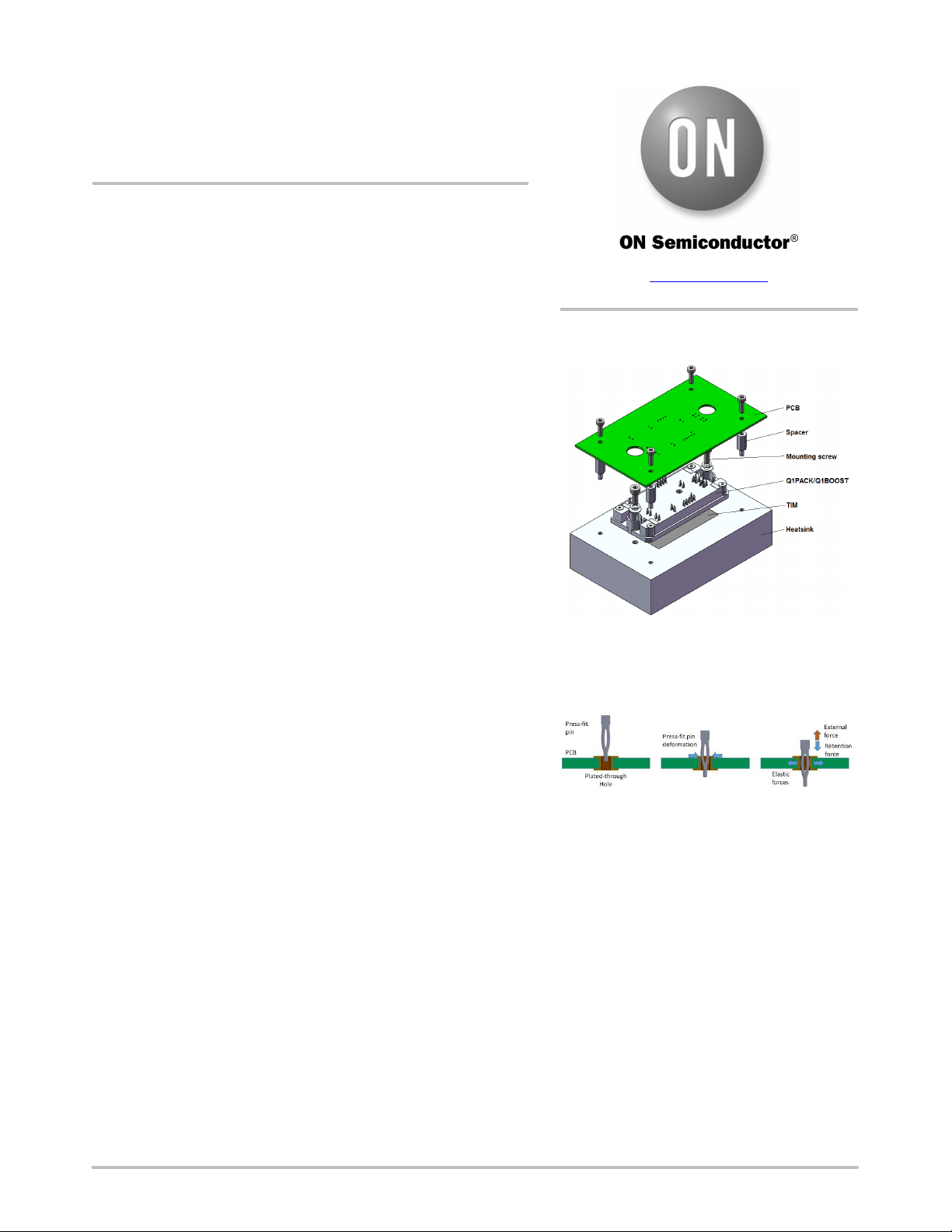
ON Semiconductor family of Power Integrated Modules has
package options using solder pins or press−fit pins for the connection
of the module to a Printed Circuit Board (PCB). Figure 1 shows a Q1
module with press−fit pins as an example.
After mounting, press−fit pins provide a cold−welding connection
between pins and plated through holes (PTH) of the PCB. This easy
assembly method avoids extra heating, avoids contamination and
provides good mechanical and electrical performance. Press−fit
assembly is a well−established connection method for power
semiconductor modules. The press−fit pins provide a gas−tight metal
to metal contact between the press−fit pin and the plated through hole
(Figure 2).
Modules having solder pins are soldered into the PCB. Modules
having press−fit pins can also be soldered into the PCB, but with larger
holes than used for the standard press−fit process.
The purpose of this application note is to provide recommendations
for the PCB and to recommend mounting and dismounting methods
with proper tools to achieve the required reliability and performance
with either press−fit or solder connections.
Figure 1. Q1 Module with PCB and
Heatsink
Figure 2. Press−fit Process
© Semiconductor Components Industries, LLC, 2019
January, 2021 − Rev. 2
1 Publication Order Number:
AND9867/D
Page 2
AND9867/D
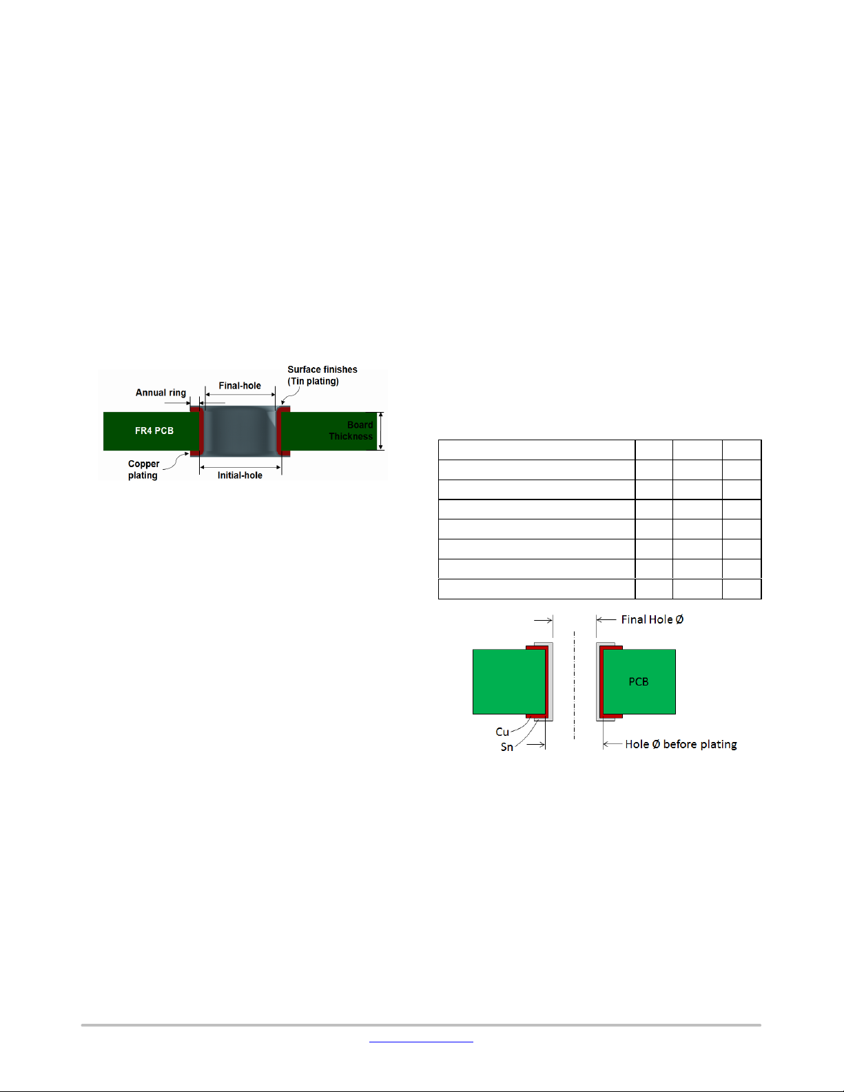
PCB SPECIFICATION
Correct design of the plated through holes (PTH) in the
PCB is essential to obtain good quality press−fit or solder
connections.
PCB Specification
The schematic structure of a plated through hole is shown
in Figure 3. If the initial drilled hole diameter is too small,
the press−in force into the PTH will be too high and
mechanical damage on both press−fit pin and PTH will
occur. If the final hole diameter is too small, damage to the
pin and the hole may also occur. If the final hole diameter is
too large, it may not provide a reliable connection between
plated through hole and press−fit pin.
The effect of the pad size in reducing the creepage and
clearance between pins should always be considered in
minimum permissible spacing calculations.
Figure 3. Cross−section of PCB
Tables 1−4 list the recommended PCB specification based
on the evaluation of the press−fit technology according to
the IEC 60352−5 standard.
Specification for Modules with Press−fit Pins,
Soldered to the PCB
It is not recommended that press−fins are just soldered
without being pressed into the PCB in mass production. If
modules with press−fit pins are reused after being removed
from the PCB, it can be soldered on the PCB to reinforce the
contact.
The pcb pad diameter is determined by the minimum
annular ring size, the production alignment tolerance (level
A, B or C) and the drilling tolerance as detailed in IPC−2222.
The effect of the pad size in reducing the creepage and
clearance between pins should always be considered in
minimum permissible spacing calculations.
Specification for Modules with Solder Pins,
Soldered to the PCB
The recommended final PCB hole diameter for solder pins
is 1.2 mm when using 1 mm pins used in F1, F2, Q0, Q1 and
Q2 modules.
The pcb pad diameter is determined by the minimum
annular ring size, the production alignment tolerance (level
A, B or C) and the drilling tolerance as detailed in IPC−2222.
The effect of the pad size in reducing the creepage and
clearance between pins should always be considered in
minimum permissible spacing calculations.
For 1 mm diameter pin, the final pad diameter for level B
manufacturing is calculated as 1.8 mm: allowing for 50 mm
absolute minimum annular ring, 0.5 mm alignment
tolerance and 1.2 mm actual PCB hole size.
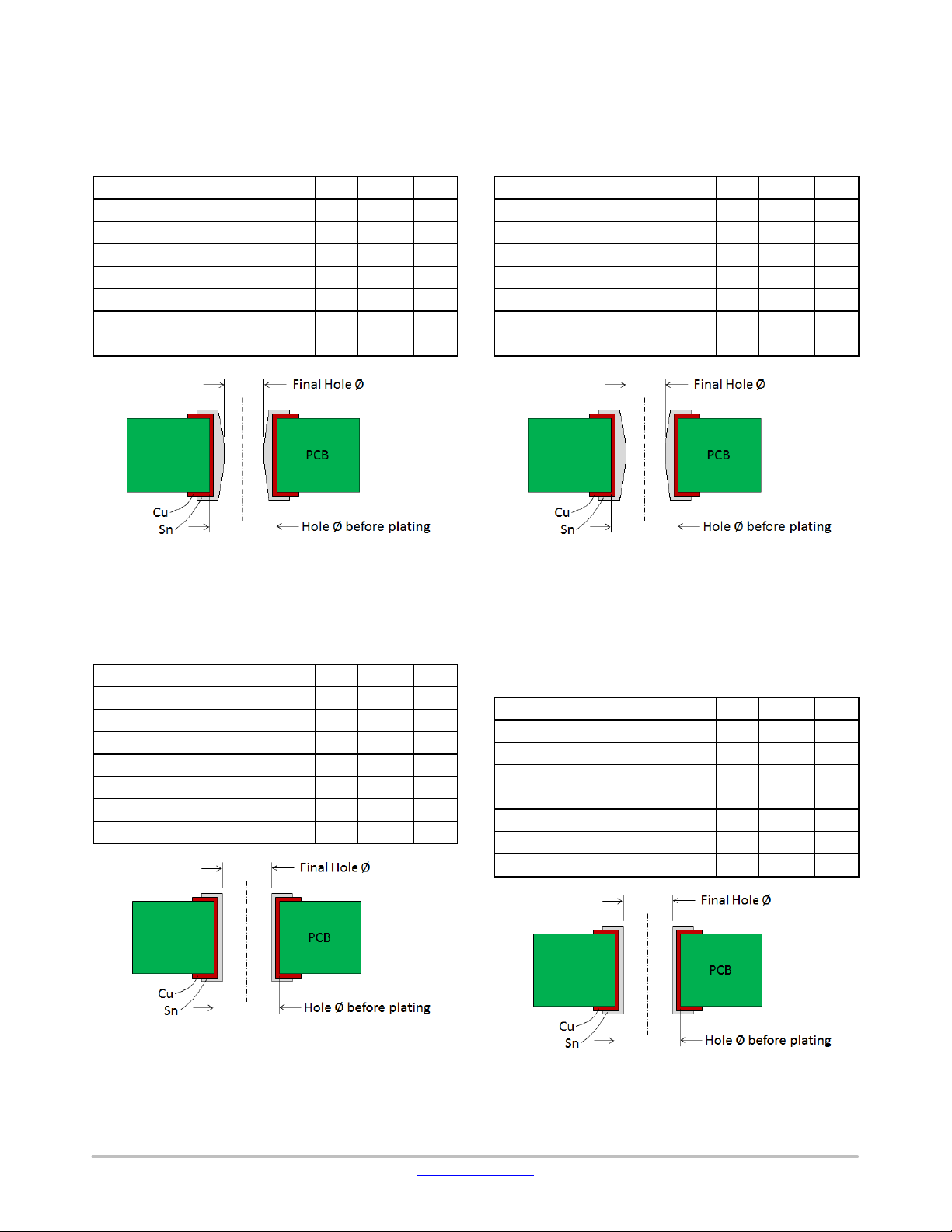
Table 1. PCB SPECIFICATIONS FOR F1 AND F2
MODULES WITH 1.2 MM PRESS−FIT PINS −
IMMERSION OR GALVANIC TIN. Pins are IEC qualified for
immersion tin plating.
Min. Typ. Max.
Initial Drilled Hole Diameter Ø [mm] 1.12 1.15
Cu Thickness in the Hole [mm]
Sn Thickness [mm] (Chemical Tin)
Final Hole Ø [mm] 0.98 1.09
Annular ring [mm]
Thickness of Conductive Layer [mm]
Board Thickness [mm] 1.6
Figure 4.
25 50
15
200
35 70−105 400
www.onsemi.com
2
Page 3
AND9867/D
Table 2. PCB SPECIFICATIONS FOR F1 AND F2
MODULES WITH 1.2 MM PRESS−FIT PINS − HAL
PLATING.
immersion/galvanic tin is recommended for more consistent
mounting.
Initial (Drill) Hole Ø [mm] 1.12 1.15
Cu Thickness in the Hole [mm]
Sn Thickness [mm]
Final Hole Ø [mm] 0.94 1.09
Annular ring [mm]
Thickness of Conductive Layer [mm]
Board Thickness [mm] 1.6
Pins are IEC qualified for HAL plating but
Min. Typ. Max.
25 50
40
200
35 70−105 400
Table 4. PCB SPECIFICATIONS FOR Q0, Q1 AND Q2
MODULES WITH 1.6 MM PRESS−FIT PINS − HAL
PLATING.
immersion/galvanic tin is recommended for more consistent
mounting.
Initial (Drill) Hole Ø [mm] 1.57 1.60
Cu Thickness in the Hole [mm]
Sn Thickness [mm]
Final Hole Ø [mm] 1.41 1.56
Annular ring [mm]
Thickness of Conductive Layer [mm]
Board Thickness [mm] 1.6
Pins are IEC qualified for HAL plating but
Min. Typ. Max.
25 50
40
200
35 70−105 400
Figure 5.
Table 3. PCB SPECIFICATIONS FOR Q0, Q1 AND Q2
MODULES WITH 1.6 MM PRESS−FIT PINS −
IMMERSION OR GALVANIC TIN.
immersion tin plating.
Initial Drilled Hole Diameter Ø [mm] 1.57 1.60
Cu Thickness in the Hole [mm]
Sn Thickness [mm] (Chemical Tin)
Final Hole Ø [mm] 1.41 1.56
Annular ring [mm]
Thickness of Conductive Layer [mm]
Board Thickness [mm] 1.6
Pins are IEC qualified for
Min. Typ. Max.
25 50
15
200
35 70−105 400
Figure 7.
Table 5. PCB SPECIFICATIONS FOR F2 MODULES
WITH EON PRESS−FIT PINS − IMMERSION OR
GALVANIC TIN.
plating. For HAL tin coating, a thicker tin thickness of up to
40 um is permitted reducing the hole size to 0.94 mm but this
requires additional approval from ON Semiconductor.
Initial Drilled Hole Diameter Ø [mm] 1.12 1.15
Cu Thickness in the Hole [mm]
Sn Thickness [mm] (Chemical Tin)
Final Hole Ø [mm] 1.02 1.09
Annular ring [mm]
Thickness of Conductive Layer [mm]
Board Thickness [mm] 1.6
Pins are IEC qualified for immersion tin
Min. Typ. Max.
25 50
15
200
35 70−105 400
Figure 6.
Figure 8.
www.onsemi.com
3
Page 4

AND9867/D
PCB DESIGN
PCB Layout Restrictions
PCB bending during the press−in process causes
mechanical stress to other PCB components, such as
capacitors and resistors. Experiments to verify a safe
minimum distance between passive components and the
plated through hole were conducted with FR4 PCB. Various
sizes (0603, 0805, 1206, 1210, 1812, and 2220) of
mechanically sensitive components were evaluated. Based
on experimental results, the recommended minimum space
between center of the plated through hole and the edge of the
component is 4 mm, as shown in Figure 9.
Mounting with Distance of 12 mm
Option 1: without spacers
Figure 10. Mounting Height with Module as Spacer
Option 2: with spacers
Figure 11. Mounting Height with Spacer in case of
using Recommended Press−fit Tool
Example: Q1 Module with Press−fit Pins
Figure 12 shows an example of mounting a Q1 module.
The Q1 package has its power connectors/terminals
distributed across the surface of the plastic case. Electrical
connections are made by connecting these terminals to
a print circuit board (PCB) by soldering or press−fit
technology.
Figure 9. PCB Design Restriction: Distance
from Center of PTH to Edge of Components
The minimum distance between the edge of the PCB and
the centre of the pin hole must be more than 4 mm.
The minimum distance between the center of the pin hole
and a neighbored component on the PCB must be more than
4 mm.
Recommended PCB−thicknesses and Mounting
Heights by Module Type
The distance between the top surface of the heatsink and
the bottom plane of the PCB is defined by the module height
of 12 mm for Q0, Q1, F1 and F2 packages or 17 mm for Q2
packages. PCB spacers can be used for fixing. The number
and the position of the fixing points depend on the design of
the circuit, location of different masses like capacitors or
inductor and the environment of the system. General
recommendations cannot be given. The recommended
heights of these spacers are given in the following sections
Figure 12. Q1 Package Mounting Example
The PCB has four mounting holes for the spacers, two
cut−out holes for accessing the heatsink mounting screws
through the PCB and the holes for the pin connections.
The dimensions and positions of the cut−out holes, the
PTH holes and mounting holes are specified in the datasheet
drawing for the specific module.
The Q0 solder pin modules have plastic mounting clips
which require different shaped cut−outs in the PCB as
specified in the datasheet.
www.onsemi.com
4
Page 5
AND9867/D
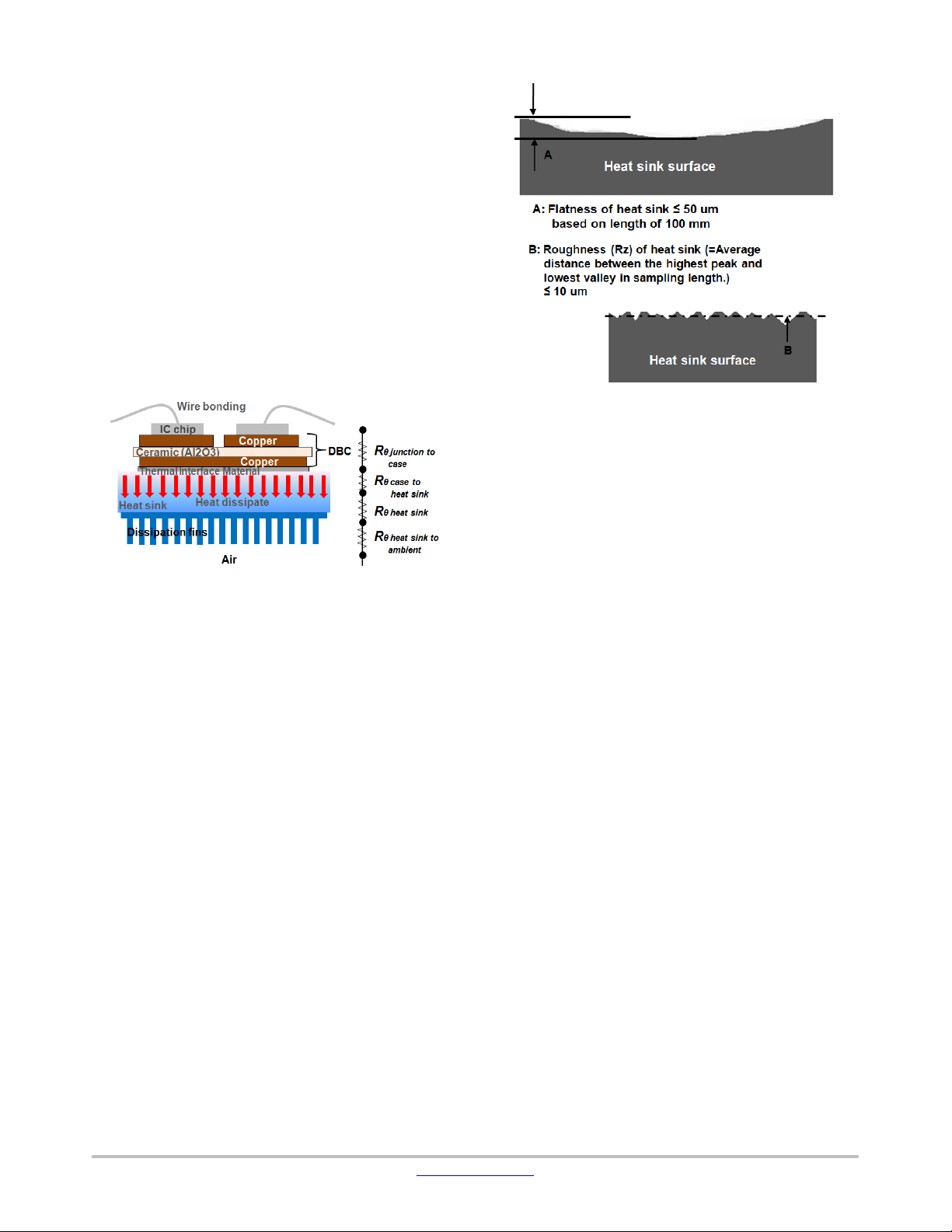
HEATSINK AND THERMAL INTERFACE
MATERIAL
Power semiconductor modules generate heat that needs to
be dissipated to protect against overheating. In general,
module operation temperature should not exceed the
maximum allowable junction temperature (T
in the datasheet. Thermally conductive metal heatsinks that
absorb and disperse heat are commonly used for cooling
high power electronics. The thermal performance of
a module, in combination with a heatsink, can be
characterized by the thermal resistance R
sum of all thermal resistances in the thermal path:
junction−to−case (R
), and heatsink−to−ambient (R
(R
sink
q
), case−to−heatsink (R
jc
q
sa
q
Figure 13.
) specified
Jmax
, which is the
ja
q
), heatsink
cs
q
), as shown in
Figure 14. Microscopic View of Surfaces.
A is Flatness and B is Roughness (Rz)
The interface surface of the heatsink must be free of
particles and contamination. Avoid handling the heatsink
surface with bare hands or contacting any foreign materials.
If it is necessary to remove contamination from heatsink,
cleaning can be accomplished using dry cloth soaked with
solvent, such as isopropyl or ethylene alcohol.
Figure 13. Thermal Model of Power Module &
Heatsink
Generally, air convection is the dominant heat transfer
mechanism in electronics. The heat transfer by air
convection strongly depends on the air velocity and the area
of the heat−transferring surface. Proper contact between
module substrate and the surface of the heatsink is crucial for
managing the overall thermal efficiency of the system.
Thermal Interface Materials (TIMs) are thermally
conductive materials used to achieve good mating of the two
surfaces and improve heat transfer.
Heatsink Surface
The contact surface of a heatsink must be flat and clean to
maximize heat transfer. Rough surfaces result in large voids
between the substrate of the module and the surface of the
heatsink. The following surface qualities are required for the
heatsink to achieve a good thermal conductivity, according
to DIN 4768−1. Roughness (Rz) should be 10 mm or less and
flatness, based on a length of 100 mm, should be 50 mm or
less. The heatsink should have no contamination,
unevenness, and burrs on the surface contacting the module.
Thermal Interface Material (TIM)
The backside of the module and the surface of the heatsink
are not ideally smooth. TIM is used to prevent air cavities
and help the thermal dissipation. Such TIM material may be
a thermal pad, foil, grease, or any other similar material. The
material selection should consider the thermal conductivity,
drying out behavior during aging, and shape maintaining
properties during power ON/OFF cycling.
The surfaces of the heatsink and the substrate of the
module are not perfectly flat. After the module is mounted
to a heatsink, air gaps can form between these two surfaces
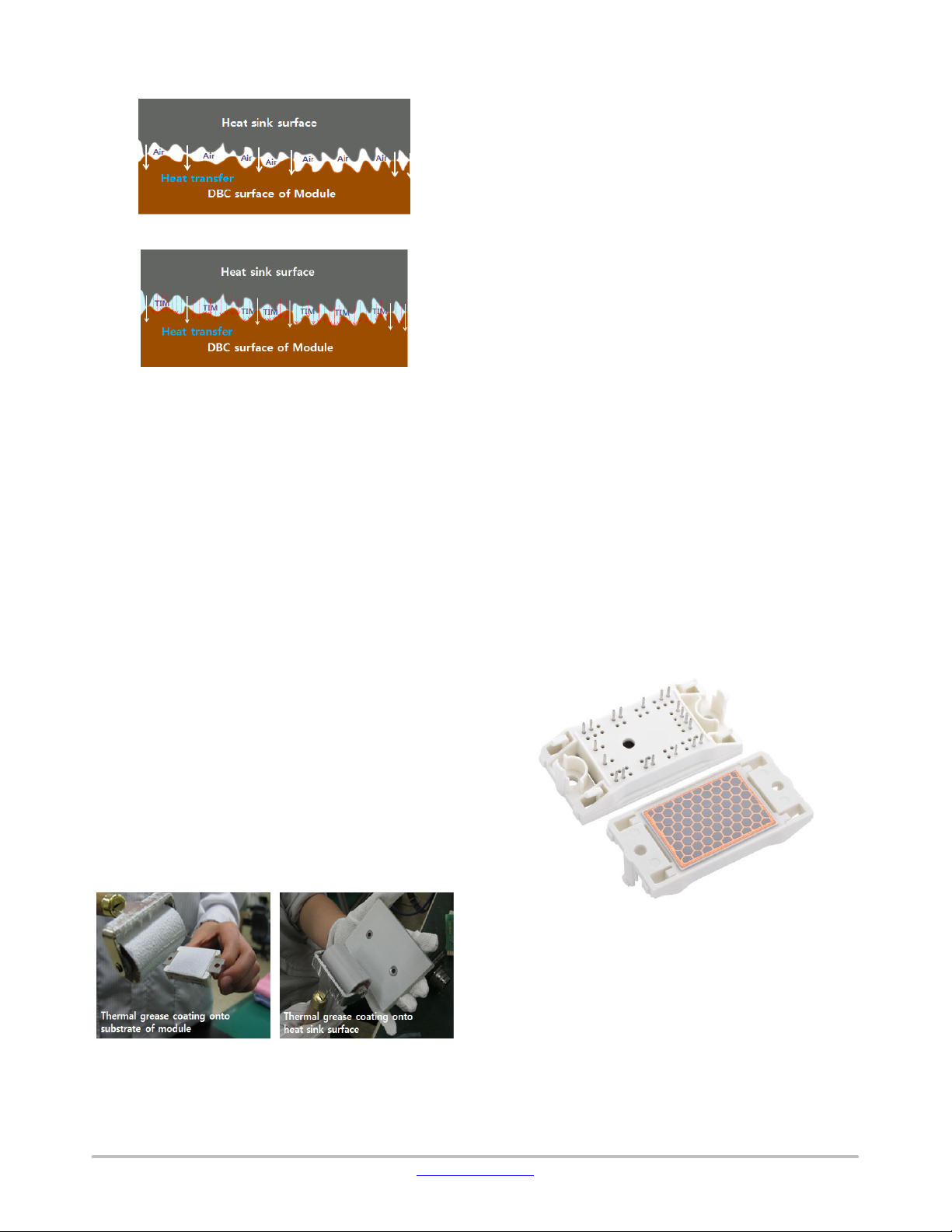
and the effective contact is limited to the area shown in
Figure 15. Air is a poor heat conductor with 0.03 W/m⋅K
thermal conductivity. It acts as a thermal barrier that limits
the efficiency of heat transfer from the device.
www.onsemi.com
5
Page 6
AND9867/D
(a)
(b)
Figure 15. (a) Heat Transfer, Module to Heatsink,
(b) Heat Transfer with Thermal Interface Material
Thermal interface materials are widely used in the
industry to fill air gaps between contact surfaces. Thermal
interface material provides better thermal performance than
air and compensates for imperfect mating surfaces, such as
roughness and flatness shown in Figure 14. There are
various thermal interface materials available in the market.
The right choice of material is an essential factor for the
application. It should be selected considering the following
features:
• High Thermal Conductivity
• Ease of Distribution with Low Contact Pressure
• Minimal Thickness
• Degradation of Characteristics Over Time
• Stability of Characteristics Over Time
• Toxicity (Non−Toxic Optimal)
• Ease in Handling during Application or Removal
1. Choose one side of the surface, module substrate,
or heatsink to apply thermal grease.
2. Coat a rubber roller with thermal grease.
3. Paint the surface repeatedly using the rubber roller
to create a uniform layer of thermal grease around
80–100 mm thick.
Since the thermal grease has the lowest thermal
conductivity in the thermal path, a layer as thin as possible
is necessary to keep the overall thermal resistance low.
Recommended thickness of printing layer is 60–100 mm to
fill the gap between two contact surfaces completely. Check
the thermal grease thickness with thickness gauges, such as
wet film combs or wet film wheels. Because manual control
of the printing pressure and speed can be learned by
experience, training is needed to achieve a technique for
good quality printing layer in real application.
Alternatively, apply thermal paste by screen printing, for
example using a honeycomb pattern. The recommended
thermal paste thickness is 80−100 mm A thickness of the
TIM layer in excess of this recommendation will
unnecessarily increase thermal resistance.
When applying thermal grease, the material must be
applied uniformly on the whole surface which is in contact
to the module substrate surface. If the module is
re−mounted, surfaces should be cleaned and TIM needs be
applied again.
Pre−applied Thermal Interface Material
As an option the module may be prepared or provided with
a pre−applied PCM layer. The recommended pattern for
such PCM layer is shown in Figure 17.
Thermal Grease
The most common thermal interface materials are thermal
greases. Thermal grease can be applied to the heatsink or the
module substrate using a rubber roller or spatula or by screen
printing. A rubber roller, as shown in Figure 16, is an easy
and fast method for applying thermal grease.
Figure 16. Applying Thermal Grease
www.onsemi.com
Figure 17. Printing Pattern Example for TIM Material
Modules Shipped with Pre−applied Phase−change
Material
Please refer to the application note referring to handling
modules with pre−applied TIM material.
6
Page 7

AND9867/D
PRESS IN PROCESS OF MODULES WITH
PRESS−FIT PINS
The press−fit process is a cost−effective way to assemble
power modules without introducing additional thermal
stress. The press−fit connection generates a good electrical,
and also strong mechanical connection between the module
and the PCB. This section deals with the mounting process
to achieve suitable press−fit connections.
There are several types of presses available; from simple
toggle presses to the automated pneumatic presses shown in
Figure 18. If possible, monitor the press−in/press−out
distance, speed, and force to achieve mechanical stability
and high reliability of the press−fit connection. The travel
distance during the press−in process should be controlled to
ensure that the press−fit zone of the pins sits properly in the
plated through hole. The speed also influences the quality of
the press−fit connection; therefore, speed recommended by
IEC standard should be applied.
Figure 19. Recommended Tooling Construction for
the Press−in Process
Figure 18. Press−in Presses
Generally, a module can be pressed in until the stand−offs
on the four corners of the module touch the PCB. If, for
example, more than one module is mounted on a PCB at
short distances or assemblies are subjected to mechanical
shocks in the application, the press−in method as described
in Figure 23 is recommended.
Press−in Tool Construction
The preferred method is to press the module into the PCB
from the top. Pressing multiple modules into one PCB can
be done one by one; or all at once.
Pressing multiple modules at the same time requires
a press−in tool according to the above detailed single tool.
The tool has to ensure the correct leveling of the modules
and the PCB to avoid any mechanical stress.
Figure 20. Press−in Tools Closed,
Module is Pressed in
Press−in Process Parameters
The total press−in force is the result of the number of pins
in a module, multiplied with the force required for a single
pin. Press−in forces lower than 60 N/pin mean that press−fit
pin may have a less secure connection in the plated through
hole. The primary reason for the low press−fit force is that
the diameter of plated through hole is too large for the
press−fit pins. Press−in forces higher than 150 N/pin can
cause mechanical damage to the press−fit terminal, the PTH,
or to the tracks on the PCB. The recommended press−in
speed ranges from 25 mm/min to 50 mm/min in accordance
with the recommendations in IEC 60352−5.
www.onsemi.com
7
Page 8

AND9867/D
The press−fit pins have to be pressed into the holes of the
PCB to the correct depth. The center of the press−fit zone has
to be at least 0.5 mm below the top surface and at least
0.5 mm above the bottom surface of the PCB (Figure 21).
Figure 21. Press−in Depth in PCB
General Press−in Process
Figure 22 shows the general sequence of the press−in
procedure. The press−in tool is comprised of two parts: the
upper press−in tool is flat to contact with the module
backside evenly and the lower press−in tool has engraved
spaces to accommodate the press−fit pins.
The two parts of the tool need to be aligned to each other
(a). In the first step of the assembly, the printed circuit board
is placed on the alignment pins of the lower part of the
press−in tool (b).
Then, the module is placed on top of the printed circuit
board using the alignment pins. It is necessary to check if the
module and the printed circuit board are in alignment (c). In
the next step, the press−in force is applied via the upper part
of the press−in tool to the backside of the module evenly. The
module should be pressed−in with a speed of
25~50 mm/min until the stand−offs on the four corners of
the module touch the surface of the printed circuit board
while press−in distance and force are monitored at the same
time (d).
It is required to adjust the traveling distance of the press
to avoid damages to the module case due to pressure being
applied. A simple manual press does not use a distance
sensing system, so a distance keeper should be designed on
the press−in tool to terminate press−in process
appropriately. The next section describes the function of the
distance keeper more in detail.
Figure 22. Press−in Process
www.onsemi.com
8
Page 9

AND9867/D
Press−in Process for Multiple Modules
In case multiple modules are assembled to the same PCB
and heatsink, height tolerances can result in unintended
bending of the PCB or inappropriate heatsink contact.
Therefore, if more than one module is mounted on the
same PCB, it is required to minimize the height tolerances
between those modules. This section presents a modified
press−in process related to that.
Figure 23 shows a press−in tool including distance
keepers. The distance keeper terminates the press−in
process and limits the press−in depth.
By contacting the printed circuit board ahead of the
module case, it prevents direct contact between the case and
the PCB. If the distance keeper contacts the surface, press−in
force rises sharply and the press−in process can be
terminated by reaching the limit of the press−in force. The
distance keeper should be designed to avoid the collision
with other PCB components.
The press−in process using the distance keeper is
described in Figure 23. First, the PCB should be placed on
the lower press−in tool (a). Then, a module is placed on the
lower press−in tool and aligned with the PCB (b). The
press−in stroke is applied to the backside of the module until
the distance keeper touches the surface of the PCB (c).
Figure 23. Press−in Process with Distance Keepers
Figure 24. Schematic Description of the Press−in Process using Distance Keeper
www.onsemi.com
9
Page 10

AND9867/D
As illustrated in Figure 25, depending on the length of the
distance keeper, the contact length between press−fit pins
and the plated through hole is determined. The total height
of the module is 12.00 ±0.30 mm for Q0, Q1, F1 and F2
modules. It is recommended that the length of the distance
keeper should be 12.40 (+0.05/−0) mm to achieve a stable
contact length.
A: Package height (DBC bottom to case top) is 12.00 +0.30/−0.30 (mm)
B: Distance keeper height is 12.40+0.05/−0
C: Air gap between case top and surface of the PCB
Figure 25. Press−in Depth in Accordance with Length of Distance Keeper
Press−in Tool Design Comments
Some design options should be considered to avoid
press−in failure. First, the contact plate of the upper press−in
tool must be larger than the module DBC substrate size. If
the contact area of the upper press−in tool is smaller than the
module substrate and pressure is applied to the center area
of the module only, the module can be mechanically
damaged during the press−in process. The press−in tool
design should consider the size of the module.
If other components (capacitors, resistors) are assembled
on the PCB next to the module mounting area, the press−in
tool design should avoid collision during the press−in
process. As shown in Figure 20, the lower press−in tool is
designed with engraved spaces for the press−fit pin and other
PCB Based on experimental results, components did not
exhibit mechanical or electrical damages due to board
bending during the press−in process when the distance
between the center of the plated through hole and the edge
Consequently, an air gap between the top of the case and
the surface of the PCB remains. Screwing the PCB down to
the stand−offs of the module case, as shown in Section 5, is
not allowable. Instead, the assembly should use space posts
to support the PCB.
(mm)
of the component is 4 mm or more. It is also important to
keep a certain area to provide support for the PCB.
Press−out Process
In some situations, it is necessary to remove power
modules from the PCB. It is possible to disconnect the
contact between module pins and PTH. The press−out
process can be performed with the same equipment used in
the press−in process.
Careful handling in the press−out process is essential to
avoid mechanical damage to both the module and the PCB.
PCB can be re−used once with a new module.
Please note: in case a module which was pressed out of a
PCB should be used again, it is necessary to solder the
module to the PCB; this is because the press−fit zone will
remain deformed after the press−out process. An additional
press−in cycle will result in low holding forces between the
press−fit pin and PCB hole.
www.onsemi.com
10
Page 11

AND9867/D
Figure 26. Press−out Tools
Figure 27. Press−out Process
The press−out tool consists of an upper and a lower
press−out tool, as shown in Figure 26. The upper press−out
tool should be parallel and aligned to the lower press−out
tool (a). The assembled board should be placed on the lower
press−in tool (b). The upper press−out tool moves down and
contacts the projecting part of the pins. Press−out force
should be applied to all pins evenly within 3−12 mm/min of
press−out speed according to IEC 60352−5 (c). The module
falls down to the lower tool as it is disassembled from the
PCB. The press−out distance should be monitored to ensure
the upper press−out tool does not apply unnecessary
pressure on the PCB after the module is fully pressed−out
(d).
Press−out Tool Design
The upper and lower press−out tools should be parallel to
each other to prevent stress on the module during press−out
process. Some pins may have contact with the upper
press−out tool while other pins have no contact with tool.
Pulling force can be exerted on the press−fit pins where
upper the press−out tool does not contact.
The press−out tool design should consider other
components assembled on the PCB next to the module
mounting area to avoid collision during the press−out
process. The specific tool to disassemble the modules from
the PCBs has two parts similar to the press−in tool. The
lower part serves as a support for the PCB. It has a cavity and
supporting pins. It is important that the size of the cavity is
close to the dimensions of the module. The supporting pins
are in line with the fixing pins of the upper part. There may
be components mounted to the PCB in the area of the tool,
in such case it is possible to cut out the nest.
The upper part consists of two pressing plates that are
connected by springs. The pins on the lower plate serve to
fix the PCB. With the aid of these parts, the bending of the
PCB can be prevented during pressing.
The ram fastened to the upper plate is designed according
to the positions of the parts on the PCB and the layout of the
pins.
It is not possible to press the module out with a flat plate
if the PCB is thicker than 2.5 mm due to the overhang of the
pins. In this case, pressing sticks positioned according to the
pin layout are necessary.
Recommended spring force: 25 N/mm
Recommended number of springs: 4 pcs
www.onsemi.com
11
Page 12

AND9867/D
Figure 28. Press−out Failure Mode: Upper and Lower
Press−out Tools Not Parallel
Due to the stress relaxation between contact partners, the
initial contact force tends to reduce over time. In addition,
the press−out force varies in relation to the contact ratio
between press−fit pin and plated through hole. As shown in
Table 6, the press−out force should be higher than 40 N per
pin.
Table 6. PRESS−OUT FORCE AND SPEED
SPECIFICATION
Min. Typ. Max.
Press−Out Force (per Pin) 40 N
Press−Out Speed 3–12 mm/min
This condition is automatically fulfilled with the use of the
recommended press−in tool.
SOLDERING TO PCB
PCB holes with fully plated through−holes will enable
100% wetting and fillets between pin and both sides of PCB.
Figure 29. Solder Wetting of PCB Through Hole
Figure 30. Wave Solder Profile
MODULE MOUNTING TO HEATSINK
This section describes how the modules are mounted to
the heatsink. The different module family members have
different sized mounting holes and recommendations.
It is extremely important that the contact surface of
heatsink must be flat and free of particles. Avoid handling
the heatsink surface with bare hands or contacting with any
foreign materials. If it is necessary to remove
contaminations from heatsink, please clean it using a dry
cloth soaked with solvent such as isopropyl or ethylene
alcohol.
Methods of Screw Clamping
There are two recommended screw clamping methods
which apply to all modules. The F1 module is used as an
example. Figure 31 describes one method for fastening the
module to the heatsink. Fasten two screws simultaneously to
prevent tilting or rising of one side of module during
fastening. Electric screwdrivers can tighten the screws with
the specified torque. Additional flat or spring washers are
permissible, considering clearance and creepage distances
specified later in this section.
Screw holes on heatsink need to be countersunk.
If method 1 cannot be applied, the method as described in
Figure 32 is also acceptable. Fasten the first screw loosely
to prevent tilting or rising of the module (step 1). Then insert
the second screw with final torque so as to be fully tightened
with the heatsink (step 2). Finally, apply full torque to the
first screw for solid tightening with the heatsink.
For F1/F2 packages in full plastic cases, the
recommended torque is between 1.6−2.0 Nm using M4
screws.
Wave soldering profile
www.onsemi.com
12
Page 13

AND9867/D
Mtorque
1.6−2.0 Nm
Mtorque
1.6−2.0 Nm
Figure 31. Illustration of Screw Clamping with Heatsink (Method 1)
Torque Values Apply to F1/F2 Packages. See Later Diagrams for Other Packages
Mtorque
1.6−2.0 Nm
Mtorque
1.6−2.0 Nm
Figure 32. Screw Clamping Steps (Method 2)
Torque Values Apply to F1/F2 Packages. See Later Diagrams for Other Packages
Q0/Q1 Modules
When using screws with flat washers:
Metric screw: M4 (recommended screw type DIN7984)
Flat washer: D = 8 mm ISO 7092 (DIN 433)
Spring washer: D = 8 mm DIN 127 or DIN 128
Mounting torque: 1.6−2.0 Nm
Screw holes on heatsink need to be countersunk.
A torque wrench shall be used to tighten the mounting
screws at the specified torque. Excessive torque may result
in damage or degradation of the device. The inaccuracy of
torque wrench tightening method can range up to ±12%.
This has to be taken into account to prevent over−tightening
the fastener.
Due to excessive temperature fluctuations washers should
be used to prevent the loosening of the screws. After
accurate tightening of the screws the spring washer exerts
a constant force on the joint. The flat washer distributes this
force on the plastic surface.
When using screws with pre−assembled washers:
Screws with pre−assembled washers (SEMS or kombi
screws) combine the screw and the washers into a single
component. These screws eliminate the need to slip the
www.onsemi.com
13
Page 14

AND9867/D
washers into place by hand, boosting the speed and
efficiency of the assembly process. The specifications of
these screws are provided below:
Screw size: M4 according to DIN 6900 (ISO 10644;
JIS B1188)
Flat washer: According to DIN 6902 Type C (ISO 10673
Type S; JIS B1256)
Washer outer diameter:
8 mm diameter can be fitted onto the module
Split lock spring washer:
According to DIN 6905(JIS B1251)
Mounting torque range: 1.6−2.0 Nm
See Figure 33.
Step 2: pre−mount
with 0.4−0.6N.M
Step 1: pre−mount
with 0.4−0.6N.M
Step 4: mount with
1.6−2N.M
Figure 33. Q0/Q1 Modules − Mounting to Heatsink
Step 3: mount with
1.6−2N.M
MOUNTING HEATSINK AND MODULE TO PCB
Mounting screws for attaching module to PCB
Screwing the PCB to the stand−offs on the module is one
of the assembly methods. By adding this screw connection
to the stand−offs, securing the assembly of module and PCB
can be expected. Figure 35 shows the key dimensions of the
stand−off. Self−tapping screws are recommended so that the
screws form the thread in the hole.
For F1 and F2 modules, metric screws, self−tapping, with
dimensions of 2.5xL or 2.6xL have been verified. The length
of the screws (L) may differ depending on the thickness of
the PCB. Typically, an 8 mm long screw (M2.5X8) can be
used with 1.6 mm−thick PCB. Recommended mounting
torque is 0.4~0.5 Nm for each screw. See Figure 30. This
shows the recommended sequence for mounting the PCB to
the module. Straight inserting avoids mechanical damage to
the module case. An electric screwdriver helps achieve
uniform force and speed for inserting the screws.
For Q2 modules, metric screws, self−tapping, with
dimensions of 2.5xL have been verified. The length of the
screws (L) may differ depending on the thickness of the
PCB. Typically, an 8 mm long screw (M2.5X8) can be used
with 1.6 mm−thick PCB. Recommended mounting torque is
0.3~0.5 Nm for each screw. See Figure 36. This shows the
recommended sequence for mounting the PCB to the
module. Straight inserting avoids mechanical damage to the
module case. An electric screwdriver helps achieve uniform
force and speed for inserting the screws.
Q0 and Q1 modules do not have screw holes for mounting
onto the PCB.
Q2 Modules
Use M5 screws with torque of 3.0–5.0 Nm.
See Figure 34.
Figure 34. Q2 Modules − Mounting to Heatsink
www.onsemi.com
14
Page 15

AND9867/D
Figure 35. Q2 Screw Clamping on Stand−offs and Key Dimensions of Screw Hole
NOTE: Do not screw the PCB down to the stand−offs of
the module if an air gap remains between case
top and PCB after press−in. This can lead to
deformation of the PCB or other mechanical
damage.
Assembly of the PCB and Heatsink
The overall structure of the mounted module should be
considered.
If the PCB is large and heavy with other components
assembled to it, there is some risk the PCB can bend, creating
mechanical stress to the module and the PCB. When
www.onsemi.com
multiple modules are applied to the same PCB, height
tolerance between modules can result in the mechanical
stresses on the board and modules. To reduce stress, space
posts should be added on the heatsink, as illustrated in to
prevent movement of the PCB.
The recommended height of the space posts is 12.4
(+0/−0.1) mm. The effective distance between center of
stand−off and the space post (= X) is 50 mm minimum. If
distance keepers are used during the press−in process,
resulting in tighter height tolerances; distances between the
15
Page 16

AND9867/D
stand−off of the case and the space post (= X) smaller than
50 mm can be used.
Figure 36 shows the assembly procedure when space
posts are used and the overall assembly structure:
Modules are first pressed into the PCB following the
recommendations introduced in Section “Heatsink Surface”
before heatsink mounting. Maintaining tight height
Figure 36. Space Posts for Assembly of PCB to Heat Sink
tolerances between module and PCB is important. Next, the
thermal interface material is applied. Then the modules and
the PCB are placed on the heatsink (a).
Then the module is mounted onto the heatsink via the
module’s metal or plastic clamp. Refer to Section “Q2
Modules” for instructions of screw clamping (b). Finally, the
PCB needs to be fixed on the space posts, as described in (c).
Figure 37. Example of Whole Assembly Process for PCB and Heatsink with Space Posts
www.onsemi.com
16
Page 17

AND9867/D
During the assembly process, a single pin is not allowed
to be drawn or pushed inwards or outwards from substrate
more than ±0.2 mm or loaded with a force greater than 35 N
(except during pressing−in of press−fit pins). The special
design of press−fit pins prevents a deformation of pins
greater than 0.1 mm during the press−in process. The tension
of the pin must not exceed ±5 N at a maximum substrate
temperature of 100 °C.
Creepage and Clearance Considerations
The spacing of the assembly between the module and PCB
must meet the clearance and creepage distance required by
the relevant standards. After F1 or F2 modules are mounted
to the PCB and heatsink, the minimum clearance is the
distance between the screw head and the bottom surface of
the PCB. The size (height) of the screw head and potential
use of an additional washer, as well as the air gap between
PCB and top side of the module, influence the creepage
distance between the screw and the PCB and the module
pins. F1 and F2 modules are mounted on the heatsink using
M4 hexagon socket head screws, according to ISO 4762.
Additional washers, according to ISO 7089, can be used.
A distance of 6.8 mm between the screw and the PCB, as
shown in Figure 38, can be maintained.
Figure 38. Distance between PCB and Screw
ON Semiconductor and are trademarks of Semiconductor Components Industries, LLC dba ON Semiconductor or its subsidiaries in the United States and/or other countries.
ON Semiconductor owns the rights to a number of patents, trademarks, copyrights, trade secrets, and other intellectual property. A listing of ON Semiconductor’s product/patent
coverage may be accessed at www.onsemi.com/site/pdf/Patent−Marking.pdf. ON Semiconductor reserves the right to make changes without further notice to any products herein.
ON Semiconductor makes no warranty, representation or guarantee regarding the suitability of its products for any particular purpose, nor does ON Semiconductor assume any liability
arising out of the application or use of any product or circuit, and specifically disclaims any and all liability, including without limitation special, consequential or incidental damages.
Buyer is responsible for its products and applications using ON Semiconductor products, including compliance with all laws, regulations and safety requirements or standards,
regardless of any support or applications information provided by ON Semiconductor. “Typical” parameters which may be provided in ON Semiconductor data sheets and/or
specifications can and do vary in different applications and actual performance may vary over time. All operating parameters, including “Typicals” must be validated for each customer
application by customer’s technical experts. ON Semiconductor does not convey any license under its patent rights nor the rights of others. ON Semiconductor products are not
designed, intended, or authorized for use as a critical component in life support systems or any FDA Class 3 medical devices or medical devices with a same or similar classification
in a foreign jurisdiction or any devices intended for implantation in the human body. Should Buyer purchase or use ON Semiconductor products for any such unintended or unauthorized
application, Buyer shall indemnify and hold ON Semiconductor and its officers, employees, subsidiaries, affiliates, and distributors harmless against all claims, costs, damages, and
expenses, and reasonable attorney fees arising out of, directly or indirectly, any claim of personal injury or death associated with such unintended or unauthorized use, even if such
claim alleges that ON Semiconductor was negligent regarding the design or manufacture of the part. ON Semiconductor is an Equal Opportunity/Affirmative Action Employer. This
literature is subject to all applicable copyright laws and is not for resale in any manner.
PUBLICATION ORDERING INFORMATION
LITERATURE FULFILLMENT:
Email Requests to: orderlit@onsemi.com
ON Semiconductor Website: www.onsemi.com
◊
TECHNICAL SUPPORT
North American Technical Support:
Voice Mail: 1 800−282−9855 Toll Free USA/Canada
Phone: 011 421 33 790 2910
www.onsemi.com
17
Europe, Middle East and Africa Technical Support:
Phone: 00421 33 790 2910
For additional information, please contact your local Sales Representative
 Loading...