

Page 1
AMIS-42770
Dual High Speed CAN
Transceiver
General Description
Controller Area Network (CAN) is a serial communication protocol,
which supports distributed real−time control and multiplexing with h igh
safety level. Typical applications of CAN−based networks can be found
in automotive and industrial environments.
The AMIS−42770 Dual−CAN transceiver is the interface between
up to two physical bus lines and the protocol controller and will be
used for serial data interchange between different electronic units at
more than one bus line. It can be used for both 12 V and 24 V systems.
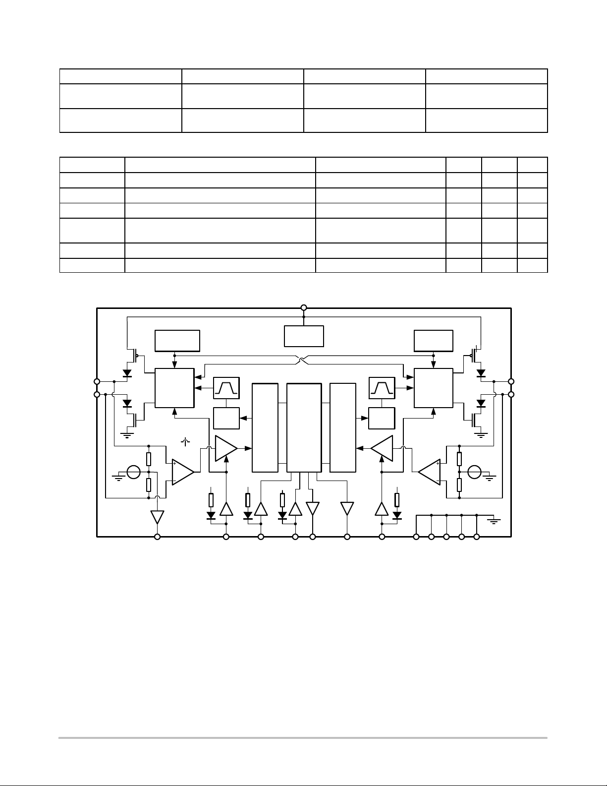
The circuit consists of following blocks:
• Two differential line transmitters
• Two differential line receivers
• Interface to the CAN protocol handler
• Interface to expand the number of CAN busses
• Logic block including repeater function and the feedback suppression
• Thermal shutdown circuit (TSD)
Due to the wide common−mode voltage range of the receiver inputs,
the AMIS−42770 is able to reach outstanding levels of electromagnetic
susceptibility (EMS). Similarly, extremely low electromagnetic
emission (EME) is achieved by the excellent matching of the output
signals.
Key Features
• Fully Compatible with the ISO 11898−2 Standard
• Certified “Authentication on CAN Transceiver Conformance (d1.1)”
• Wide Range of Bus Communication Speed (up to 1 Mbit/s in
Function of the Bus Topology)
• Allows Low Transmit Data Rate in Networks Exceeding 1 km
• Ideally Suited for 12 V and 24 V Industrial and Automotive
Applications
• Low EME: Common−mode−choke is No Longer Required
• Differential Receiver with Wide Common−mode Range (±35 V) for
High EMS
• No Disturbance of the Bus Lines with an Un−powered Node
• Prolonged Dominant Time−out Function Allowing Communication
Speeds Down to 1 kbit/s
• Thermal Protection
• Bus Pins Protected against Transients
• Short Circuit Proof to Supply Voltage and Ground
• This is a Pb−Free Device*
http://onsemi.com
SOIC 20
IC SUFFIX
CASE 751AQ
20
AMIS42770
ICAW−N
AWLYYWWG
1
A = Assembly Location
WL = Wafer Lot
YY = Year
WW = Work Week
G = Pb−Free Package
ORDERING INFORMATION
See detailed ordering and shipping information in the package
dimensions section on page 2 of this data sheet.
*For additional information on our Pb−Free strategy and soldering details, please
download the ON Semiconductor Soldering and Mounting Techniques
Reference Manual, SOLDERRM/D.
© Semiconductor Components Industries, LLC, 2014
November, 2014 − Rev. 4
1 Publication Order Number:
AMIS−42770/D
Page 2
AMIS−42770
ORDERING INFORMATION
Part Number Package Shipping Configuration Temperature Range
AMIS42770ICAW1G SOIC−20 300
(Pb−Free, Green)
AMIS42770ICAW1RG SOIC−20 300
(Pb−Free, Green)
T able 1. TECHNICAL CHARACTERISTICS
Symbol Parameter Conditions Min. Max. Unit
V
CANHx
V
CANLx
V
o(dif)(bus_dom)
CM−range Input common−mode range for comparator Guaranteed differential receiver
V
CM−peak
V
CM−step
1. The parameters V
DC voltage at pin CANH1/2 0 < VCC < 5.25 V; no time limit −45 +45 V
DC voltage at pin CANL1/2 0 < VCC < 5.25 V; no time limit −45 +45 V
Differential bus output voltage in dominant state
Common−Mode peak See Figures 10 and 11 (Note 1) −1000 +1000 mV
Common−Mode step See Figures 10 and 11 (Note 1) −250 +250 mV
CM−peak
and V
guarantee low EME.
CM−step
VCC
12
38 / Tube −40°C to 125°C
1500 / Tape & Reel −40°C to 125°C
42.5 W < RLT < 60 W
1.5 3 V
−35 +35 V
threshold and leakage current
CANH1
CANL1
13
14
V
CC/2
−
R
R
i(cm)
i(cm)
+
shutdown
8
V
REF
Thermal
Driver
control
COMP
V
CC
Timer
10
ENB1
POR
AMIS−42770
Logic
Unit
Feedback Suppression
V
CC
V
CC
3792
4
Feedback Suppression
RintTx0Text
Figure 1. Block Diagram
Timer
ENB2
2x timer
clock
Driver
control
COMP
V
CC
5 6 15 16 17
19
CANH2
18
CANL2
R
i(cm)
V
CC/2
+
−
R
i(cm)
GNDRx0
http://onsemi.com
2
Page 3
AMIS−42770
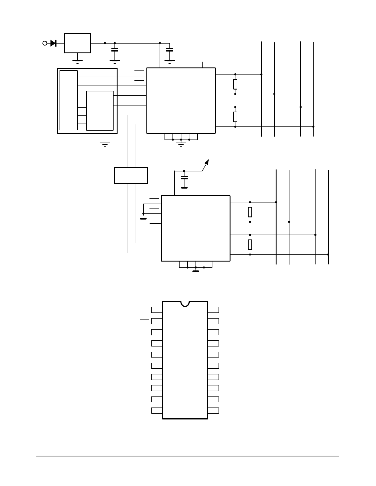
TYPICAL APPLICATION
Application Description
AMIS−42770 is especially designed to provide the link
between a CAN controller (protocol IC) and two physical
busses. It is able to operate in three different modes:
• Dual CAN
• A CAN−bus extender
• A CAN−bus repeater
Application Schematics
VBAT
5 V−reg
mC
VBAT
5 V−reg
VCC
CAN
controller
C
D
100 nF
EN1
EN2
Rx0
Tx0
Text
Rint
VCC
10
2
7
4
3
9
12
AMIS−42770
5
6 15 16 17
Vref
8
GND
13
14
19
18
CANH1
CANL1
CANH2
CANL2
R
60 W
R
60 W
Figure 2. Application Diagram CAN−bus Repeater
C
D
100 nF100 nF
AMIS−42770
5
6 15 16 17
Vref
8
GND
13
14
19
18
GND
C
D
VCC
10
12
2
7
4
3
9
EN1
EN2
Rx0
Tx0
Text
Rint
LT
LT
CANH1
CANL1
CANH2
CANL2
R
LT
60 W
R
LT
60 W
CAN BUS 2CAN BUS 1
CAN BUS 2CAN BUS 1
Figure 3. Application Diagram Dual−CAN
http://onsemi.com
3
Page 4
AMIS−42770
VBAT
5 V−reg
mC
VCC
CAN
controller
C
GND
OptoCoupler
D
Dual
EN1
EN2
Rx0
Tx0
Text
Rint
VCC
10
2
7
4
3
9
EN1
EN2
Rx0
Tx0
Text
Rint
12
AMIS−42770
5
6 15 16 17
VCC
10
2
7
4
3
9
C
D
100 nF100 nF
12
AMIS−42770
5
6 15 16 17
C
D
100 nF
Vref
8
GND
13
14
19
18
CANH1
CANL1
CANH2
CANL2
isolated +5
Vref
8
13
14
19
18
GND
R
LT
60 W
R
LT
60 W
CANH1
CANL1
CANH2
CANL2
R
LT
60 W
R
LT
60 W
CAN BUS 2CAN BUS 1
CAN BUS 4CAN BUS 3
Figure 4. Application Diagram CAN−bus Extender
NC
EN2
Text
Tx0
GND
GND
Rx0
Vref1
Rint
EN1
10
2
3
4
AMIS−42770
5
6
7
8
9
201
19
18
17
16
15
14
13
12
11
NC
CANH2
CANL2
GND
GND
GND
CANL1
CANH1
VCC
NC
Figure 5. Pin Out (top view)
http://onsemi.com
4
Page 5

AMIS−42770
Table 2. PIN DESCRIPTION
Pin Name Description
1 NC Not connected
2 ENB2 Enable input, bus system 2; internal pull−up
3 Text Multi−system transmitter Input; internal pull−up
4 Tx0 Transmitter input; internal pull−up
5 GND Ground connection (Note 2)
6 GND Ground connection (Note 2)
7 Rx0 Receiver output
8 V
9 Rint Multi−system receiver output
10 ENB1 Enable input, bus system 1; internal pull−up
11 NC Not connected
12 VCC Positive supply voltage
13 CANH1 CANH transceiver I/O bus system 1
14 CANL1 CANL transceiver I/O bus system 1
15 GND Ground connection (Note 2)
16 GND Ground connection (Note 2)
17 GND Ground connection (Note 2)
18 CANL2 CANL transceiver I/O bus system 2
19 CANH2 CANH transceiver I/O bus system 2
20 NC Not connected
2. In order to ensure the chip performance, all these pins need to be connected to GND on the PCB.
REF1
Reference voltage
FUNCTIONAL DESCRIPTION
Overall Functional Description
AMIS−42770 is specially designed to provide the link
between the protocol IC (CAN controller) and two physical
bus lines. Data interchange between those two bus lines is
realized via the logic unit inside the chip. To provide an
independent switch−off of the transceiver units for both bus
systems by a third device (e.g. the °C), enable−inputs for the
corresponding driving and receiving sections are provided.
As long as both lines are enabled, they appear as one logical
bus to all nodes connected to either of them.
The bus lines can have two logical states, dominant or
recessive. A bus is in the recessive state when the driving
sections of all transceivers connected to the bus are passive.
The differential voltage between the two wires is
approximately zero. If at least one driver is active, the bus
changes into the dominant state. This state is represented by
a differential voltage greater than a minimum threshold and
therefore by a current flow through the terminating resistors
of the bus line. The recessive state is overwritten by the
dominant state.
In case a fault (like short circuit) is present on one of the
bus lines, it remains limited to that bus line where it occurs.
Data interchange from the protocol IC to the other bus
system and on this bus system itself can be continued.
AMIS−42770 can be also used for only one bus system. If
the connections for the second bus system are simply left
open it serves as a single transceiver for an electronic unit.
For correct operation, it is necessary to terminate the open
bus by the proper termination resistor.
Logic Unit and CAN Controller Interface
The logic unit inside AMIS−42770 provides data transfer
from/to the digital interface to/from the two busses and from
one bus to the other bus. The detailed function of the logic
unit is described in Table 3.
All digital input pins, including ENBx, have an internal
pull−up resistor to ensure a recessive state when the input is
not connected o r i s a ccidentally interrupted. A d ominant s tate
on the bus line is represented by a low−level at the digital
interface; a recessive state is represented by a high−level.
Dominant state received on any bus (if enabled) causes a
dominant state on both busses, pin Rint and pin Rx0.
Dominant signal o n a ny o f the i nput p ins T x0 and T ext c auses
transmission of dominant on both bus lines (if enabled).
Digital inputs Tx0 and Text are used for connecting the
internal logic’s of several IC’s to obtain versions with more
than two bus outputs (see Figure 4). They have also a direct
logical link to pins Rx0 and Rint independently on the EN1x
pins – dominant on Tx0 is directly transferred to both Rx0
and Rint pins, dominant on T ext is only transferred to Rx0.
http://onsemi.com
5
Page 6

AMIS−42770
Transmitters
The transceiver includes two t ransmitters, one f or each bus
line, and a driver control circuit. Each transmitter is
implemented as a push and a pull driver. The drivers will be
active if t he t ransmission o f a d ominant b it i s r equired. D uring
the transmission of a r ecessive bit all drivers are passive. The
transmitters have a built−in current limiting circuit that
protects the driver stages from damage caused by accidental
short circuit to either positive supply voltage or to ground.
Additionally a thermal protection circuit is integrated.
T able 3. FUNCTION OF THE LOGIC UNIT (bold letters describe input signals)
EN1B
0 0 0 0 dominant dominant 0 0
0 0 0 1 dominant dominant 0 0
0 0 1 0 dominant dominant 0 1
0 0 1 1 recessive recessive 1 1
0 0 1 1 dominant (Note 3) dominant 0 0
0 0 1 1 dominant dominant (Note 3) 0 0
0 1 0 0 dominant recessive 0 0
0 1 0 1 dominant recessive 0 0
0 1 1 0 dominant recessive 0 1
0 1 1 1 recessive recessive 1 1
0 1 1 1 dominant (Note 3) recessive 0 0
0 1 1 1 recessive dominant (Note 3) 1 1
1 0 0 0 recessive dominant 0 0
1 0 0 1 recessive dominant 0 0
1 0 1 0 recessive dominant 0 1
1 0 1 1 recessive recessive 1 1
1 0 1 1 dominant (Note 3) recessive 1 1
1 0 1 1 recessive dominant (Note 3) 0 0
1 1 0 0 recessive recessive 0 0
1 1 0 1 recessive recessive 0 0
1 1 1 0 recessive recessive 0 1
1 1 1 1 recessive recessive 1 1
1 1 1 1 dominant (Note 3) recessive 1 1
1 1 1 1 recessive dominant (Note 3) 1 1
3. Dominant detected by the corresponding receiver.
Receivers
EN2B TX0 TEXT Bus 1 State Bus 2 State RX0 RINT
Two bus receiving sections sense the states of the bus
lines. Each receiver section consists of an input filter and a
fast and accurate comparator. The aim of the input filter is
to improve the immunity against high−frequency
disturbances and also to convert the voltage at the bus lines
CANHx and CANLx, which can vary from –12 V to +12 V,
to voltages in the range 0 to 5 V, which can be applied to the
comparators.
The output signal of the comparators is gated by the ENBx
signal. In the disabled state (ENBX = high), the output signal
of the comparator will be replaced by a permanently
The driver control circuit ensures that the drivers are
switched on and off with a controlled slope to limit EME.
The driver control circuit will control itself by the thermal
protection circuit, the timer circuit and the logic unit.
The enable signal ENBx allows the transmitter to be
switched off by a third device (e.g. the °C). In the disabled
state (ENBx = high) the corresponding transmitter behaves
as in the recessive state.
recessive state and does not depend on the bus voltage. In the
enabled state the receiver signal sent to the logic unit is
identical to the comparator output signal.
Time−out Counter
To avoid that the transceiver drives a permanent dominant
state on either of the bus lines (blocking all communication),
time−out function is implemented. Signals on pins Tx0 and
Text as well as both bus receivers are connected to the logic
unit through independent timers. If the input of the timer
stays dominant for longer than 25 ms (see parameter t
it is replaced by a recessive signal on the timer output.
dom
),
http://onsemi.com
6
Page 7

AMIS−42770
Feedback Suppression
The logic unit described in Table 3 constantly ensures that
dominant symbols on one bus line are transmitted to the
other bus line without imposing any priority on either of the
lines. This feature would lead to an “interlock” state with
permanent dominant signal transmitted to both bus lines, if
no extra measure is taken.
Therefore feedback suppression is included inside the
logic unit of the transceiver . This block masks−out reception
on that bus line, on which a dominant is actively transmitted.
The reception becomes active again only with certain delay
after the dominant transmission on this line is finished.
Power−on−Reset (POR)
While Vcc voltage is below the POR level, the POR
circuit makes sure that:
• The counters are kept in the reset mode and stable state
without current consumption
• Inputs are disabled (don’t care)
• Outputs are high impedant; only Rx0 = high−level
• Analog blocks are in power down
• Oscillator not running and in power down
• CANHx and CANLx are recessive
• VREF output high impedant for POR not released
Over Temperature Detection
A thermal protection circuit is integrated to prevent the
transceiver from damage if the junction temperature
exceeds thermal shutdown level. Because the transmitters
dissipate most of the total power, the transmitters will be
switched off only to reduce power dissipation and IC
temperature. All other IC functions continue to operate.
Fault Behavior
A fault like a short circuit is limited to that bus line where
it occurs; hence data interchange from the protocol IC to the
other bus system is not affected.
When the voltage at the bus lines is going out of the normal
operating range (−12 V to +12 V), the receiver is not allowed
to erroneously detect a dominant state.
Short Circuits
A current−limiting circuit protects the transmitter output
stage from damage caused by an accidental short−circuit to
either positive or negative supply voltage, although power
dissipation increases during this fault condition.
The pins CANHx and CANLx are protected from
automotive electrical transients (according to “ISO 7637”).
ELECTRICAL CHARACTERISTICS
Definitions
All voltages are referenced to GND. Positive currents
flow into the IC. Sinking current means that the current is
flowing into the pin. Sourcing current means that the current
is flowing out of the pin.
Table 4. ABSOLUTE MAXIMUM RATINGS
Symbol Parameter Conditions Min. Max. Unit
V
CC
V
CANHx
V
CANLx
V
digIO
V
REF
V
tran(CANHx)
V
tran(CANLx)
V
esd(CANLx/CANHx)
V
esd
Latch−up Static latch−up at all pins (Note 6) 100 mA
T
stg
T
amb
T
junc
Stresses exceeding those listed in the Maximum Ratings table may damage the device. If any of these limits are exceeded, device functionality
should not be assumed, damage may occur and reliability may be affected.
4. Applied transient waveforms in accordance with “ISO 7637 part 3”, test pulses 1, 2, 3a, and 3b (see Figure 6)
5. Standardized human body model (HBM) ESD pulses in accordance to MIL883 method 3015. Supply pin 8 is ±2 kV.
6. Static latch−up immunity: static latch−up protection level when tested according to EIA/JESD78.
7. Standardized charged device model ESD pulses when tested according to EOS/ESD DS5.3−1993.
Supply voltage −0.3 +7 V
DC voltage at pin CANH1/2 0 < VCC < 5.25 V; no time limit −45 +45 V
DC voltage at pin CANL1/2 0 < VCC < 5.25 V; no time limit −45 +45 V
DC voltage at digital IO pins (EN1B, EN2B,
Rint, Rx0, Text, Tx0)
DC voltage at pin V
Transient voltage at pin CANH1/2 (Note 4) −150 +150 V
Transient voltage at pin CANL1/2 (Note 4) −150 +150 V
ESD voltage at CANH1/2 and CANL1/2 pins (Note 5)
ESD voltage at all other pins (Note 5)
Storage temperature −55 +155 °C
Ambient temperature −40 +125 °C
Maximum junction temperature −40 +150 °C
REF
(Note 7)
(Note 7)
−0.3 VCC + 0.3 V
−0.3 VCC + 0.3 V
−4
−500
−2
−250
+4
+500
+2
+250
kV
kV
V
V
http://onsemi.com
7
Page 8

AMIS−42770
Table 5. THERMAL CHARACTERISTICS
Symbol Parameter Conditions Value Unit
R
th(vj−a)
R
th(vj−s)
DC CHARACTERISTICS
T able 6. DC AND TIMING CHARACTERISTICS
(VCC = 4.75 to 5.25 V; T
Symbol
SUPPLY (pin VCC)
I
CC
PORL_VCC Power−on−reset level on V
DIGITAL INPUTS (Tx0, Text, EN1B, EN2B)
V
IH
V
I
IH
I
IL
C
DIGITAL OUTPUTS (pin Rx0, Rint)
I
oh
I
ol
REFERENCE VOLTAGE OUTPUT (pin V
V
REF
V
REF_CM
BUS LINES (pins CANH1/2 and CANL1/2)
V
o(reces)(CANHx)
V
o(reces)(CANLx)
I
o(reces) (CANHx)
I
o(reces) (CANLx)
V
o(dom) (CANHx)
V
o(dom) (CANLx)
V
o(dif) (bus)
I
o(sc) (CANHx)
I
o(sc) (CANLx)
Thermal resistance from junction to ambient in SO20 package In free air 85 K/W
Thermal resistance from junction to substrate of bare die In free air 45 K/W
= −40 to +150°C; RLT = 60 W unless specified otherwise.)
junc
Parameter Conditions Min. Typ. Max. Unit
Supply current, no loads on digital outputs, both busses enabled
CC
High−level input voltage 0.7 x V
IL
Low−level input voltage −0.3 − 0.3 x V
High−level input current VIN = V
Dominant transmitted
Recessive transmitted
CC
45 137.5
2.2 4.7 V
CC
− V
−5 0 +5
Low−level input current VIN = 0 V −75 −200 −350
i
Input capacitance Not tested − 5 10 pF
High−level output current V
Low−level output current V
)
REF1
Reference output voltage
Reference output voltage for
full common mode range
Recessive bus voltage at pin
CANH1/2
Recessive bus voltage at pin
CANL1/2
Recessive output current at
pin CANH1/2
Recessive output current at
pin CANL1/2
Dominant output voltage at pin
CANH1/2
Dominant output voltage at pin
CANL1/2
Differential bus output voltage
(V
CANHx
− V
CANLx
)
Short circuit output current at
pin CANH1/2
Short circuit output current at
pin CANL1/2
= 0.7 x V
o
= 0.3 x V
o
−50 mA < I
−35 V <V
−35 V <V
V
= VCC; no load 2.0 2.5 3.0 V
Tx0
V
= VCC; no load 2.0 2.5 3.0 V
Tx0
−35 V < V
0 V < V
−35 V < V
0 V < V
V
V
V
= 0 V; dominant;
Tx0
42.5 W < R
V
= VCC; recessive;
TxD
V
= 0 V;V
CANHx
V
= 36 V; V
CANLx
CC
CC
< +50 mA
VREF
< +35 V;
CANHx
< +35 V
CANLx
< +35 V;
CANHx
< 5.25 V
CC
< +35 V;
CANLx
< 5.25 V
CC
= 0 V 3.0 3.6 4.25 V
Tx0
= 0 V 0. 5 1.4 1.75 V
Tx0
< 60 W
LT
no load
= 0 V −45 −70 −120 mA
Tx0
= 0 V 45 70 120 mA
Tx0
−5 −10 −15 mA
5 10 15 mA
0.45 x V
0.40 x V
CC
CC
0.50 x V
0.50 x V
CC
CC
−2.5 − +2.5 mA
−2.5 − +2.5 mA
1.5 2.25 3.0 V
−120 0 +50 mV
19.5
CC
0.55 x V
0.60 x V
CC
CC
CC
mA
V
V
mA
mA
V
V
http://onsemi.com
8
Page 9

AMIS−42770
T able 6. DC AND TIMING CHARACTERISTICS
(VCC = 4.75 to 5.25 V; T
Symbol UnitMax.Typ.Min.ConditionsParameter
BUS LINES (pins CANH1/2 and CANL1/2)
V
i(dif)(th)
V
ihcm(dif) (th)
V
i(dif) (hys)
R
i(cm)(CANHx)
R
i(cm) (CANLx)
R
i(cm)(m)
R
i(dif)
C
i(CANHx)
C
i(CANLx)
C
i(dif)
I
LI(CANHx)
I
LI(CANLx)
V
CM−peak
V
CM−step
THERMAL SHUTDOWN
T
j(sd)
TIMING CHARACTERISTICS (see Figures 8 and 9)
t
d(Tx−BUSon)
t
d(Tx−BUSoff)
t
d(BUSon−RX)
t
d(BUSoff−RX)
t
d(ENxB)
t
d(Tx−Rx)
t
dom
t
d(FBS)
Product parametric performance is indicated in the Electrical Characteristics for the listed test conditions, unless otherwise noted. Product
performance may not be indicated by the Electrical Characteristics if operated under different conditions.
= −40 to +150°C; RLT = 60 W unless specified otherwise.)
junc
Differential receiver threshold
voltage
Differential receiver threshold
voltage for high common−
mode
Differential receiver input voltage hysteresis
Common−mode input resist-
−5 V < V
−5 V < V
see Figure 7
−35 V < V
−35 V < V
see Figure 7
−35 V < V
−35 V < V
see Figure 7
CANLx
CANHx
CANLx
CANHx
CANL
CANH
< +12 V;
< +12 V;
< +35 V;
< +35 V;
< +35 V;
< +35 V;
0.5 0.7 0.9 V
0.3 0.7 1.05 V
50 70 100 mV
15 26 37
KW
ance at pin CANH1/2
Common−mode input resist-
15 26 37
KW
ance at pin CANL1/2
Matching between pin CANH1/2
and pin CANL1/2 common−
V
CANHx
= V
CANLx
−3 0 +3 %
mode input resistance
Differential input resistance 25 50 75
Input capacitance at pin
CANH1/2
Input capacitance at pin
CANL1/2
Differential input capacitance V
Input leakage current at pin
CANH1/2
Input leakage current at pin
CANL1/2
Common−mode peak during
V
= VCC; not tested 7.5 20 pF
Tx0
V
= VCC; not tested 7.5 20 pF
Tx0
= VCC; not tested 3.75 10 pF
Tx0
VCC < PORL_VCC;
−5.25 V < V
CANHx
VCC < PORL_VCC;
−5.25 V < V
CANLx
< 5.25 V
< 5.25 V
−350 170 350
−350 170 350
See Figure 11 −1000 1000 mV
KW
mA
mA
transition from dom → rec or
rec → dom
Difference in common−mode
See Figure 11 −250 250 mV
between dominant and recessive state
Shutdown junction temperature 150 °C
Delay Tx0/Text to bus active 40 85 120 ns
Delay Tx0/Text to bus inactive 30 60 115 ns
Delay bus active to Rx0/Rint 25 55 115 ns
Delay bus inactive to Rx0/Rint 65 100 145 ns
Delay from EN1B to bus act-
100 200 ns
ive/inactive
Delay from Tx0 to Rx0/Rint
15 pF on the digital output 4 10 35 ns
and from Text to Rx0
(direct logical path)
Time out counter interval 15 25 45 ms
Delay for feedback suppres-
sion release
5+
t
d(BUSon−RX)
300 ns
http://onsemi.com
9
Page 10

Measurement Set−ups and Definitions
Schematics are given for single CAN transceiver.
+5V
AMIS−42770
100 nF
Tx0
Vref
CANH1
8
13
CANL1
14
CANH2
19
CANL2
18
6151617
5
GND
Text
Rint
Rx0
EN1 EN2
VCC
3
9
4
7
10
12
AMIS−42770
2
Figure 6. Test Circuit for Automotive Transients
V
RxD
Hysteresis
0,5
0,9
Figure 7. Hysteresis of the Receiver
1 nF
1 nF
V
i(dif)(hys)
Transient
Generator
High
Low
+5 V
100 nF
Vref
8
13
14
19
18
5
6151617
GND
Tx0
Text
Rint
Rx0
VCC
12
3
9
4
7
EN1 EN2
10
AMIS−42770
2
Figure 8. Test Circuit for Timing Characteristics
CANH1
CANL1
CANH2
CANL2
R
LT
60 W
R
LT
60 W
C
LT
100 pF
C
LT
100 pF
http://onsemi.com
10
Page 11

V
CANHx−BUS
V
=
DIFF
V
CANHx
− V
CANLx
Tx0
Text
5 V
0,7 V
V
CANHx
V
CANLx
CC
0,3 V
AMIS−42770
CC
dominant
+5 V
Gen
0 V
Rx0
Rint
t
d(Tx−Rx)
t
d(Tx−BUSon)
Text
Rint
Tx0
Rx0
0,9 V
0,3 V
CC
VCC
12
3
9
AMIS−42770
4
7
2
10
EN1 EN2
0,9 V
PD(H)
t
d(Tx−Rx)
t
d(Tx−BUSoff)
0,7 V
0,5 V
CC
t
t
d(BUSon−Rx)
Figure 9. Timing Diagram for AC Characteristics
100 nF
Vref
CANH1
8
13
CANL1
14
CANH2
19
CANL2
18
5
6151617
GND
6.2 kW
6.2 kW
30 W30 W
47 nF
0,3 V
10 nF
CC
Spectrum Anayzer
0,5 V
t
d(BUSoff−Rx)
Active Probe
recessive
0,7 V
CC
Figure 10. Basic Test Set−up for Electromagnetic Measurement
http://onsemi.com
11
Page 12

AMIS−42770
CANHx
CANLx
recessive
V
CM−peak
V
= 0.5*
CM
(V
CANHx
+ V
CANLx
)
V
CM−peak
Figure 11. Common−mode Voltage Peaks (see Measurement Set−up Figure 10)
Company or Product Inquiries
For more information about ON Semiconductor’s products or services visit our Web site at http://www.onsemi.com.
V
CM−peak
http://onsemi.com
12
Page 13

MECHANICAL CASE OUTLINE
PACKAGE DIMENSIONS
SOIC 20 W
CASE 751AQ−01
ISSUE O
DATE 19 JUN 2008
DOCUMENT NUMBER:
DESCRIPTION:
ON Semiconductor and are trademarks of Semiconductor Components Industries, LLC dba ON Semiconductor or its subsidiaries in the United States and/or other countries.
ON Semiconductor reserves the right to make changes without further notice to any products herein. ON Semiconductor makes no warranty, representation or guarantee regarding
the suitability of its products for any particular purpose, nor does ON Semiconductor assume any liability arising out of the application or use of any product or circuit, and specifically
disclaims any and all liability, including without limitation special, consequential or incidental damages. ON Semiconductor does not convey any license under its patent rights nor the
rights of others.
© Semiconductor Components Industries, LLC, 2019
98AON30891E
SOIC 20 W
Electronic versions are uncontrolled except when accessed directly from the Document Repository.
Printed versions are uncontrolled except when stamped “CONTROLLED COPY” in red.
PAGE 1 OF 1
www.onsemi.com
Page 14

ON Semiconductor and are trademarks of Semiconductor Components Industries, LLC dba ON Semiconductor or its subsidiaries in the United States and/or other countries.
ON Semiconductor owns the rights to a number of patents, trademarks, copyrights, trade secrets, and other intellectual property. A listing of ON Semiconductor’s product/patent
coverage may be accessed at www.onsemi.com/site/pdf/Patent−Marking.pdf
ON Semiconductor makes no warranty, representation or guarantee regarding the suitability of its products for any particular purpose, nor does ON Semiconductor assume any liability
arising out of the application or use of any product or circuit, and specifically disclaims any and all liability, including without limitation special, consequential or incidental damages.
Buyer is responsible for its products and applications using ON Semiconductor products, including compliance with all laws, regulations and safety requirements or standards,
regardless of any support or applications information provided by ON Semiconductor. “Typical” parameters which may be provided in ON Semiconductor data sheets and/or
specifications can and do vary in different applications and actual performance may vary over time. All operating parameters, including “Typicals” must be validated for each customer
application by customer’s technical experts. ON Semiconductor does not convey any license under its patent rights nor the rights of others. ON Semiconductor products are not
designed, intended, or authorized for use as a critical component in life support systems or any FDA Class 3 medical devices or medical devices with a same or similar classification
in a foreign jurisdiction or any devices intended for implantation in the human body. Should Buyer purchase or use ON Semiconductor products for any such unintended or unauthorized
application, Buyer shall indemnify and hold ON Semiconductor and its officers, employees, subsidiaries, affiliates, and distributors harmless against all claims, costs, damages, and
expenses, and reasonable attorney fees arising out of, directly or indirectly, any claim of personal injury or death associated with such unintended or unauthorized use, even if such
claim alleges that ON Semiconductor was negligent regarding the design or manufacture of the part. ON Semiconductor is an Equal Opportunity/Affirmative Action Employer. This
literature is subject to all applicable copyright laws and is not for resale in any manner.
. ON Semiconductor reserves the right to make changes without further notice to any products herein.
PUBLICATION ORDERING INFORMATION
LITERATURE FULFILLMENT:
Email Requests to: orderlit@onsemi.com
ON Semiconductor Website: www.onsemi.com
TECHNICAL SUPPORT
North American Technical Support:
Voice Mail: 1 800−282−9855 Toll Free USA/Canada
Phone: 011 421 33 790 2910
Europe, Middle East and Africa Technical Support:
Phone: 00421 33 790 2910
For additional information, please contact your local Sales Representative
◊
www.onsemi.com
1
 Loading...