

Page 1

AGB3N0CS-GEVK
AGB3N0CS Evaluation
Board User's Manual
Adapter Board Overview
The AGB3N0CS Adapter Board is an adapter that helps connect the
Demo 3 Headboards with the Demo 2× Baseboard. Since the Demo 2×
Baseboard does not use the same connector as the Demo 3
Headboards, the AGB3N0CS provides communication between the
headboard parallel and serial connectors to communicate with the
Demo 3 Headboard’s interface connection.
Features
• Demo 2× Board Connectors
• Voltage Selection and Operating Mode Selector
• MIPI/HiSPi Connectors
• Demo 3 Headboard Connector
Block Diagram
www.onsemi.com
EVAL BOARD USER’S MANUAL
Power
Distribution
Parallel Data Parallel Data
16 16
Control
Signals
77
Master Clock
Reset
2
C Data
I
2
I
C Clock
Demo 3 Headboard 52-pin Connector
Parallel Data
Level Shifter
Control Signal
Level Shifter
2
C Buffer
I
Serial Data
Serial Clock
Control
Signals
Master Clock
Reset
2
C Data
I
2
I
C Clock
4
Figure 2. Block Diagram of AGB3N0CS−GEVK
5 V from Demo
2x Connector
26-pin Connector
Demo 2x Baseboard
Demo 2x
Baseboard
MIPI/HiSPi
Connectors
13-pin Connector
Demo 2x Baseboard
Top View
© Semiconductor Components Industries, LLC, 2015
September, 2015 − Rev. 0
Bottom View
Figure 1. AGB3N0CS Evaluation Board
1 Publication Order Number:
EVBUM2313/D
Page 2
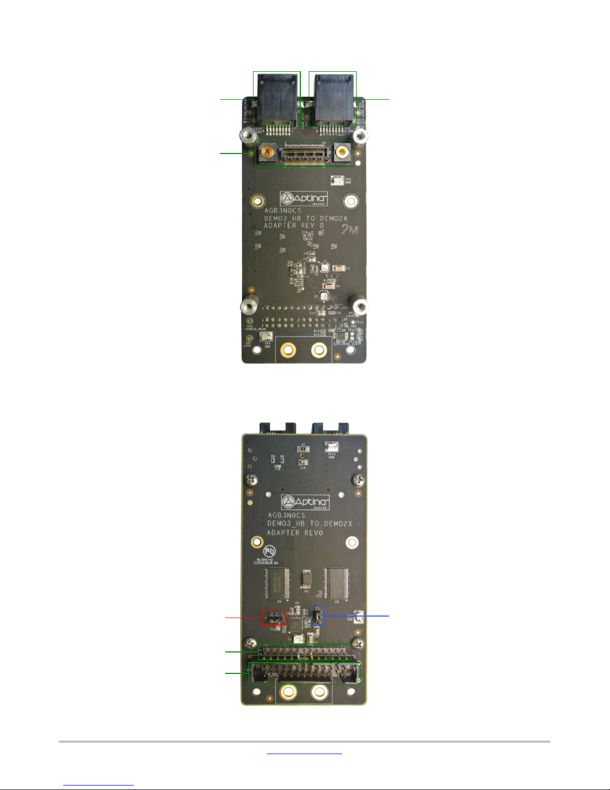
Top View
AGB3N0CS−GEVK
MIPI/HiSPi Connector J1 MIPI/HiSPi Connector J2
Demo 3 Headboard
Connector P6
Bottom View
Figure 3. Top View of Adapter Board with Connectors
Mode Selector P1
Demo 2× Baseboard
Connector P4
Demo 2× Baseboard
Connector P3
VDDIO Select P5
Figure 4. Bottom View of Adapter Board with Default Jumpers and Connectors
www.onsemi.com
2
Page 3

AGB3N0CS−GEVK
Jumper Pin Location
The jumpers on boards start with Pin 1 on the leftmost side
of the pin. Grouped jumpers increase in pin size with each
jumper added.
Figure 5. Pin Locations for a Single Jumper. Pin 1 is Located at the Leftmost Side
Pins 1−4Pin 1
Jumper/Header Functions & Default Positions
The P1 jumper/header configuration allows mode
selection to the Demo 2× Board. The 2−3 default jumper
position puts the Demo 2× in power safe mode, while the 1−2
jumper position puts the Demo 2× in Forced PWM mode.
The P5 jumper/header configuration allows for VDDIO
selection to the Demo 2× Board. The 2−3 default jumper
position connects VDDIO to +1.8 V, while the 1−2 jumper
position connects VDDIO to +2.8 V.
AGB3N0CS−GEVK Connectors
The adapter board supports has various different
connectors on-board, including a Demo 3 Headboard
connector, two MIPI/HiSPi connectors for the Demo 2×
Board, the 13-pin Demo 2× Board connector, and 26-pin
Demo 2× Board connector.
Baseboard Connectors
The Demo 2× Baseboard connectors are shown in the
pinout in Tables 1 and 2. The Demo 2× connectors has
a 14-pin and 26-pin connector, as well as two MIPI/HiSPi
connectors.
Table 1. 26-PIN DEMO 2X BASEBOARD CONNECTOR FUNCTION DESCRIPTION (P3)
Pin Name Description DIR Comment
1 S_DATA8 Parallel Data8 I/O Parallel Data Bit
2 S_DATA9 Parallel Data9 I/O Parallel Data Bit
3 S_DATA10 Parallel Data10 I/O Parallel Data Bit
4 S_DATA11 Parallel Data11 I/O Parallel Data Bit
5 S_DATA12 Parallel Data12 I/O Parallel Data Bit
6 S_DATA13 Parallel Data13 I/O Parallel Data Bit
7 S_DATA14 Parallel Data14 I/O Parallel Data Bit
8 S_DATA15 Parallel Data15 I/O Parallel Data Bit
9 S_DATA6 Parallel Data6 I/O Parallel Data Bit
10 S_DATA7 Parallel Data7 I/O Parallel Data Bit
11 GND Ground PWR
12 GND Ground PWR
13 S_LINE_VALID Parallel Line Valid Out Check Line Valid Signal
14 S_SP5 General Control Signal 5 Out Signal @ +3.3 V Level
15 NOT USED Not Used NA
16 HEAD_RESET_L Reset Signal to Sensor In Reset to Headboard Sensor
17 S_FRAME_VALID Parallel Frame Valid Out Check Frame Valid Signal
18 HEAD_SDA I2C Data to Sensor I/O Signal @ +3.3 V Level
19 HEAD_SCL I2C Clock to Sensor I/O Signal @ +3.3 V Level
20 NOT USED Not Used NA
21 +5V0_HEAD +5V0 Power Input PWR For Powering Up the Headboard
22 +5V0_HEAD +5V0 Power Input PWR For Powering Up the Headboard
23 S_PIXCLK Parallel Pixel Clock In Parallel Data Pixel Clock
24 GND Ground PWR
25 GND Ground PWR
26 MCLK Master Clock In Master Clock from Demo 3 Board
www.onsemi.com
3
Page 4

AGB3N0CS−GEVK
P
al
Table 2. 14-PIN DEMO 2X BASEBOARD CONNECTOR FUNCTION DESCRIPTION (P4)
Pin
1 GND Ground PWR
2 S_DATA4 Parallel Data4 I/O Parallel Data Bit
3 S_DATA5 Parallel Data5 I/O Parallel Data Bit
4 S_DATA2 Parallel Data2 I/O Parallel Data Bit
5 S_DATA3 Parallel Data3 I/O Parallel Data Bit
6 S_DATA0 Parallel Data0 I/O Parallel Data Bit
7 S_DATA1 Parallel Data1 I/O Parallel Data Bit
8 S_SP0 General Control Signal 0 Out Signal @ +3.3 V Level
9 S_SP1 General Control Signal 1 Out Signal @ +3.3 V Level
10 S_SP2 General Control Signal 2 Out Signal @ +3.3 V Level
11 S_SP3 General Control Signal 3 Out Signal @ +3.3 V Level
12 S_SP4 General Control Signal 4 Out Signal @ +3.3 V Level
13 +3V3_HEAD +3.3 V to Headboard PWR For Powering Up the Headboard
14 GND Ground PWR
Name Description DIR Comment
ON Semiconductor and the are registered trademarks of Semiconductor Components Industries, LLC (SCILLC) or its subsidiaries in the United States and/or other countries.
SCILLC owns the rights to a number of patents, trademarks, copyrights, trade secrets, and other intellectual property. A listing of SCILLC’s product/patent coverage may be accessed
at www.onsemi.com/site/pdf/ Patent− Marking.pdf . S CILLC reserves t he right to m ake changes wit hout further notice to any products h erein. SCILLC makes no warranty, representation
or guarantee regarding the suitability of its products for any particular purpose, nor does SCILLC assume any liability arising out of the application or use of any product or circuit, and
specifically disclaims any and all liability, including without limitation special, consequential or incidental damages. “Typical” parameters which may be provided in SCILLC data sheets
and/or specifications can and do vary in different applications and actual performance may vary over time. All operating parameters, including “Typicals” must be validated for each
customer application by customer’s technical e xperts. SCILLC does not convey any license under i ts p atent rights nor the rights of ot hers. S CILLC p roduct s a re n ot d esigned, i nt ended,
or authorized for use as components in systems intended for surgic al i mplant into the body, or other applications intended to s upport o r s ust ain life, or for any other application in which
the failure of the SCILLC product could create a situation where personal injury or death may occur. Should Buyer purchase or use SCILLC products for any such unintended or
unauthorized application, Buyer shall indemnify and hold SCILLC and its officers, em ployees, subsidiaries, affiliates, and distributors harmless against all claims, costs, damages, and
expenses, and reasonable at torney f ees a r ising o ut o f, d irectly o r indirectly, any claim o f p ersonal i njury o r d eath a ssociated w ith s uch u nintended o r u nauthorized u se, even if such claim
alleges that SCILLC was negligent r egarding the design o r manuf acture o f t he p art. SCILLC is an E qual O pportunity/Af firmative Action Employer. This literature is s ubject t o all applicable
copyright laws and is not for resale in any manner.
UBLICATION ORDERING INFORMATION
LITERATURE FULFILLMENT:
Literature Distribution Center for ON Semiconductor
19521 E. 32nd Pkwy, Aurora, Colorado 80011 USA
Phone: 303−675−2175 or 800−344−3860 Toll Free USA/Canada
Fax: 303−675−2176 or 800−344−3867 Toll Free USA/Canada
Email: orderlit@onsemi.com
N. American Technical Support: 800−282−9855 Toll Free
USA/Canada
Europe, Middle East and Africa Technical Support:
Phone: 421 33 790 2910
Japan Customer Focus Center
Phone: 81−3−5817−1050
www.onsemi.com
4
ON Semiconductor Website: www.onsemi.com
Order Literature: http://www.onsemi.com/orderlit
For additional information, please contact your loc
Sales Representative
EVBUM2313/D
 Loading...