

Page 1
ADM1024
System Hardware Monitor
with Remote Diode Thermal
Sensing
The ADM1024 is a complete system hardware monitor for
microprocessor-based systems, providing measurement and limit
comparison of various system parameters. Eight measurement inputs
are provided; three are dedicated to monitoring 5.0 V and 12 V power
supplies and the processor core voltage. The ADM1024 can monitor a
fourth power supply voltage by measuring its own V
(two pins) is dedicated to a remote temperature-sensing diode. Two
more pins can be configured as inputs to monitor a 2.5 V supply and a
second processor core voltage, or as a second temperature-sensing
input. The remaining two inputs can be programmed as general
purpose analog inputs or as digital fan speed measuring inputs.
Measured values can be read out via a serial System Management Bus
and values for limit comparisons can be programmed in over the same
serial bus. The high speed successive approximation ADC allows
frequent sampling of all analog channels to ensure a fast interrupt
response to any out-of-limit measurement.
The ADM1024’s 2.8 V to 5.5 V supply voltage range, low supply
current, and SMBus interface make it ideal for a wide range of
applications. These include hardware monitoring and protection
applications in personal computers, electronic test equipment, and office
electronics.
Features
• Up to Nine Measurement Channels
• Inputs Programmable-to-Measure Analog Voltage,
Fan Speed or External Temperature
• External Temperature Measurement with Remote Diode
(Two Channels)
• On-chip Temperature Sensor
• Five Digital Inputs for VID Bits
• LDCM Support
• System Management Bus (SMBus)
• Chassis Intrusion Detect
• Interrupt and Overtemperature Outputs
• Programmable RESET Input Pin
• Shutdown Mode to Minimize Power Consumption
• Limit Comparison of All Monitored Values
• This is a Pb-Free Device*
Applications
• Network Servers and Personal Computers
• Microprocessor-Based Office Equipment
• Test Equipment and Measuring Instruments
*For additional information on our Pb−Free strategy and soldering details, please
download the ON Semiconductor Soldering and Mounting Techniques
Reference Manual, SOLDERRM/D.
. One input
CC
www.onsemi.com
TSSOP−24
CASE 948H
PIN ASSIGNMENT
AD1024
241
232
223
214
205
196
187
178
169
1510
1411
1312
VID0/IRQ0
VID1/IRQ1
VID2/IRQ2
VID3/IRQ3
VID4/IRQ4
+V
CCP1
+2.5VIN/D2+
/D2−
V
CCP2
+5.0V
IN
+12V
IN
D1+
D1−
NTEST_OUT/ADD
THERM
SDA
SCL
FAN1/AIN1
FAN2/AIN2
GND
V
CC
INT
NTEST_IN/AOUT
RESET
CI
(Top View)
MARKING DIAGRAM
ADM
1024
ARUZ
1
Top Marking
#YYWW
ZZZZZZZZZ
CCCCCCCCCCC
Bottom Marking
YY = Year
WW = Work Week
ZZZZ = Assembly Lot Number
CCCC = Country of Origin
ORDERING INFORMATION
See detailed ordering and shipping information in the package
dimensions section on page 29 of this data sheet.
© Semiconductor Components Industries, LLC, 2016
January , 2016 − Rev. 5
1 Publication Order Number:
ADM1024/D
Page 2
VID0/IRQ0
VID1/IRQ1
VID2/IRQ2
VID3/IRQ3
VID4/IRQ4
V
CC
100k W
PULLUPS
VID0–3 AND
FAN DIVISOR
REGISTER
VID4 AND
DEVICE ID
REGISTER
ADM1024
ADM1024
SERIAL BUS
INTERFACE
CHANNEL
MODE
REGISTER
NTEST_OUT/ADD
SDA
SCL
FAN1/AIN1
FAN2/AIN2
+V
CCP1
+2.5VIN/D2+
+5.0V
+12V
V
/D2–
CCP2
D1+
D1–
V
IN
IN
CC
POWER TO CHIP
BAND GAP
TEMPERATURE
SENSOR
FAN SPEED
COUNTER
INPUT
ATTENUATORS
AND
ANALOG
MULTIPLEXER
ADDRESS
POINTER
REGISTER
TEMPERATURE
CONFIGURATION
REGISTER
10−BIT ADC
2.5V
BAND GAP
REFERENCE
GND
VALUE AND
LIMIT
REGISTERS
LIMIT
COMPARATORS
INTERRUPT
STATUS
REGISTERS
INT MASK
REGISTERS
INTERRUPT
MASKING
CONFIGURATION
REGISTERS
ANALOG
OUTPUT
REGISTER AND
8−BIT DAC
CHASSIS
INTRUSION
CLEAR
REGISTER
100k
100k W
100k W
V
CC
W
V
CC
V
CC
CI
THERM
INT
NTEST_IN/AOUT
RESET
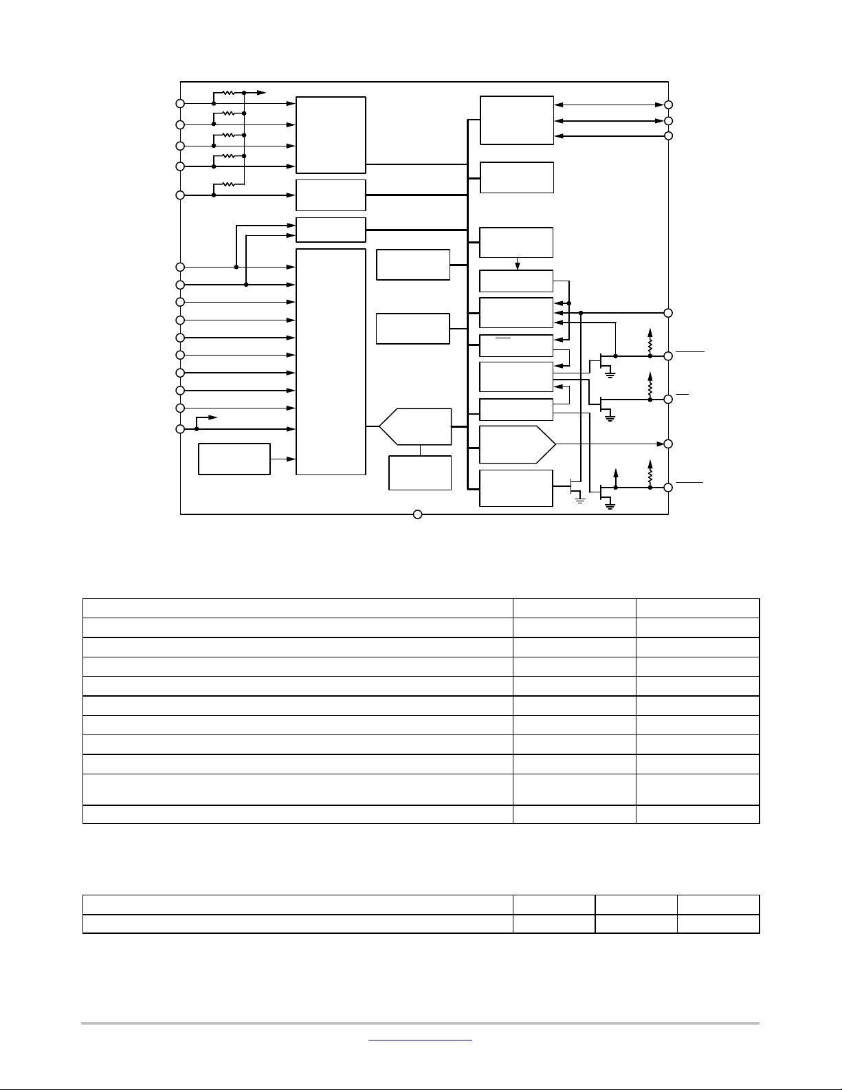
Figure 1. Functional Block Diagram
Table 1. ABSOLUTE MAXIMUM RATINGS
Parameter Rating Unit
Positive Supply Voltage (VCC) 6.5 V
Voltage on 12 VIN Pin 20 V
Voltage on AOUT, NTEST_OUT ADD, 2.5 VIN/D2+ −0.3 to (VCC + 0.3) V
Voltage on Any Other Input or Output Pin −0.3 to +6.5 V
Input Current at Any Pin ±5 mA
Package Input Current ±20 mA
Maximum Junction Temperature (T
Storage Temperature Range −65 to +150 °C
Lead Temperature, Soldering
Reflow Temperature
ESD Rating All Pins 2000 V
Stresses exceeding those listed in the Maximum Ratings table may damage the device. If any of these limits are exceeded, device functionality
should not be assumed, damage may occur and reliability may be affected.
NOTE: This device is ESD sensitive. Use standard ESD precautions when handling.
) 150 °C
JMAX
260
°C
Table 2. THERMAL CHARACTERISTICS
Package Type
q
JA
q
JC
24-Lead Small Outline Package 50 10 °C/W
Unit
www.onsemi.com
2
Page 3

ADM1024
Table 3. PIN ASSIGNMENT
Pin No. Mnemonic Description
1 NTEST_OUT/ADD Digital I/O. Dual function pin. This is a three-state input that controls the two LSBs of the Serial Bus
2 THERM Digital I/O. Dual function pin. This pin functions as an interrupt output for temperature interrupts only, or
3 SDA Digital I/O. Serial bus bidirectional data. Open-drain output.
4 SCL Digital Input. Serial bus clock.
5 FAN1/AIN1 Programmable Analog/Digital Input. 0 V to 2.5 V analog input or digital (0 to VCC) amplitude fan
6 FAN2/AIN2 Programmable Analog/Digital Input. 0 V to 2.5 V analog input or digital (0 to VCC) amplitude fan
7 CI Digital I/O. An active high input from an external latch that captures a Chassis Intrusion event. This line
8 GND System Ground.
9 V
CC
10 INT Digital Output. Interrupt request (open-drain). The output is enabled when Bit 1 of Register 40h is set to 1.
11 NTEST_IN/AOUT Digital Input/Analog Output. An active-high input that enables NAND Test mode board-level connectivity
12 RESET Digital I/O. Master Reset, 5 mA driver (open drain), active low output with a 45 ms minimum pulse width.
13 D1− Analog Input. Connected to cathode of first external temperature-sensing diode.
14 D1+ Analog Input. Connected to anode of first external temperature-sensing diode.
15 +12 V
16 +5.0 V
17 V
IN
IN
/D2– Programmable Analog Input. Monitors second processor core voltage or cathode of second external
CCP2
18 +2.5 VIN/D2+ Programmable Analog Input. Monitors 2.5 V supply or anode of second external temperature-sensing
19 +V
CCP1
20 VID4/IRQ4 Digital Input. Core Voltage ID readouts from the processor. This value is read into the VID4 Status
21 VID3/IRQ3 Digital Input. Core Voltage ID readouts from the processor. This value is read into the VID0–VID3 Status
22 VID2/IRQ2 Digital Input. Core Voltage ID readouts from the processor. This value is read into the VID0–VID3 Status
23 VID1/IRQ1 Digital Input. Core Voltage ID readouts from the processor. This value is read into the VID0–VID3 Status
24 VID0/IRQ0 Digital Input. Core Voltage ID readouts from the processor. This value is read into the VID0–VID3 Status
Address. This pin functions as an output when doing a NAND test.
as an interrupt input for fan control. It has an on-chip 100 kW pullup resistor.
tachometer input.
tachometer input.
can go high without any clamping action, regardless of the powered state of the ADM1024. The
ADM1024 provides an internal open drain on this line, controlled by Bit 6 of Register 40h or Bit 7 of
Register 46h, to provide a minimum 20 ms pulse on this line to reset the external Chassis Intrusion Latch.
Power (2.8 V to 5.5 V). Typically powered from 3.3 V power rail. Bypass with the parallel combination of
10 mF (electrolytic or tantalum) and 0.1 mF (ceramic) bypass capacitors.
The default state is disabled. It has an on-chip 100 kW pullup resistor.
testing. Refer to the section on NAND testing. Also functions as a programmable analog output when
NAND Test is not selected.
Set using Bit 4 in Register 40h. Also acts as reset input when pulled low (e.g., power-on reset). It has an
on-chip 100 kW pullup resistor.
Programmable Analog Input. Monitors 12 V supply.
Analog Input. Monitors 5.0 V supply.
temperature-sensing diode.
diode.
Analog Input. Monitors first processor core voltage (0 V to 3.6 V).
Register. Can also be reconfigured as an interrupt input. It has an on-chip 100 kW pullup resistor.
Register. Can also be reconfigured as an interrupt input. It has an on-chip 100 kW pullup resistor.
Register. Can also be reconfigured as an interrupt input. It has an on-chip 100 kW pullup resistor.
Register. Can also be reconfigured as an interrupt input. It has an on-chip 100 kW pullup resistor.
Register. Can also be reconfigured as an interrupt input. It has an on-chip 100 kW pullup resistor.
www.onsemi.com
3
Page 4

ADM1024
Table 4. ELECTRICAL CHARACTERISTICS (T
Parameter
= T
MIN
to T
A
MAX
, VCC = V
MIN
to V
, unless otherwise noted. (Note 1 and 2))
MAX
Test Conditions/Comments Min Typ Max Unit
POWER SUPPLY
Supply Voltage, V
Supply Current, I
CC
CC
Interface Inactive, ADC Active
ADC Inactive, DAC Active
Shutdown Mode
2.8 3.3 5.5 V
−
−
−
1.4
1.0
45
3.5
−
145
TEMPERATURE-TO-DIGITAL CONVERTER
Internal Sensor Accuracy
0°C ≤ TA ≤ 100°C
T
= 25°C
A
−
−
−
−
±3.0
±2.0
Resolution − ±1.0 − °C
External Diode Sensor Accuracy 0°C ≤ TA ≤ 100°C
25°C
−
−
−
±3.0
±5.0
−
Resolution − ±1.0 − °C
Remote Sensor Source Current High level
Low level
80
4.0
110
6.5
150
9.0
ANALOG-TO-DIGITAL CONVERTER (Including MUX and ATTENUATORS)
Total Unadjusted Error (TUE) (12 V
TUE (AIN, V
, 2.5 VIN, 5.0 VIN) − − ±3.0 %
CCP
) (Note 3) − − ±4.0 %
IN
Differential Non-linearity (DNL) − − ±1.0 LSB
Power Supply Sensitivity − ±1.0 − %/V
Conversion Time
(Note 4) − 754.8 856.8
(Analog Input or Internal Temperature)
Conversion Time (External Temperature) (Note 4) − 9.6 − ms
Input Resistance (2.5 V, 5.0 V, 12 V, V
Input Resistance (A
, A
) − 5.0 −
IN1
IN2
CCP1
, V
) 80 140 200
CCP2
ANALOG OUTPUT
Output Voltage Range
0 − 2.5 V
Total Unadjusted Error (TUE) IL = 2 mA − − ±3.0 %
Full-Scale Error − ±1.0 ±5.0 %
Zero-Scale Error No Load − 2.0 − LSB
Differential Non-linearity (DNL) Monotonic by Design − − ±1.0 LSB
Integral Non-linearity − ±1.0 − LSB
Output Source Current − 2.0 − mA
Output Sink Current − 1.0 − mA
FAN RPM-TO-DIGITAL CONVERTER
Accuracy
0°C ≤ TA ≤ 100°C − − ±12 %
Full-Scale Count − − 255
FAN1 to FAN2 Nominal Input RPM (Note 5) Divisor = 1, Fan Count = 153
Divisor = 2, Fan Count = 153
Divisor = 3, Fan Count = 153
Divisor = 4, Fan Count = 153
−
−
−
−
8800
4400
2200
1100
−
RPM
−
−
−
Internal Clock Frequency 0°C ≤ TA ≤ 100°C 19.8 22.5 25.2 kHz
DIGITAL OUTPUTS (NTEST_OUT)
Output High Voltage, V
Output Low Voltage, V
OH
OL
I
= +3.0 mA, VCC = 2.85 V −3.60 V 2.4 − − V
OUT
I
= −3.0 mA, VCC = 2.85 V −3.60 V − − 0.4 V
OUT
OPEN-DRAIN DIGITAL OUTPUTS (INT, THERM, RESET) (Note 6)
Output Low Voltage, V
OL
High Level Output Leakage Current, I
OH
I
= 3.0 mA, VCC = 3.60 V − − 0.4 V
OUT
V
OUT
= V
CC
− 0.1 100
RESET and CI Pulsewidth 20 45 − ms
mA
mA
°C
°C
mA
ms
kW
MW
mA
www.onsemi.com
4
Page 5

ADM1024
Table 4. ELECTRICAL CHARACTERISTICS (T
A
= T
MIN
to T
MAX
, VCC = V
MIN
to V
, unless otherwise noted. (Note 1 and 2))
MAX
Parameter UnitMaxTypMinTest Conditions/Comments
OPEN-DRAIN SERIAL DATABUS OUTPUT (SDA)
Output Low Voltage, V
OL
High Level Output Leakage Current, I
OH
I
= −3.0 mA, VCC = 2.85 V −3.60 V − − 0.4 V
OUT
V
OUT
= V
CC
− 0.1 100
mA
SERIAL BUS DIGITAL INPUTS (SCL, SDA)
Input High Voltage, V
Input Low Voltage, V
IH
IL
2.2 − − V
− − 0.8 V
Hysteresis − 500 − mV
Glitch Immunity − 100 − ns
DIGITAL INPUT LOGIC LEVELS (ADD, CI, RESET, VID0−VID4, FAN1, FAN2) (Note 7)
Input High Voltage, V
Input Low Voltage, V
IH
IL
VCC = 2.85 V − 5.5 V 2.2 − − V
VCC = 2.85 V − 5.5 V − − 0.8 V
NTEST_IN
Input High Current, I
IH
VCC = 2.85 V − 5.5 V 2.2 − −
V
DIGITAL INPUT CURRENT
Input High Current, I
Input Low Current, I
Input Capacitance, C
IH
IL
IN
VIN = V
CC
–1.0 − −
VIN = 0 − − 1.0
− 20 − pF
mA
mA
SERIAL BUS TIMING (Note 8)
Clock Frequency, f
Glitch Immunity, t
Bus Free Time, t
Start Setup Time, t
Start Hold Time, t
SCL Low Time, t
SCL High Time, t
SCLK
SW
BUF
SU; STA
HD; STA
LOW
HIGH
SCL, SDA Rise Time, t
SCL, SDA Fall Time, t
Data Setup Time, t
Data Hold Time, t
SU; DAT
HD; DAT
r
f
See Figure 2 − − 400 kHz
See Figure 2 − − 50 ns
See Figure 2 1.3 − −
See Figure 2 600 − −
See Figure 2 600 − −
See Figure 2 1.3 − −
See Figure 2 0.6 − −
ms
ns
ns
ms
ms
See Figure 2 − − 300 ns
See Figure 2 − − 300
ms
See Figure 2 100 − − ns
See Figure 2 − − 900 ns
1. All voltages are measured with respect to GND, unless otherwise specified.
2. Typicals are at T
3. TUE (Total Unadjusted Error) includes Offset, Gain, and Linearity errors of the ADC, multiplexer, and on-chip input attenuators, including
= 25°C and represent the most likely parametric norm. Shutdown current typ is measured with VCC = 3.3V.
A
an external series input protection resistor value between 0 kW and 1 kW.
4. Total monitoring cycle time is nominally m × 755 ms + n × 33244 ms, where m is the number of channels configured as analog inputs, plus 2
for the internal V
channels (D1 and D2).
measurement and internal temperature sensor, and n is the number of channels configured as external temperature
CC
5. The total fan count is based on two pulses per revolution of the fan tachometer output.
6. Open−drain digital o utputs m ay ha ve a n external p ullup r esistor connected t o a v oltage lower o r higher t han V
7. All logic inputs except ADD are tolerant of 5.0 V logic levels, even if V
, GND, or left open−circuit.
to V
CC
8. Timing specifications are tested at logic levels of VIL = 0.8 V for a falling edge and VIH = 2.2 V for a rising edge.
is less than 5.0 V. ADD is a three-state input that may be connected
CC
(up to 6.5 V absolute maximum).
CC
SCL
SDA
t
R
t
LOW
t
t
HD:STA
t
BUF
HD:DAT
t
HIGH
t
F
t
SU:DAT
t
SU:STA
t
HD:STA
t
SU:STO
PSPS
Figure 2. Serial Bus Timing Diagram
www.onsemi.com
5
Page 6
ADM1024
TYPICAL PERFORMANCE CHARACTERISTICS
30
20
10
0
–10
–20
–30
TEMPERATURE ERROR (°C)
–40
–50
–60
1 3.3 10 30
DXP TO VCC (5.0 V)
LEAK RESISTANCE (MΩ)
DXP TO GND
Figure 3. Temperature Error vs. PC Board
Track Resistance
25
20
15
10
5
TEMPERATURE ERROR (5C)
0
–5
50 500 5k 50k
FREQUENCY (Hz)
100mV p−p
25mV p−p
500k 5M
50mV p−p
100
50M
6
5
4
3
2
1
TEMPERATURE ERROR (5C)
0
–1
50 500 5k 50k
250mV p−p REMOTE
100mV p−p REMOTE
500k 5M
FREQUENCY (Hz)
Figure 4. Temperature Error vs. Power Supply
Noise Frequency
110
100
90
80
70
60
50
READING
40
30
20
10
0
0 10 20 30 40 50 60 70 80 90 100 110
MEASURED TEMPERATURE
50M
Figure 5. Temperature Error vs. Common-mode
Noise Frequency
25
20
15
10
5
TEMPERATURE ERROR (5C)
0
–5
1 2.2 3.2 4.7
DXP−DXN CAPACITANCE (nF)
7
Figure 7. Temperature Error vs. Capacitance
Between D+ and D–
Figure 6. Pentium) III Temperature vs. ADM1024
10
Figure 8. Temperature Error vs. Differential-mode
www.onsemi.com
6
10
9
8
7
6
5
4
3
TEMPERATURE ERROR (5C)
2
1
0
50 500 5k 50k
Reading
10mV SQ. WAVE
500k 5M 25M100k
FREQUENCY (Hz)
Noise Frequency
50M
Page 7

ADM1024
TYPICAL PERFORMANCE CHARACTERISTICS
26.5
26.0
25.5
25.0
24.5
24.0
STANDBY CURRENT (mA)
23.5
23.0
22.5
–40 –20 0 20 40 60 80 100 120
VDD = 3.3 V
TEMPERATURE (5C)
Figure 9. Standby Current vs. Temperature
www.onsemi.com
7
Page 8

ADM1024
General Description
The ADM1024 is a c omplete s ystem h ardware monitor for
microprocessor-based systems. The device communicates
with the system via a serial SMBus. The serial bus controller
has a hardwired address line for device selection (Pin 1), a
serial data line for reading and writing addresses and data
(SDA, Pin 14), and an input line for the serial clock (Pin 3),
and an input line for the serial clock (Pin 4). All control and
programming functions of the A DM1024 are performed o ver
the serial bus.
Measurement Inputs
Programmability of the measurement inputs makes the
ADM1024 extremely flexible and versatile. The device has
a 10−bit ADC and nine measurement input pins that can be
configured in different ways.
Pins 5 and 6 can be programmed as general-purpose
analog inputs with a range of 0 V to 2.5 V, or as digital inputs
to monitor the speed of fans with digital tachometer outputs.
The fan inputs can be programmed to accommodate fans
with different speeds and different numbers of pulses per
revolution from their tachometer outputs.
Pins 13 and 14 are dedicated temperature inputs and may
be connected to the cathode and anode of an external
temperature sensing diode.
Pins 15, 16, and 19 are dedicated analog inputs with
on-chip attenuators, configured to monitor 12 V, 5.0 V, and
the processor core voltage, respectively.
Pins 17 and 18 may be configured as analog inputs with
on-chip attenuators to monitor a s econd p rocessor core v oltage
and a 2.5 V supply, or they may be configured as a t emperature
input and connected to a second temperature-sensing diode.
The ADC also accepts input from an on-chip band gap
temperature sensor that monitors system-ambient temperature.
Finally, the ADM1024 monitors the supply from which it
is powered, so there is no need for a separate 3.3 V analog
input if the chip V
is 3.3 V. The range of this V
CC
CC
measurement can be configured for either a 3.3 V or 5.0 V
V
by Bit 3 of the Channel Mode Register.
CC
Sequential Measurement
When the ADM1024 monitoring sequence is started, it
cycles sequentially through the measurement of analog
inputs and the temperature sensor, while at the same time the
fan speed inputs are independently monitored. Measured
values from these inputs are stored in Value Registers. These
can be read out over the serial bus, or can be compared with
programmed limits stored in the Limit Registers. The results
of out-of-limit comparisons are stored in the Interrupt Status
Registers, and will generate an interrupt on the INT
line
(Pin 10).
Any or all of the Interrupt Status Bits can be masked by
appropriate programming of the Interrupt Mask Register.
Processor Voltage ID
Five digital inputs (VID4 to VID0−Pins 20 to 24) read the
processor voltage ID code. These inputs can also be
reconfigured as interrupt inputs.
The VID pins have internal 100 kW pullup resistors.
Chassis Intrusion
A chassis intrusion input (Pin 7) is provided to detect
unauthorized tampering with the equipment.
RESET
A RESET input/output (Pin 12) is provided. Pulling this
pin low will reset all ADM1024 internal registers to default
values. The ADM1024 can also be programmed to give a
low going 45 ms reset pulse at this pin.
Analog Output
The ADM1024 contains an on-chip, 8-bit DAC with an
output range of 0 V to 2.5 V (Pin 11). This is typically used
to implement a temperature-controlled fan by controlling
the speed of a fan dependent upon the temperature measured
by the on-chip temperature sensor.
Testing of board level connectivity is simplified by
providing a NAND tree test function. The AOUT (Pin 11)
also doubles as a NAND test input, while Pin 1 doubles as
a NAND tree output.
Internal Registers of the ADM1024
A brief description of the ADM1024’s principal internal
registers follows. More detailed information on the function
of each register is given in Table 10 to Table 23:
• Configuration Registers: Provide control and
configuration.
• Channel Mode Register: Stores the data for the
operating modes of the input channels.
• Address Pointer Register: This register contains the
address that selects one of the other internal registers.
When writing to the ADM1024, the first byte of data is
always a register address, which is written to the
Address Pointer Register.
• Interrupt (INT) Status Registers: Two registers to
provide status of each interrupt event. These registers
are also mirrored at addresses 4Ch and 4Dh.
• Interrupt (INT) Mask Registers: Allow masking of
individual interrupt sources.
• Temperature Configuration Register: The configuration
of the temperature interrupt is controlled by the lower
three bits of this register.
• VID/Fan Divisor Register: The status of the VID0 to
VID4 pins of the processor can be written to and read
from these registers. Divisor values for fan speed
measurement are also stored in this register.
www.onsemi.com
8
Page 9

ADM1024
• Value and Limit Registers: The results of analog
voltage inputs, temperature, and fan speed
measurements are stored in these registers, along with
their limit values.
• Analog Output Register: The code controlling the
analog output DAC is stored in this register.
• Chassis Intrusion Clear Register: A signal latched on
the chassis intrusion pin can be cleared by writing to
this register.
Serial Bus Interface
Control of the ADM1024 is carried out via the serial bus.
The ADM1024 is connected to this bus as a slave device,
under the control of a master device, e.g., ICH.
The ADM1024 has a 7-bit serial bus address. When the
device is powered up, it will do so with a default serial bus
address. The 5 MSBs of the address are set to 01011, and the
2 LSBs are determined by the logical states of Pin 1 (NTEST
OUT/ADD). This is a three-state input that can be grounded,
connected to V
addresses.
Table 5. ADD PIN TRUTH TABLE
ADD Pin A1 A0
GND 1 0
No Connect 0 0
V
CC
If ADD is left open-circuit, the default address will be
0101100. ADD is sampled only at powerup, so any changes
made while power is on will have no immediate effect.
The facility to make hardwired changes to A1 and A0
allows the user to avoid conflicts with other devices sharing
the same serial bus, for example, if more than one ADM1024
is used in a system.
The serial bus protocol operates as follows:
1. The master initiates data transfer by establishing a
START condition, defined as a high-to-low
transition on the serial data line SDA while the
serial clock line, SCL, remains high. This indicates
that an address/data stream will follow. All slave
peripherals connected to the serial bus respond to
the START condition, and shift in the next eight
bits, consisting of a 7-bit address (MSB first) plus
an R/W
data transfer, i.e., whether data will be written to
or read from the slave device.
The peripheral whose address corresponds to the
transmitted address responds by pulling the data
line low during the low period before the ninth
clock pulse, known as the Acknowledge Bit. All
other devices on the bus now remain idle while the
selected device waits for data to be read from or
written to it. If the R/W
write to the slave device. If the R/W
master will read from the slave device.
, or left open-circuit to give three different
CC
0 1
bit, which determines the direction of the
bit is a 0, the master will
bit is a 1, the
2. Data is sent over the serial bus in sequences of
nine clock pulses, eight bits of data followed by an
Acknowledge Bit from the slave device.
Transitions on the data line must occur during the
low period of the clock signal and remain stable
during the high period, as a low-to-high transition
when the clock is high may be interpreted as a
STOP signal. The number of data bytes that can be
transmitted over the serial bus in a single Read or
Write operation is limited only by what the master
and slave devices can handle.
3. When all data bytes have been read or written,
stop conditions are established. In Write mode, the
master will pull the data line high during the tenth
clock pulse to assert a STOP condition. In Read
mode, the master device will override the
Acknowledge Bit by pulling the data line high
during the low period before the ninth clock pulse.
This is known as No Acknowledge. The master
will then take the data line low during the low
period before the tenth clock pulse, then high
during the tenth clock pulse to assert a STOP
condition.
Any number of bytes of data may be transferred over the
serial bus in one operation, but it is not possible to mix read
and write in one operation because the type of operation is
determined at the beginning and cannot subsequently be
changed without starting a new operation.
In the case of the ADM1024, write operations contain
either one or two bytes, and read operations contain one byte
and perform the following functions.
To write data to one of the device data registers or read
data from it, the Address Pointer Register must be set so that
the correct data register is addressed, then data can be written
into that register or read from it. The first byte of a write
operation always contains an address that is stored in the
Address Pointer Register. If data is to be written to the
device, the write operation contains a second data byte that
is written to the register selected by the Address Pointer
Register. This is illustrated in Figure 10 The device address
is sent over the bus followed by R/W
set to 0. This is
followed by two data bytes. The first data byte is the address
of the internal data register to be written to, which is stored
in the Address Pointer Register. The second data byte is the
data to be written to the internal data register.
When reading data from a register, there are two
possibilities:
1. If the ADM1024’s Address Pointer Register value
is unknown or not the desired value, it is first
necessary to set it to the correct value before data
can be read from the desired data register. This is
done by performing a write to the ADM1024 as
before, but only the data byte containing the
register address is sent, as data is not to be written
to the register. This is shown in Figure 11.
A read operation is then performed consisting of
www.onsemi.com
9
Page 10
ADM1024
the serial bus address, R/W bit set to 1, followed
by the data byte read from the data register. This is
shown in Figure 12.
2. If the Address Pointer Register is known to be
already at the desired address, data can be read
1 991
SCL
0
SDA
START BY
MASTER
1011
FRAME 1
SERIAL BUS ADDRESS BYTE
SCL (CONTINUED)
SDA (CONTINUED)
Figure 10. Writing a Register Address to the Address Pointer Register,
then Writing Data to the Selected Register
A0
A1
R/W
ACK. BY
ADM1024
from the corresponding data register without first
writing to the Address Pointer Register, so
Figure 11 can be omitted.
D6
D7
1
D7
D5D6
D4 D3 D2 D1
D5
ADDRESS POINTER REGISTER BYTE
D4
FRAME 2
FRAME 3
DATA BYTE
D1D2D3
D0
D0
9
ACK. BY
ADM1024
ACK. BY
ADM1024
STOP BY
MASTER
19
SCL
SDA
START BY
MASTER
0
1 0 1 1 A1 A0
FRAME 1
SERIAL BUS ADDRESS BYTE
Figure 11. Writing to the Address Pointer Register Only
19
SCL
START BY
MASTER
0
0
1SDA
SERIAL BUS ADDRESS BYTE
1
FRAME 1
1
A1
Figure 12. Reading Data from a Previously Selected Register
NOTES
1. Although it is possible to read a data byte from a
data register without first writing to the Address
Pointer Register, if the Address Pointer Register is
already at the correct value, it is not possible to
write data to a register without writing to the
Address Pointer Register because the first data
byte of a write is always written to the Address
Pointer Register.
1
R/W
ACK. BY
ADM1024
A0
R/W
ACK. BY
ADM1024
D7
1
D6
D7
D4
D5D6
ADDRESS POINTER REGISTER BYTE
D5
FRAME 2
D4 D3 D2 D1
FRAME 2
DATA BYTE FROM ADM1024
D1D2D3
9
D0
ACK. BY
ADM1024
9
D0
NO ACK.
BY MASTER
STOP BY
MASTER
STOP BY
MASTER
2. In Figure 10 to Figure 12, the serial bus address is
shown as the default value 01011(A1)(A0), where
A1 and A0 are set by the three−state ADD pin.
Measurement Inputs
The ADM1024 has nine external measurement pins t hat can
be configured to perform various functions by programming
the Channel Mode Register.
www.onsemi.com
10
Page 11

ADM1024
Pins 13 and 14 are d edicated t o t emperature m easurement,
while Pins 1 5, 1 6, a nd 1 9 a re d edicated a nalog i nput c hannels.
Their function is unaffected by the Channel Mode Register.
Pins 5 and 6 can be individually programmed as analog
inputs, or as digital fan speed measurement inputs, by
programming Bits 0 and 1 of the Channel Mode Register.
Bit 3 of the Channel Mode Register configures the internal
V
measurement range for either 3.3 V or 5.0 V.
CC
Bits 4 to 6 of the Channel Mode Register enable or disable
Pins 22 to 24 when they are configured as interrupt inputs by
setting Bit 7 of the Channel Mode Register. This function is
controlled for Pins 20 and 21 by Bits 6 a nd 7 of Configuration
Register 2.
Pins 17 and 18 can be configured as analog inputs o r as i nputs
for external temperature-sensing diodes by programming Bit 2
of the Channel Mode Register.
Table 6. CHANNEL MODE REGISTER (Note 1)
Channel
Mode
Register Bit
0 5 0 = FAN1, 1 = A
1 6 0 = FAN2, 1 = A
2 17, 18 0 = 2.5 V, V
3 Int. V
4 24 0 = VID0, 1 = IRQ0
5 23 0 = VID1, 1 = IRQ1
6 22 0 = VID2, 1 = IRQ2
7 20–24 0 = VID0 to VID4,
1. Power-on Default = 0000 0000
Controls
Pin(s)
CC
Meas.
Function
IN1
IN2
, 1 = D2–, D2+
CCP2
0 = 3.3 V, 1 = 5.0 V
1 = Interrupt Inputs
A truth table for the Channel Mode Register is given in
Table 6.
Table 7. A/D OUTPUT CODE VS. V
+12 V
IN
<0.062 <0.026 <0.0172 <0.026 <0.013 <0.014 <0.010 0 00000000
0.062–0.125 0.026–0.052 0.017–0.034 0.026–0.052 0.013–0.026 0.014–0.028 0.010–0.019 1 00000001
0.125–0.188 0.052–0.078 0.034–0.052 0.052–0.078 0.026–0.039 0.028–0.042 0.019–0.029 2 00000010
0.188–0.250 0.078–0.104 0.052–0.069 0.078–0.104 0.039–0.052 0.042–0.056 0.029–0.039 3 00000011
0.250–0.313 0.104–0.130 0.069–0.086 0.104–0.130 0.052–0.065 0.056–0.070 0.039–0.049 4 00000100
0.313–0.375 0.130–0.156 0.086–0.103 0.130–0.156 0.065–0.078 0.070–0.084 0.049–0.058 5 00000101
0.375–0.438 0.156–0.182 0.103–0.120 0.156–0.182 0.078–0.091 0.084–0.098 0.058–0.068 6 00000110
0.438–0.500 0.182–0.208 0.120–0.138 0.182–0.208 0.091–0.104 0.098–0.112 0.068–0.078 7 00000111
0.500–0.563 0.208–0.234 0.138–0.155 0.208–0.234 0.104–0.117 0.112–0.126 0.078–0.087 8 00001000
4.000–4.063 1.666–1.692 1.100–1.117 1.666–1.692
8.000–8.063 3.330–3.560 2.200–2.217 3.330–3.560
12.000–12.063 5.000–5.026 3.300–3.317 5.000–5.026
15.312–15.375 6.380–6.406 4.210–4.230 6.380–6.406
15.375–15.437 6.406–6.432 4.230–4.245 6.406–6.432 3.203–3.216 3.459–3.473 2.402–2.412 246 11110110
15.437–15.500 6.432–6.458 4.245–4.263 6.432–6.458 3.216–3.229 3.473–3.487 2.412–2.422 247 11110111
15.500–15.563 6.458–6.484 4.263–4.280 6.458–6.484 3.229–3.242 3.487–3.501 2.422–2.431 248 11111000
15.563–15.625 6.484–6.510 4.280–4.300 6.484–6.510 3.242–3.255 3.501–3.515 2.431–2.441 249 11111001
15.625–15.688 6.510–6.536 4.300–4.314 6.510–6.536 3.255–3.268 3.515–3.529 2.441–2.451 250 11111010
15.688–15.750 6.536–6.562 4.314–4.331 6.536–6.562 3.268–3.281 3.529–3.543 2.451–2.460 251 11111011
15.750–15.812 6.562–6.588 4.331–4.348 6.562–6.588 3.281–3.294 3.543–3.558 2.460–2.470 252 11111100
15.812–15.875 6.588–6.615 4.348–4.366 6.588–6.615 3.294–3.307 3.558–3.572 2.470–2.480 253 11111101
+5.0 V
IN
IN
Input Voltage A/D Output
VCC (3.3 V) VCC (5.0 V) +2.5 V
−
−
−
0.833–0.846
−
−
−
1.667–1.680
−
−
−
2.500–2.513
−
−
−
3.190–3.203
+V
IN
CCP 1/2
0.900–0.914 0.625–0.635
1.800–1.814 1.250–1.260
2.700–2.714 1.875–1.885
3.445–3.459 2.392–2.402 245 11110101
A
IN (1/2)
Decimal Binary
64
(1/4−Scale)
128
(1/2−Scale)
192
(3/4−Scale)
01000000
10000000
11000000
www.onsemi.com
11
Page 12
ADM1024
A-to-D Converter
These inputs are multiplexed into the on-chip, successive
approximation, Analog-to-Digital Converter (ADC). This
has a resolution of eight bits. The basic input range is 0 V to
2.5 V, which is the input range of AIN1 and AIN2, but five
of the inputs have built-in attenuators to allow measurement
of 2.5 V, 5.0 V, 12 V, and the processor core voltages V
and V
without any external components. To allow for
CCP2
CCP1
the tolerance of these supply voltages, the ADC produces an
output of 3/4 full scale (decimal 192) for the nominal input
voltage, and so has adequate headroom to cope with
overvoltages. Table 7 shows the input ranges of the analog
inputs and output codes of the ADC.
When the A DC i s r unning, i t s amples a nd c onverts a n input
every 748 ms, except for the external temperature (D1 and
D2) inputs. These have special input signal c onditioning and
are averaged over 16 conversions to reduce noise, and a
measurement on one of these inputs takes nominally 9.6 ms.
Input Circuits
The internal structure for the analog inputs is shown in
Figure 13. Each input circuit consists of an input protection
diode, an attenuator, plus a capacitor to form a first-order
low-pass filter that gives the input immunity to high
frequency noise.
AIN1–AIN2
+12V
+5.0V
+2.5V
(SEE TEXT)
+V
CCP1/VCCP2
Figure 13. Structure of Analog Inputs
80kW
10pF
122.2k
IN
IN
IN
22.7k
91.6k
55.2k
36.7k
111.2k
42.7k
97.3k
W
W
W
W
W
W
W
W
35pF
25pF
25pF
50pF
MUX
R1
V
IN
Figure 14. Scaling A
AIN(1–2)
R2
IN(1−2)
Negative and bipolar input ranges can be accommodated
by using a positive reference voltage to offset the input
voltage range so it is always positive.
R1
R2
+
ǒ
V
f
* 2.5
s
2.5
Ǔ
(eq. 1)
To measure a negative input voltage, an attenuator can be
used as shown in Figure 15.
+V
OS
R2
R1
V
IN
Figure 15. Scaling and Offsetting A
AIN(1–2)
IN(1−2)
for Negative Inputs
This is a simple and cheap solution, but the following
point should be noted. Since the input signal is offset but not
inverted, the input range is transposed. An increase in the
magnitude of the −12 V supply (going more negative) will
cause the input voltage to fall and give a lower output code
from the ADC. Conversely, a decrease in the magnitude of
the −12 V supply will cause the ADC code to increase. The
maximum negative voltage corresponds to zero output from
the ADC. This means that the upper and lower limits will be
transposed.
V
*
f
+
s
Ť
Ť
V
OS
(eq. 2)
R1
R2
Bipolar input ranges can easily be accommodated. By
making R1 equal to R2 and V
= 2.5 V, the input range is
OS
±2.5 V. Other input ranges can be accommodated by adding
a third resistor to set the positive full−scale input voltage.
+V
OS
2.5 V Input Precautions
When using the 2.5 V input, the following precautions
should be noted. There is a parasitic diode between Pin 18
and V
due to the presence of a PMOS current source
CC
(which is used when Pin 18 is configured as a temperature
input). This will become forward biased if Pin 18 is more
than 0.3 V above V
. Therefore, VCC should never be
CC
powered off with a 2.5 V input connected.
Setting Other Input Ranges
A
IN1
and A
can easily be scaled to voltages other than
IN2
2.5 V. If the input voltage range is zero to some positive
voltage, all that is required is an input attenuator, as shown
in Figure 14.
www.onsemi.com
R2
V
R1
IN
Figure 16. Scaling and Offsetting A
AIN(1–2)
R3
IN(1−2)
for Bipolar Inputs
(R3 has no effect as the input voltage at the device pin is zero
when V
12
= minus full scale.)
IN
R1
R2
+
Ť
Ť
V
*
f
s
R2
(eq. 3)
Page 13
ADM1024
(R2 has no effect as the input voltage at the device pin is
2.5 V when V
= plus full scale).
IN
ǒ
R1
R3
V
+
f
s)
* 2.5
2.5
Ǔ
(eq. 4)
Offset voltages other than 2.5 V can be used, but the
calculation becomes more complicated.
Temperature Measurement System
Local Temperature Measurement
The ADM1024 contains an on-chip band gap temperature
sensor, whose output is digitized by the on-chip ADC. The
temperature data is stored in the Temperature Value Register
(address 27h) and the LSB from Bits 6 and 7 of the
Temperature Configuration Register (address 4Bh). As both
positive and negative temperatures can be measured, the
temperature data is stored in twos complement format, as
shown in Table 8. Theoretically, the temperature sensor and
ADC can measure temperatures from −128°C to +127°C
with a resolution of 1°C, although temperatures below
−40°C and above +125°C are outside the operating
temperature range of the device.
External Temperature Measurement
The ADM1024 can measure the temperature of two
external diode sensors or diode-connected transistors,
connected to Pins 13 and 14 or 17 and 18.
Pins 13 and 14 are a dedicated temperature input channel.
Pins 17 and 18 can be configured to measure a diode sensor
by setting Bit 2 of the Channel Mode Register to 1.
The forward voltage of a diode or diode-connected
transistor, operated at a constant current, exhibits a negative
temperature coefficient of about –2 mV/°C. Unfortunately,
the absolute value of V
varies from device to device, and
BE
individual calibration is required to null this out, so the
technique is unsuitable for mass production.
The technique used in the ADM1024 is to measure the
change in V
when the device is operated at two different
BE
currents.
This is given by:
DVbe+ KTńq ln(N
)
(eq. 5)
where:
K is Boltzmann’s constant.
q is the charge on the carrier.
T is the absolute temperature in Kelvins.
N is the ratio of the two currents.
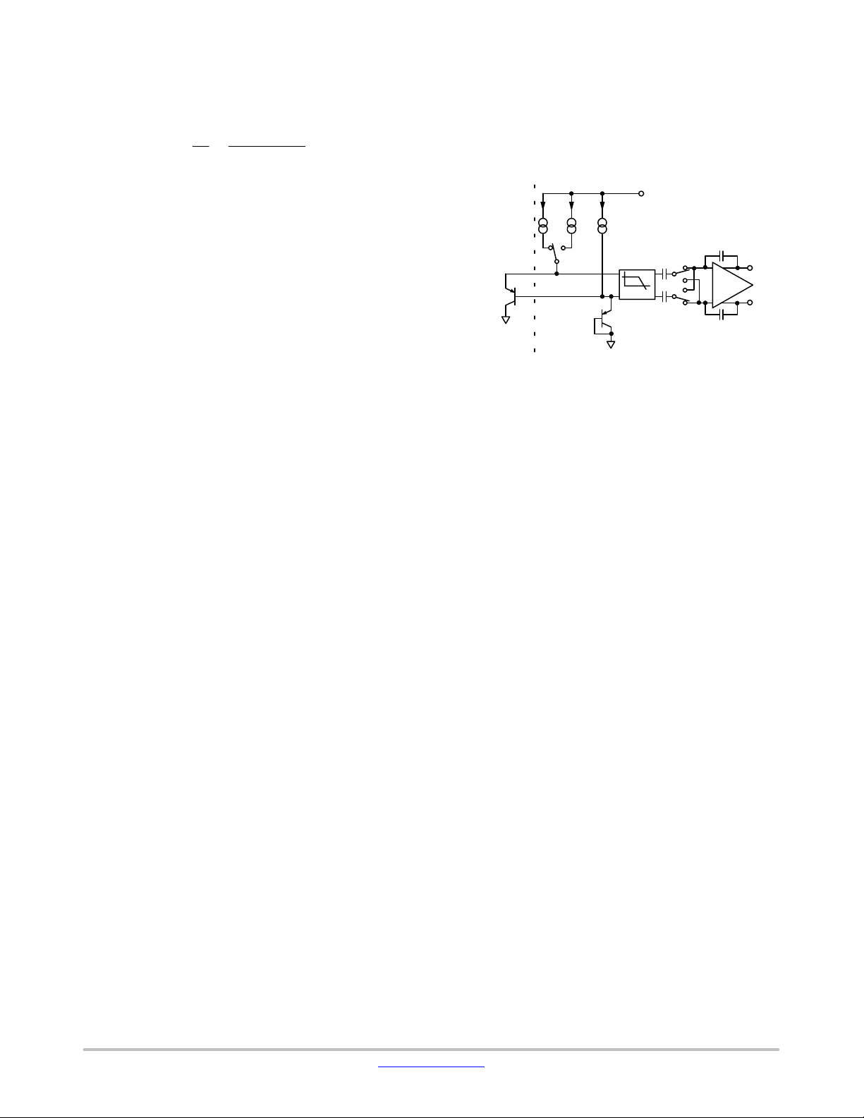
Figure 17 shows the input signal conditioning used to
measure the output of an external temperature sensor. This
figure shows the external sensor as a substrate transistor
provided for temperature monitoring on some
microprocessors, but it could equally well be a discrete
transistor.
V
DD
N y I
REMOTE
SENSING
TRANSISTOR
I
D+
D–
BIAS
DIODE
I
BIAS
LOW−PASS
FILTER
f
C
= 65kHz
LPF
V
V
OUT+
ADC
OUT–
TO
Figure 17. Signal Conditioning for External Diode
Temperature Sensors
If a discrete transistor is used, the collector will not be
grounded and should be linked to the base. If a PNP
transistor is used, the base is connected to the D− input and
the emitter to the D+ input. If an NPN transistor is used, the
emitter is connected to the D− input and the base to the D+
input.
To prevent ground noise from interfering with the
measurement, the more negative terminal of the sensor is not
referenced to ground, but is biased above ground by an
internal diode at the D− input. As the sensor is operating in
a noisy environment, C1 is provided as a noise filter. See the
Layout Considerations section for more information on C1.
To measure DV
, the sensor is switched between
BE
operating currents of I and N × I. The resulting waveform is
passed through a 65 kHz low−pass filter to remove noise,
then to a chopper−stabilized amplifier that performs the
functions of amplification and rectification of the waveform
to produce a dc voltage proportional to DV
. This voltage
BE
is measured by the ADC to give a temperature output in 8-bit
twos complement format. To further reduce the effects of
noise, digital filtering is performed by averaging the results
of 16 measurement cycles. An external temperature
measurement takes nominally 9.6 ms.
The results of external temperature measurements are
stored in 8-bit, twos complement format, as illustrated in
Table 8.
www.onsemi.com
13
Page 14

ADM1024
Table 8. TEMPERATURE DATA FORMAT
Temperature Digital Output
−128°C 1000 0000
−125°C 1000 0011
−100°C 1001 1100
−75°C 1011 0101
−50°C 1100 1110
−25°C 1110 0111
0°C 0000 0000
+0.5°C 0000 0000
+10°C 0000 1010
+25°C 0001 1001
+50°C 0011 0010
+75°C 0100 1011
+100°C 0110 0100
+125°C 0111 1101
+127°C 0111 1111
Layout Considerations
Digital boards can be electrically noisy environments, and
care must be taken to protect the analog inputs from noise,
particularly when measuring the very small voltages from a
remote diode sensor. The following precautions should be
taken:
1. Place the ADM1024 as close as possible to the
remote sensing diode. Provided that the worst
noise sources such as clock generators,
data/address buses, and CRTs are avoided, this
distance can be 4 inches to 8 inches.
2. Route the D+ and D− tracks close together, in
parallel, with grounded guard tracks on each side.
Provide a ground plane under the tracks if
possible.
3. Use wide tracks to minimize inductance and
reduce noise pickup. A 10 mil track minimum
width and spacing is recommended.
10MIL
GND
D+
D–
GND
Figure 18. Arrangement of Signal Tracks
10MIL
10MIL
10MIL
10MIL
10MIL
10MIL
10MIL
10MIL
10MIL
10MIL
4. Try to minimize the number of copper/solder joints,
which can cause thermocouple effects. Where
copper/solder joints are used, make sure that they
are in both the D+ and D– path and at the same
temperature. Thermocouple effects should not be a
major problem as 1°C corresponds to about 240 mV,
and thermocouple voltages are about 3 mV/°C of
temperature difference. Unless there are two
thermocouples with a big temperature differential
between them, thermocouple voltages should be
much less than 200 mV.
5. Place 0.1 mF bypass and 2200 pF input filter
capacitors close to the ADM1024.
6. If the distance to the remote sensor is more than
8 inches, the use of twisted pair cable is
recommended. This will work up to about 6 feet to
12 feet.
7. For really long distances (up to 100 feet) use
shielded twisted pair such as Belden #8451
microphone cable. Connect the twisted pair to D+
and D– and the shield to GND close to the
ADM1024. Leave the remote end of the shield
unconnected to avoid ground loops.
Because the measurement technique uses switched
current sources, excessive cable and/or filter capacitance
can affect the measurement. When using long cables, the
filter capacitor may be reduced or removed.
Cable resistance can also introduce errors. A 1 W series
resistance introduces about 0.5°C error.
Limit Values
Limit values for analog measurements are stored in the
appropriate limit registers. In the case of voltage
measurements, high and low limits can be stored so that an
interrupt request will be generated if the measured value
goes above or below acceptable values. In the case of
temperature, a Hot Temperature or High Limit can be
programmed, and a Hot Temperature Hysteresis or Low
Limit, which will usually be some degrees lower. This can
be useful as it allows the system to be shut down when the
hot limit is exceeded, and restarted automatically when it has
cooled down to a safe temperature.
Monitoring Cycle Time
The monitoring cycle begins when a 1 is written to the
Start Bit (Bit 0), and a 0 to the INT
Configuration Register. INT
1 to enable the INT
output. The ADC measures each analog
_Clear Bit (Bit 3) of the
_Enable (Bit 1) should be set to
input in turn; as each measurement is completed, the result
is automatically stored in the appropriate value register. This
“round robin” monitoring cycle continues until it is disabled
by writing a 0 to Bit 0 of the Configuration Register.
As the ADC will normally be left to free-run in this
manner, the time taken to monitor all the analog inputs will
normally not be of interest, as the most recently measured
value of any input can be read out at any time.
For applications where the monitoring cycle time is
important, it can be calculated as follows:
m t1) n t
2
(eq. 6)
where:
m − the number of inputs configured as analog inputs, plus the
internal V
measurement and internal temperature sensor.
CC
www.onsemi.com
14
Page 15

ADM1024
t
the time taken for an analog input conversion, nominally
1 −
6.044 ms.
n − the number of inputs configured as external temperature
inputs.
t
the time taken for a temperature conversion, nominally
2 −
33.24 ms.
This rapid sampling of the analog inputs ensures a quick
response in the event of any input going out of limits, unlike
other monitoring chips that employ slower ADCs.
Fan Monitoring Cycle Time
When a monitoring cycle is started, monitoring of the fan
speed inputs begins at the same time as monitoring of the
analog inputs. However, the two monitoring cycles are not
synchronized in any way. The monitoring cycle time for the
fan inputs is dependent on fan speed and is much slower than
for the analog inputs. For more details, see the Fan Speed
Measurement section.
Input Safety
Scaling of the analog inputs is performed on-chip, so
external attenuators are normally not required. However,
since the power supply voltages will appear directly at the
pins, it is advisable to add small external resistors in series
with the supply traces to the chip to prevent damaging the
traces or power supplies should an accidental short such as
a probe connect two power supplies together.
As the resistors will form part of the input attenuators,
they will affect the accuracy of the analog measurement if
their value is too high. The analog input channels are
calibrated assuming an external series resistor of 500 W, and
the accuracy will remain within specification for any value
from 0 kW to 1 kW, so a standard 510 W resistor is suitable.
The worst such accident would be connecting −2.0 V to
+12 V , a t otal o f 24 V d ifference. W ith the series r esistors, this
would draw a maximum current of approximately 24 mA.
Analog Output
The ADM1024 has a single analog output from an
unsigned 8-bit DAC that produces 0 V to 2.5 V. The analog
output register defaults to FF during power-on reset, which
produces maximum fan speed. The analog output may be
amplified and buffered with external circuitry such a s an op
amp and transistor to provide fan speed control.
Suitable fan drive circuits are given in Figure 19 to Figure 24.
When using any of these circuits, the following points should be
noted:
1. All of these circuits will provide an output range
from 0 V to almost 12 V, apart from Figure 25
which loses the base−emitter voltage drop of Q1
due to the emitter−follower configuration.
2. To amplify the 2.5 V range of the analog output up
to 12 V, the gain of these circuits needs to be
around 4.8.
3. Care must be taken when choosing the op amp to
ensure that its input common-mode range and
output voltage swing are suitable.
4. The op amp may be powered from the 12 V rail
alone or from 12 V. If it is powered from 12 V,
then the input common-mode range should include
ground to accommodate the minimum output
voltage of the DAC, and the output voltage should
swing below 0.6 V to ensure that the transistor can
be turned fully off.
5. If the op amp is powered from −12 V, precautions
such as a clamp diode to ground may be needed to
prevent the base-emitter junction of the output
transistor being reverse-biased in the unlikely
event that the output of the op amp should swing
negative for any reason.
12V
1/4
AOUT
Figure 19. Fan Drive Circuit with Op Amp and
AOUT
Figure 20. Fan Drive Circuit with Op Amp and PNP
AOUT
Figure 21. Fan Driver Circuit with Op Amp and
LM324
R2
36kΩ
R1
10kΩ
Emitter-Follower
R4
R3
1kΩ
R2
39kΩ
1kΩ
R1
10kΩ
1/4
LM324
Transistor
R3
100kΩ
R2
39kΩ
R1
10kΩ
1/4
LM324
P-Channel MOSFET
12V
Q1
2N2219A
Q1
BD136
2SA968
12V
Q1
IRF9620
www.onsemi.com
15
Page 16

ADM1024
12V
AOUT
R1
100kΩ
MBT3904
Q1/Q2
DUAL
R2
100kΩ
R3
3.9kΩ
R4
1kΩ
Q3
IRF9620
Figure 22. Discrete Fan Drive Circuit with P-Channel
MOSFET, Single Supply
12V
R2
AOUT
MTB3904
R1
4.7kΩ
Q1/Q2
DUAL
–12V
100kΩ
R3
39kΩ
R4
10kΩ
Q3
IRF9620
Figure 23. Discrete Fan Drive Circuit with P-Channel
MOSFET, Dual Supply
12V
AOUT
R1
100kΩ
MBT3904
Q1/Q2
DUAL
R2
100kΩ
R5
100kΩ
Q3
BC556
2N3906
R3
3.9kΩ
R4
1kΩ
Q4
BD132
TIP32A
Figure 24. Discrete Fan Drive Circuit with Bipolar
Output, Dual Supply
6. In all these circuits, the output transistor must have
an I
greater than the maximum fan current,
CMAX
and be capable of dissipating power due to the
voltage dropped across it when the fan is not
operating at full speed.
7. If the fan motor produces a large back EMF when
switched off, it may be necessary to add clamp
diodes to protect the output transistors in the event
that the output goes very quickly from full scale to
zero.
Fault-Tolerant Fan Control
The ADM1024 incorporates a fault-tolerant fan control
capability that can override the setting of the analog output
and force it to maximum to give full fan speed in the event
of a critical overtemperature problem even if, for some
reason, this has not been handled by the system software.
There are four temperature set points that will force the
analog output to FFh if any one of them is exceeded for three
or more consecutive measurements. Two of these limits are
programmable by the user and two are hardware limits
intended as must not exceed limits that cannot be changed.
The analog output will be forced to FFh if:
The temperature measured by the on-chip sensor exceeds
the limit programmed into register address 13hp;
or:
The temperature measured by either of the remote sensors
exceeds the limit programmed into address 14h;
or:
The temperature measured by the on-chip sensor exceeds
70°C, which is hardware programmed into a read-only
register at address 17h;
or:
The temperature measured by either of the remote sensors
exceeds 85°C, which is hardware programmed into a
read-only register at address 18h.
Once the hardware override of the analog output is
triggered, it will return to normal operation only after three
consecutive measurements that are 5 degrees lower than
each of the above limits.
The analog output can also be forced to FFh by pulling the
THERM
pin (Pin 2) low.
The limits in Registers 13h and 14h can be programmed
by the user. Obviously, these limits should not exceed the
hardware values in Registers 17h and 18h, as they would
have no effect. The power-on default values of these
registers are the same as the two hardware registers, 70°C
and 85°C, respectively, so there is no need to program them
if these limits are acceptable.
Once these registers have been programmed, or if the
defaults are acceptable, the values in these registers can be
locked by writing a 1 to Bits 1 and 2 of Configuration
Register 2 (address 4Ah). This prevents any unauthorized
tampering with the limits. These lock bits can only be
written to 1 and can only be cleared by power-on reset or by
taking the RESET
pin low, so registers 13h and 14h cannot
be written to again unless the device is powered off, then on.
Layout and Grounding
Analog inputs will provide best accuracy when referred to
a clean ground. A separate, low impedance ground plane for
analog ground, which provides a ground point for the
www.onsemi.com
16
Page 17

ADM1024
)
2
R2
5.0 V
voltage dividers and analog components, will provide best
performance but is not mandatory.
The power supply bypass, the parallel combination of
10 mF (electrolytic or tantalum) and 0.1 mF (ceramic) bypass
capacitors connected between Pin 9 and ground, should also
be located as close as possible to the ADM1024.
Fan Inputs
Pins 5 and 6 may be configured as analog inputs or fan
speed inputs by programming Bits 0 and 1 of the Channel
Mode Register. The power-on default for these bits is all
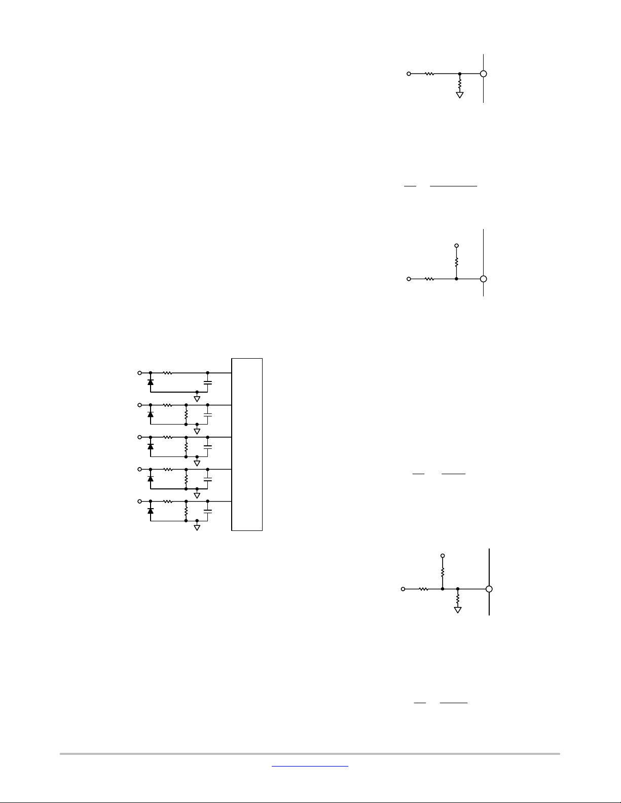
zeros, which makes Pins 5 and 6 fan inputs.
Signal conditioning in the ADM1024 accommodates the
slow rise and fall times typical of fan tachometer outputs.
The maximum input signal range is 0 to V
. In the event
CC
that these inputs are supplied from fan outputs that exceed
0 V to 6.5 V, either resistive attenuation of the fan signal or
diode clamping must be included to keep inputs within an
acceptable range.
Figure 25 to Figure 28 show circuits for most common fan
tachometer outputs.
If the fan tachometer output has a resistive pullup to V
CC
it can be directly connected to the fan input, as shown in
Figure 25.
V
160k
W
CC
FAN SPEED
COUNTER
CC
12V
PULLUP
4.7k
W
TYP
FAN1 OR
TACH
OUTPUT
FAN2
Figure 25. Fan with Tach Pullup to +V
If the fan output has a resistive pullup to 12 V (or other
voltage greater than 6.5 V), the fan output can be clamped
with a Zener diode, as shown in Figure 26. The Zener
voltage should be chosen so it is greater than V
but less
IH
than 6.5 V, allowing for the voltage tolerance of the Zener.
A value of between 3.0 V and 5.0 V is suitable.
12V
PULLUP
4.7k
W
TYP
*
CHOOSE ZD1 VOLTAGE APPROXIMATELY 0.8 y VCC.
TACH
OUTPUT
FAN1 OR
FAN2
ZD1
ZENER
*
Figure 26. Fan with Tach. Pullup to Voltage >6.5 V
(e.g., 12 V) Clamped with Zener Diode
160k
V
CC
W
FAN SPEED
COUNTER
If the fan has a strong pullup (less than 1 kW) to 12 V, or
a totem-pole output, then a series resistor can be added to
limit the Zener current, as shown in Figure 27. Alternatively,
a resistive attenuator may be used, as shown in Figure 28.
R1 and R2 should be chosen such that:
.0 V t V
t
PULLUP
ǒ
R
PULLUP
) R1 ) R2
t
Ǔ
The fan inputs have an input resistance of nominally
160 kW to ground, so this should be taken into account when
calculating resistor values.
With a pullup voltage of 12 V and pullup resistor less than
1 kW, suitable values for R1 and R2 would be 100 kW and
47 kW. This will give a high input voltage of 3.83 V.
12V
PULLUP
TYP <1k ORW
TOTEM−POLE
,
*
CHOOSE ZD1 VOLTAGE APPROXIMATELY 0.8 y V
R1
10kW
TACH
OUTPUT
FAN1 OR
FAN2
*
ZD1
ZENER
160kW
Figure 27. Fan with Strong Tach Pullup to >VCC or
Totem Pole Output, Clamped with Zener and Resistor
12V
<1k W
*
SEE TEXT.
*
R1
TACH
OUTPUT
FAN1 OR
FAN2
R2
*
160k
V
CC
W
Figure 28. Fan with Strong Tach Pullup to > VCC or
Totem Pole Output, Attenuated with R1/R2
Fan Speed Measurement
The fan counter does not count the fan tachometer output
pulses directly because the fan speed may be less than
1000 rpm and it would take several seconds to accumulate
a reasonably large and accurate count. Instead, the period of
the fan revolution is measured by gating an on-chip
22.5 kHz oscillator into the input of an 8-bit counter for two
periods of the fan tachometer output, as shown in Figure 29;
the accumulated count is actually proportional to the fan
tachometer period and inversely proportional to the fan
speed.
(eq. 7
V
CC
FAN SPEED
COUNTER
FAN SPEED
COUNTER
CC
www.onsemi.com
17
Page 18

ADM1024
22.5kHz
CLOCK
CONFIG.
REG. 1 BIT 0
FAN1
INPUT
FAN2
INPUT
START OF
MONITORING
CYCLE
Figure 29. Fan Speed Measurement
FAN1
MEASUREMENT
PERIOD
FAN2
MEASUREMENT
PERIOD
The monitoring cycle begins when a one is written to the
Start Bit (Bit 0), and a zero to the INT
the Configuration Register. INT
set to one to enable the INT
output. The measurement begins
_Clear Bit (Bit 3) of
_Enable (Bit 1) should be
on the rising edge of a fan tachometer pulse, and ends on the
next−butone rising edge. The fans are monitored
sequentially , s o i f only one fan is monitored, the monitoring
time is the t i m e taken after the Start Bit for it to produce two
complete tachometer cycles or for the counter to reach full
scale, whichever occurs sooner. If more than one fan is
monitored, the monitoring time depends on the speed of the
fans and the timing relationship of their tachometer pulses.
This is illustrated in Figure 30. Once the fan speeds have
been measured, they will be stored in the Fan Speed Value
Registers and the most recent value can be read at any time.
The measurements will be updated as long as the monitoring
cycle continues.
To accommodate fans of different speed and/or different
numbers of output pulses per revolution, a prescaler
(divisor) of 1 , 2 , 4 , o r 8 may be added before the counter. The
default value is 2, which gives a count of 153 for a fan
running at 4400 rpm, producing two output pulses per
revolution.
The count is calculated by the equation:
3
Count +
22.5 10
RPM Divisor
60
(eq. 8)
For constant speed fans, fan failure is normally considered
to have occurred when the speed drops below 70% of
nominal, which would correspond to a count of 219. Full
scale (255) would be reached if the fan speed fell to 60% of
its nominal value. For temperature−controlled variable
speed fans, the situation will be different.
Table 9 shows the relationship between fan speed and time
per revolution at 60%, 70%, and 100% of nominal rpm for
fan speeds of 1100, 2200, 4400, and 8800 rpm, and the
divisor that would be used for each of these fans, based on
two tachometer pulses per revolution.
FAN1 and FAN2 Divisors are programmed into Bit s 4 t o 7
of the VID0–3/Fan Divisor Register.
Table 9. FAN SPEEDS AND DIVISORS
Time Per
Divisor RPM Nominal RPM Rev (ms) 70% RPM Rev 70% (ms) 60% RPM Rev 60% (ms)
÷ 1 8800 6.82 6160 9.74 5280 11.36
÷ 2 4400 13.64 3080 19.48 2640 22.73
÷ 4 2200 27.27 1540 38.96 1320 45.44
÷ 8 1100 54.54 770 77.92 660 90.90
Limit Values
Fans in general will not over-speed if run from the correct
voltage, so the failure condition of interest is under-speed
due to electrical or mechanical failure. For this reason only,
low speed limits are programmed into the limit registers for
FAN1 plus three tachometer periods of FAN2 at the lowest
normal fan speed.
Although the fan monitoring cycle and the analog input
monitoring cycle are started together, they are not
synchronized in any other way.
the fans. It should be noted that, since fan period rather than
speed is being measured, a fan failure interrupt will occur
when the measurement exceeds the limit value.
Fan Manufacturers
Manufacturers of cooling fans with tachometer outputs
are listed below:
Monitoring Cycle Time
The monitoring cycle time depends on the fan speed and
number of tachometer output pulses per revolution. Two
complete periods of the fan tachometer output (three rising
edges) are required for each fan measurement. Therefore, if
the start of a fan measurement just misses a rising edge, the
measurement can take almost three tachometer periods. In
order to read a valid result from the fan value registers, the
total monitoring time allowed after starting the monitoring
cycle should, therefore, be three tachometer periods of
NMB Tech
9730 Independence Ave.
Chatsworth, California 91311
Phone: 818−341−3355; Fax: 818−341−8207
Model Frame Size
2408NL
2410ML 2.36 in sq × 0.98 in; (60 mm sq × 25 mm) 14–25
3108NL 3.15 in sq × 0.79 in; (80 mm sq × 20 mm) 25–42
3110KL 3.15 in sq × 0.98 in; (80 mm sq × 25 mm) 25–40
2.36 in sq × 0.79 in; (60 mm sq × 20 mm) 9–16
Airflow
CFM
www.onsemi.com
18
Page 19

ADM1024
Mechatronics Inc.
P.O. Box 613
Preston, WA 98050
800−453−4569
Models—V arious sizes available with tachometer output option.
Sanyo Denki, America, Inc.
468 Amapola Avenue
Torrance, CA 90501
310−783−5400
Models—109P Series
Chassis Intrusion Input
The chassis intrusion input is an active high
input/open-drain output intended for detection and
signalling of unauthorized tampering with the system. An
external circuit powered from the system’s CMOS backup
battery is used to detect and latch a chassis intrusion event,
whether or not the system is powered up. Once a chassis
intrusion has been detected and latched, the CI input will
generate an interrupt when the system is powered up.
The actual detection of chassis intrusion is performed by
an external circuit that will, for example, detect when the
cover has been removed. A wide variety of techniques may
be used for the detection, for example:
• Microswitch that Opens or Closes when the Cover is
Removed
• Reed Switch Operated by Magnet Fixed to the Cover
• Hall-effect Switch Operated by Magnet Fixed to the
Cover
• Phototransistor that Detects Light when the Cover is
Removed
The chassis intrusion interrupt will remain asserted until
the external detection circuit is reset. This can be achieved
by setting Bit 7 of the Chassis Intrusion Clear Register to
one, which will cause the CI pin to be pulled low for at least
20 ms. This register bit is self-clearing.
1N914
CMOS
BACKUP
BATTERY
MRD901
470kW
1
2
3
4
5
6
7
74HC132
N1
N3
N2
N4
Figure 30. Chassis Intrusion Detector and Latch
The chassis intrusion circuit should be designed so that it
can be reset by pulling its output low. A suitable chassis
intrusion circuit using a photo-transistor is shown in
Figure 30. Light falling on the photo-transistor when the PC
cover is removed will cause it to turn on and pull up the input
14
13
12
11
10
9
8
1N914
5.0 V
100kW
CI
10kW
of 1, thus setting the latch N3/N4. After the cover is
replaced, a low reset on the CI output will pull down the
input of N4, resetting the latch.
The chassis intrusion i nput c an a lso b e u sed f or o ther t ypes
of alarm input. Figure 31 shows a temperature alarm circuit
using an AD22105 temperature switch s ensor. This produces
a low going output when the preset temperature i s e xceeded,
so the o utput i s i nverted b y Q 1 t o m ake i t c ompatible w ith t he
CI input. Q1 can be almost any small-signal NPN transistor,
or a TTL or CMOS inverter gate may be used if one is
available. See the AD22105 data sheet for information on
selecting R
Figure 31. Using the CI Input with a Temperature Sensor
.
SET
V
CC
R1
6
R
SET
AD22105
TEMPERATURE
SENSOR
3
7
1
2
10kΩ
Q1
CI
Note: The chassis intrusion input does not have a
protective clamp diode to V
, as this could pull down the
CC
chassis intrusion latch and reset it when the ADM1024 is
powered down.
The ADM1024 Interrupt Structure
The Interrupt Structure of the ADM1024 is shown in
Figure 32. As each measurement value is obtained and
stored in the appropriate value register, the value and the
limits from the corresponding limit registers are fed to the
high and low limit comparators. The result of each
comparison (1 = out of limit, 0 = in limit) is routed to the
corresponding bit input of the Interrupt Status Registers via
a data demultiplexer and used to set that bit high or low as
appropriate.
The Interrupt Mask Registers have bits corresponding to
each of the Interrupt Status Register Bits. Setting an
Interrupt Mask Bit high forces the corresponding Status Bit
output low, while setting an Interrupt Mask Bit low allows
the corresponding Status Bit to be asserted. After masking,
the status bits are all OR’d together to produce the INT
output, which will pull low if any unmasked status bit goes
high, i.e., when any measured value goes out of limit. The
ADM1024 also has a dedicated output for temperature
interrupts only, the THERM
input/output Pin 2. The
function of this is described later.
The INT
Register 1 (INT
The INT
VID/IRQ Inputs
output is enabled when Bit 1 of Configuration
_Enable) is high, and B it 3 ( INT_Clear) is l ow.
pin h as an internal, 100 kW pullup resistor.
The processor voltage ID inputs VID0 to VID4 can be
reconfigured as interrupt inputs by setting Bit 7 of the
Channel Mode Register (address 16h). In this mode they
www.onsemi.com
19
Page 20

ADM1024
operate as level-triggered interrupt inputs, with VID0/IRQ0
to VID2/IRQ2 being active low and VID3/IRQ3 and
VID4/IRQ4 being active high. The individual interrupt
inputs can be enabled or masked by setting or clearing Bits 4
to 6 of the Channel Mode Register and Bits 6 and 7 of
Configuration Register 2 (address 4Ah). These interrupt
inputs are not latched in the ADM1024, so they do not
require clearing as do bits in the Status Registers. However,
the external interrupt source should be cleared once the
interrupt has been services, or the interrupt request will be
reasserted.
Interrupt Clearing
Reading an Interrupt Status Register will output the
contents of the Register, then clear it. It will remain cleared
until the monitoring cycle updates it, so the next read
VID0/IRQ0
VID1/IRQ1
VID2/IRQ2
VID3/IRQ3
VID4/IRQ4
4
VID0–VID4
REGISTERS
operation should not be performed on the register until this
has happened, or the result will be invalid. The time taken for
a complete monitoring cycle is mainly dependent on the
time taken to measure the fan speeds, as described earlier.
The INT
output is cleared with the INT_Clear bit, which
is Bit 3 of the Configuration Register, without affecting the
contents of the Interrupt (INT) Status Registers.
Interrupt Status Mirror Registers
Whenever a bit in one of the Interrupt Status Registers is
updated, the same bit is written to duplicate registers at
addresses 4Ch and 42h. These registers allow a second
management system to access the status data without
worrying about clearing the data. The data in these registers
is for reading only and has no effect on the interrupt output.
FROM
VALUE
AND LIMIT
REGISTERS
CHANNEL
MODE
REGISTER
CONFIGURATION
REGISTER 2
HIGH
LIMIT
VALUE
LOW
LIMIT
HIGH AND LOW
5
6
7
6
7
LIMIT COMPARATORS
1 = OUT
OF
LIMIT
DATA
MASKING
DATA
FROM BUS
EXT. TEMP1
RESERVED
DEMULTIPLEXER
RESERVED
2.5V/EXT.
TEMP 2
V
CCP1
V
CC
+5.0V
IN
INT. TEMP
FAN1/AIN1
FAN2/AIN2
+12V
IN
V
CCP2
CI
THERM
D1 FAULT
D2 FAULT
16 MASK BITS
INTERRUPT MASK
REGISTERS 1 AND 2
(SAME BIT ORDER AS
STATUS REGISTERS)
0
1
2
INTERRUPT
3
STATUS
4
REGISTER 1
5
6
7
0
1
2
INTERRUPT
3
STATUS
4
REGISTER 2
5
6
7
MASK GATING y 11
STATUS
BIT
MASK
BIT
INT_ENABLE INT_CLEAR
CONFIGURATION
REGISTER 1
THERM
THERM
CLEAR
INT
THERM
Figure 32. Interrupt Register Structure
www.onsemi.com
20
Page 21

ADM1024
Temperature Interrupt Modes
The ADM1024 has two distinct methods of producing
interrupts for out−of−limit temperature measurements from
the internal or external sensors. Temperature errors can
generate an interrupt on the INT
interrupts, but there is also a separate THERM
pin along with other
pin that
generates an interrupt only for temperature errors.
Operation of the INT
output for temperature interrupts is
illustrated in Figure 33 Assuming that the temperature starts
off within the programmed limits and that temperature
interrupt sources are not masked, INT
will go low if the
temperature measured by any of the internal or external
sensors exceeds the programmed high temperature limit for
that sensor, or the hardware limits in register 13h, 14h, 17h,
or 18h.
1005C
905C
805C
705C
605C
505C
405C
INT
ACPI
CONTROL METHODS
CLEAR EVENT
TEMP
1
1
1
ACPI AND DEFAULT CONTROL METHODS
ADJUST TEMPERATURE LIMIT VALUES.
1
HIGH LIMIT
1
1
LOW LIMIT
1
Figure 33. Operation of INT for Temperature
Interrupts
Once the interrupt has been cleared, it will not be
reasserted even if the temperature remains above the high
limit(s). However, INT
will be reasserted if:
The temperature falls below the low limit for the sensor;
or:
The high limit(s) is/are reprogrammed to a new value, and
the temperature then rises above the new high limit on the
next monitoring cycle;
or:
The THERM
pin is pulled low externally, which sets Bit 5
of Interrupt Status Register 2;
or:
An interrupt is generated by another source.
Similarly, should the temperature measured by a sensor
start off within limits then fall below the low limit, INT
will
be asserted. Once cleared, it will not be reasserted unless:
The temperature rises above the high limit;
or:
The low limit(s) is/are reprogrammed, a nd the t emperature
then falls below the new low limit;
or:
The THERM
pin is pulled low externally, which sets Bit 5
of Interrupt Status Register 2;
or:
An interrupt is generated by another source.
THERM Input/Output
The Thermal Management Input/Output (THERM) is a
logic input/output with an internal, 100 kW pullup resistor,
that provides a separate output for temperature interrupts
only. It is e nabled by s etting B it 2 o f C onfiguration Re gister 1.
The THERM
output has two operating modes that can be
programmed by Bit 3 of Configuration Register 2 (address
4Ah). With this b it s et t o t he default value of 0, the THERM
output operates in “Default” interrupt mode. With this bit set
to 1, the THERM
Thermal interrupts can still be generated at the INT
while THERM
output operates in “ACPI” mode.
output
is e nabled, but if t hese are n ot required t hey can
be masked by writing a 1 to Bit 0 of Configuration Register 2
(address 4Ah). The THERM
pin can also function as a logic
input for an external s ensor, for example, a temperature sensor
such as the ADM22105 u s ed i n Figure 35. If THERM
is taken
low by an external source, the analog output will be forced to
FFh to switch a controlled fan to maximum speed. This also
generates an INT
Default Mode
output as previously described.
In Default mode, the THERM output operates like a
thermostat with hysteresis. THERM
will go low and Bit 5 of
Interrupt Status Register 2 will be set, if the temperature
measured by any of the sensors exceeds the high limit
programmed for that sensor. It will remain asserted until
reset by reading Interrupt Status Register 2, by setting Bit 6
of Configuration Register 1, or when the temperature falls
below the low limit programmed for that sensor.
TEMP
HIGH LIMIT
TEMP
TEMP
LOW LIMIT
THERM
ANALOG
OUTPUT
PROGRAMMED
VALUE
CLEARED BY
READ OR
THERM CLEAR
CLEARED BY
TEMP FALLING
BELOW LOW
LIMIT
0xFF
EXT
THERM
INPUT
Figure 34. INT or THERM Output in Default Mode
If THERM is cleared by reading the status register, it will
be reasserted after the next temperature reading and
comparison if it remains above the high limit.
If THERM
is cleared by setting Bit 6 of Configuration
Register 1, it cannot be reasserted until this bit is cleared.
THERM
will also be asserted if one of the hardware
temperature limits at addresses 13h, 14h, 17h, or 18h is
exceeded for three consecutive measurements. When this
happens, the analog output will be forced to FFh to boost a
controlled cooling fan to full speed.
Reading Status Register 1 will not clear THERM
in this
case, because errors caused by exceeding the hardware
www.onsemi.com
21
Page 22

ADM1024
temperature limits are stored in a separate register that is not
cleared by reading the status register. In this case, THERM
can only be cleared by setting Bit 0 of Configuration
Register 2.
THERM
will be cleared automatically if the temperature
falls at least 5 degrees below the limit for three consecutive
measurements.
ACPI Mode
In ACPI mode, THERM responds only to the hardware
temperature limits at addresses 13h, 14h, 17h, and 18h, not
to the software-programmed limits.
HARDWARE
TRIP POINT
55
TEMP
THERM
PROGRAMMED
ANALOG
OUTPUT
VALUE
Figure 35. THERM Output in ACPI Mode
0xFF 0xFF
EXT
THERM
INPUT
THERM will go low if either the internal or external
hardware temperature limit is exceeded for three
consecutive measurements. It will remain low until the
temperature falls at least 5 degrees below the limit for three
consecutive measurements. While THERM
is low, the
analog output will go to FFh to boost a controlled fan to full
speed.
RESET Input/Output
RESET (Pin 12) is an I/O pin that can function as an
open-drain output, providing a low going 20 ms o utput p ulse
when Bit 4 of t he C onfiguration R egister is s et t o 1 , p rovided
the reset function has first been enabled by setting Bit 7 of
Interrupt Mask Registers 2 to 1. The bit is automatically
cleared when t he r eset p ulse i s output. P in 11 can a lso f unction
as a RESET
input by pulling this p in l ow t o r eset t he i nternal
registers of the ADM1024 to default values. Only those
registers that have power-on default values as listed in
Table 10 are affecte d by this funct i o n . The DAC, Value , and
Limit Registers are not affected.
NAND Tree Tests
A NAND gate is provided in the ADM1024 for
Automated Test Equipment (A TE) board level connectivity
testing. The device is placed into NAND Test Mode by
powering up with Pin 11 held high. This pin is automatically
sampled after powerup; if it is connected high, then the
NAND test mode is invoked.
In NAND test mode, all digital inputs may be tested as
illustrated below. NTEST_OUT/ADD will become the
NAND tes t o utput pin. To perform a NAND tree test, all pins
included in the NAND tree should first be driven high. Each
pin can then be toggled and a resulting toggle can be
observed on NTEST_OUT/ADD.
Allow for a typical propagation delay of 500 ns. The
structure of the NAND tree is shown in Figure 36.
POWER−ON
RESET
C
QD
SDA
SCL
VID0
VID1
VID2
VID3
VID4
LATCH
ENABLE
NTEST_OUT/ADD
NTEST_IN/AOUT
FAN1
FAN2
Figure 36. NAND Tree
Note that NTEST_OUT/ADD is a dual function line and
if both functions are required, then this line should not be
hardwired directly to VCC/GND. Instead it should be
connected via a 5 kW resistor.
Note: If any of the inputs shown in Figure 36 are unused,
they should not be connected directly to ground, but via a
resistor such as 10 kW. This will allow the Automatic Test
Equipment (ATE) t o d rive e very i nput h igh s o t hat t he N AND
tree test can be carried out properly.
Using the ADM1024
Power-on Reset
When power is first applied, the ADM1024 performs a
power-on reset on several of its registers. Registers whose
power-on values are not shown have power-on conditions
that are indeterminate (this includes the Value and Limit
Registers). The A DC is inactive. In m ost applications, usually
the first a ction a fter p ower-on w ould b e t o w rite limits i nto the
Limit Registers. Power-on reset clears or initializes the
following registers (the initialized values are shown in
Table 12):
• Configuration Registers 1 and 2
• Channel Mode Register
• Interrupt (INT) Status Registers 1 and 2
• Interrupt (INT) Status Mirror Registers 1 and 2
• Interrupt (INT) Mask Registers 1 and 2
• VID/Fan Divisor Register
• VID4 Register
• Chassis Intrusion Clear Register
• Test Register
• Analog Output Register
• Hardware Trip Registers
Initialization
Configuration Register initialization performs a similar,
but not identical, function to power-on reset. The Test
Register and Analog Output Register are not initialized.
www.onsemi.com
22
Page 23

ADM1024
Configuration Register initialization is accomplished by
setting Bit 7 of the Configuration Register high. This bit
automatically clears after being set.
Using the Configuration Registers
Control of the ADM1024 is provided through two
configuration registers. The ADC is stopped upon powerup,
and the INT
_Clear signal i s a sserted, c learing the I NT o utput.
The Configuration Registers are used to start and stop the
ADM1024; enable or disable interrupt outputs and modes,
and provide the initialization function described above.
Bit 0 of Configuration Register 1 controls the monitoring
loop of the ADM1024. Setting Bit 0 low stops the
monitoring loop and puts the ADM1024 into a low power
mode thereby reducing power consumption. Serial bus
communication is still possible with any register in the
ADM1024 while in low power mode. Setting Bit 0 high
starts the monitoring loop.
Bit 1 of Configuration Register 1 enables or disables the
INT
Interrupt output. Setting Bit 1 high enables the INT
output; setting Bit 1 low disables the output.
Bit 2 of Configuration Register 1 enables or disables the
THERM
output. Setting Bit 1 high enables the INT output;
setting Bit 1 low disables the output.
Bit 3 of Configuration Register 1 is used to clear the INT
interrupt output when set high. The ADM1024 monitoring
function will stop until Bit 3 is set low. Interrupt Status
register contents will not be affected.
Bit 4 of Configuration Register 1 causes a low going 45 ms
(typ) pulse at the RESET
pin (Pin 12).
Bit 6 of Configuration Register 1 is used to clear an
interrupt at the THERM
output when it is set to 1.
Bit 7 of Configuration Register 1 is used to start a
Configuration Register Initialization when it is set to 1.
Bit 0 of Configuration Register 2 is used to mask
temperature interrupts at the INT
The THERM
output is unaffected by this bit.
output when it is set to 1.
Bits 1 and 2 of Configuration Register 2 lock the values
stored in the Local and Remote Fan Control Registers at
addresses 13h and 14h. The values in these registers cannot
be changed until a power-on reset is performed.
Bit 3 of Configuration Register 2 selects the THERM
interrupt mode. The default value of 0 selects one−time
mode. Setting this bit to 1 selects ACPI mode.
Starting Conversion
The monitoring function (analog inputs, temperature, and
fan speeds) in the ADM1024 is started by writing to
Configuration Register 1 and setting Start (Bit 0) high. The
INT
_Enable (Bit 1) should be set to 1, and INT Clear (Bit 3)
set to 0 to enable interrupts. The THERM
should be set to 1 and the THERM
enable bit (Bit 2)
Clear bit (Bit 6) should
be set to 0 to enable temperature interrupts at the THERM
pin. Apart from initially starting together, the analog
measurements and fan speed measurements proceed
independently, and are not synchronized in any way.
The time taken to complete the analog measurements
depends on how they are configured, as described
elsewhere. The time taken to complete the fan speed
measurements depends on the fan speed and the number of
tachometer output pulses per revolution.
Once the measurements have been completed, the results
can be read from the Value Registers at any time.
Reduced Power and Shutdown Mode
The ADM1024 can be placed in a low power mode by
setting Bit 0 of the Configuration Register to 0. This disables
the internal ADC. Full shutdown mode may then be
achieved by setting Bit 0 of the Test Register to 1. This turns
off the analog output and stops the monitoring cycle, if
running, but does not affect the condition of any of the
registers. The device will return to its previous state when
this bit is reset to 0.
Application Circuit
Figure 37 shows a generic application circuit using the
ADM1024. The analog monitoring inputs are connected to
the power supplies including two processor core voltage
inputs. The VID inputs are connected to the processor
voltage ID pins. There are two tachometer inputs from fans,
and the analog output is used to control the speed of a third
fan. An opto-sensor for chassis intrusion detection is
connected to the CI input. Of course, in an actual
application, every input and output may not be used, in
which case unused analog and digital inputs should be tied
to analog or digital ground as appropriate.
www.onsemi.com
23
Page 24

ADM1024
CMOS
BACKUP
BATTERY
1N914
MRD901
470kW
1
2
3
4
5
6
7
12 V
74HC132
N1
N3
N2
N4
5.0 V
5.0 V
14
13
12
11
10
9
8
100kW
1N914
10kW
2N2219A
12 V
5.0 V
5.0 V
INT TO PROCESSOR
OP295
39kW
THERM I/O TO
OTHER CIRCUITS
NTEST_OUT/ADD
SDA
SERIAL BUS
SCL
FAN1/AIN1
FAN2/AIN2
0.1mF10mF
+
NTEST_IN/AOUT
10kW
RESET
THERM
GND D
V
INT
V
CI
CC
CC
1
2
3
4
5
ADM1024
6
7
8
9
10
11
12
VID0/IRQ0
24
VID1/IRQ1
23
VID2/IRQ2
22
VID3/IRQ3
21
VID4/IRQ4
20
510kW
19
510kW
18
510kW
17
510kW
16
510kW
15
D1+
14
D1–
13
FROM VID
PINS OF
PROCESSOR
+V
CCP1
+2.5VIN/D2+
+V
/D2–
CCP2
+5.0V
IN
+12V
IN
TEMP.
SENSING
TRANSISTOR
10kW
Figure 37. Application Circuit
www.onsemi.com
24
Page 25

ADM1024
ADM REGISTERS
Table 10. ADDRESS POINTER REGISTER
Bit Name R/W Description
7–0 Address Pointer W Address of ADM1024 registers. See the following tables for details.
Table 11. LIST OF REGISTERS
Hex
Addr
Description
13h Internal Temperature
Hardware Trip Point
14h External Temperature
Hardware Trip Point
15h Test Register 0000 00X0 Setting Bit 0 of this register to 1 selects shutdown mode. Caution: Do
16h Channel Mode Register 0000 0000 This register configures the input channels and configures VID0 to
17h Internal Temperature
Fixed Hardware Trip Point
18h External Temperature
Fixed Hardware Trip Point
19h Programmed Value of Analog
Output
1Ah A
1Bh A
Low Limit Indeterminate
IN1
Low Limit Indeterminate
IN2
20h 2.5 V Measured Value/Ext. Temp2 Indeterminate Read Only
21h V
Measured Value Indeterminate Read Only
CCP1
22h VCC Measured Value Indeterminate Read Only
23h 5.0 V Value Indeterminate Read Only
24h 12 V Measured Value Indeterminate Read Only
25h V
Measured Value Indeterminate Read Only
CCP2
26h Ext. Temp1 Value Indeterminate Read Only. Stores the measurement from a diode sensor connected
27h Internal Temperature Value Indeterminate Read Only. This register is used to store eight bits of the internal
28h FAN1/A
29h FAN2/A
Value Indeterminate Read Only. Stores FAN1 or AIN1 reading, depending on the
IN1
Value Indeterminate Read Only. Stores FAN2 or AIN2 reading, depending on the
IN1
2Ah Reserved Indeterminate
2Bh 2.5 V/Ext. Temp2 High Limit Indeterminate Stores high limit for 2.5 V input or, in temperature mode, this register
2Ch 2.5 V/Ext. Temp2 Low Limit Indeterminate Stores low limit for 2.5 V input or, in temperature mode, this register
2Dh V
2Eh V
High Limit Indeterminate
CCP1
Low Limit Indeterminate
CCP1
2Fh VCC High Limit Indeterminate
30h VCC Low Limit Indeterminate
31h 5.0 V High Limit Indeterminate
32h 5.0 V Low Limit Indeterminate
33h 12 V High Limit Indeterminate
Power-on Value
(Binary Bit 7−0)
Notes
= 70°C Can be written only if the write once bit in Configuration Register 2
has not been set. Values higher than 70°C will have no affect as the
fixed trip point in register 16h will be reached first.
= 85°C Can be written only if the write once bit in Configuration Register 2
has not been set. Values higher than 85°C will have no affect as the
fixed trip point in register 17h will be reached first.
not write to any other bits in this register.
VID4 as processor voltage ID or interrupt inputs.
= 70°C Read Only. Cannot be changed.
= 85°C Read Only. Cannot be changed.
1111 1111
to Pins 13 and 14.
temperature reading.
configuration of Pin 5.
configuration of Pin 6.
stores the high limit for a diode sensor connected to
Pin s 17 and 18.
stores the low limit for a diode sensor connected to
Pin s 17 and 18.
www.onsemi.com
25
Page 26

ADM1024
Table 11. LIST OF REGISTERS
Hex
Addr
Description
34h 12 V Low Limit Indeterminate
35h V
36h V
High Limit Indeterminate
CCP2
Low Limit Indeterminate
CCP2
37h Ext. Temp1 High Limit Indeterminate Stores high limit for a diode sensor connected to Pins 13 and 14.
38h Ext. Temp1 Low Limit Indeterminate Stores low limit for a diode sensor connected to Pins 13 and 14.
39h Internal Temp. High Limit Indeterminate Stores the high limit for the internal temperature reading.
3Ah Internal T emp. Low Limit Indeterminate Stores the low limit for the internal temperature reading.
3Bh A
3Ch A
/FAN1 High Limit Indeterminate Stores high limit for AIN1 or FAN1, depending on the configuration of
IN1
/FAN2 High Limit Indeterminate Stores high limit for AIN2 or FAN2, depending on the configuration of
IN2
3Dh Reserved Indeterminate
3Eh Company ID Number 0100 0001 This location will contain the company identification number (Read
3Fh Revision Number 0001 nnnn Last four bits of this location will contain the revision number of the
40h Configuration Register 1 0000 1000 See Table 10
41h Interrupt INT Status Register 1 0000 0000 See Table 1 1
42h Interrupt INT Status Register 2 0000 0000 See Table 12
43h INT Mask Register 1 0000 0000 See Table 13
44h INT Mask Register 2 0000 0000 See Table 14
46h Chassis Intrusion Clear Register 0000 0000 See Table 15
47h VID0–3/Fan Divisor Register 0101 (VID3–VID0) See Table 16
49h VID4 Register 1000 000 (VID4) See Table 17
4Ah Configuration Register 2 0000 0000 See Table 18
4Ch Interrupt Status Register Mirror 1 0000 0000 See Table 19
4Dh Interrupt Status Register Mirror 2 0000 0000 See Table 20
Power-on Value
(Binary Bit 7−0)
Notes
Pin 5.
Pin 6.
Only).
part (Read Only).
Table 12. REGISTER 16H, CHANNEL MODE REGISTER (POWER-ON DEFAULT, 00H)
Bit Name R/W Description
0 FAN1/A
1 FAN2/A
2 2.5 V, V
CCP2
IN1
IN2
/D2 R/W Clearing this bit to 0 configures Pins 17 and 18 to measure V
R/W Clearing this bit to 0 configures Pin 5 as FAN1 input. Setting this bit to 1 configures
Pin 5 as AIN1. Power−on default = 0.
R/W Clearing this bit to 0 configures Pin 6 as FAN2 input. Setting this bit to 1 configures
Pin 6 as AIN2. Power−on default = 0.
and 2.5 V. Setting
this bit to 1 configures Pins 17 and 18 as an input for a second remote
CCP2
temperature−sensing diode. Power−on default = 0.
3 Int. V
CC
R/W Clearing this bit to 0 sets the measurement range for the internal VCC measurement
to 3.3 V. Setting this bit to 1 sets the internal V
Power−on default = 0.
measurement range to 5.0 V.
CC
4 IRQ0 EN R/W Setting this bit to 1 enables Pin 24 as an active high interrupt input, provided Pins 20
to 24 have been configured as interrupts by setting Bit 7 of the Channel Mode
Register. Power−on default = 0.
5 IRQ1 EN R/W Setting this bit to 1 enables Pin 23 as an active high interrupt input, provided Pins 20
to 24 have been configured as interrupts by setting Bit 7 of the Channel Mode
Register. Power−on default = 0.
6 IRQ2 EN R/W Setting this bit to 1 enables Pin 22 as an active high interrupt input, provided Pins 20
to 24 have been configured as interrupts by setting Bit 7 of the Channel Mode
Register. Power−on default = 0.
7 VID/IRQ R/W Clearing this bit to 0 configures Pins 20 to 24 as processor voltage ID inputs. Setting
this bit to 1 configures Pins 20 to 24 as interrupt inputs. Power−on default = 0.
www.onsemi.com
26
Page 27

ADM1024
Table 13. REGISTER 40H, CONFIGURATION REGISTER 1 (POWER-ON DEFAULT, 08H)
Bit Name R/W Description
0 START R/W Logic 1 enables startup of ADM1024; Logic 0 places it in standby mode. Caution:
1 INT_Enable R/W Logic 1 enables the INT_output. 1 = Enabled 0 = Disabled (Power−On Default = 0).
2 THERM
Enable
3 INT_Clear R/W During Interrupt Service Routine (ISR), this bit is asserted Logic 1 to clear INT output
4 RESET R/W Setting this bit generates a low going 45 ms reset pulse at Pin 12. This bit is
5 Reserved R/W Default = 0
6 THERM CLR R/W A 1 clears the THERM output without changing the Status Register contents.
7 Initialization R/W Logic 1 restores power−on default values to the Configuration Register, Interrupt
R/W 0 = THERM disabled
Table 14. REGISTER 41H, INTERRUPT STATUS REGISTER 1 (POWER-ON DEFAULT, 00H)
Bit Name R/W Description
0 2.5 V/External Temp2
1 V
2 VCC Error Read only A 1 indicates that a High or Low limit has been exceeded.
3 5.0 V Error Read only A 1 indicates that a High or Low limit has been exceeded.
4 Internal Temp Error Read only A 1 indicates that a temperature interrupt has been set, or that a High or Low limit
5 External Temp1 Error Read only A 1 indicates that a temperature interrupt has been set, or that a High or Low limit
6 FAN1/A
7 FAN2/A
Error
Error Read only A 1 indicates that a High or Low limit has been exceeded.
CCP1
Error Read only A 1 indicates that a High or Low limit has been exceeded.
IN1
Error Read only A 1 indicates that a High or Low limit has been exceeded.
IN2
Read only A 1 indicates that a High or Low limit has been exceeded.
The outputs of the interrupt pins will not be cleared if the user writes a 0 to this
location after an interrupt has occurred (see “INT
checking functions and scanning begins. Note, all high and low limits should be set
into the ADM1024 prior to turning on this bit (Power−On Default = 0).
1 = THERM
without affecting the contents of the Interrupt Status Register. The device will stop
monitoring. It will resume upon clearing of this bit. (Power−On Default = 0)
self−clearing and power−on default is 0.
Status Registers, Interrupt Mask Registers, Fan Divisor Register, and the
Temperature Configuration Register. This bit automatically clears itself since the
power−on default is 0.
has been exceeded.
has been exceeded.
enabled
Clear” bit). At startup, limit
Table 15. REGISTER 42H, INTERRUPT STATUS REGISTER 2 (POWER-ON DEFAULT, 00H) (Note 1 and 2)
Bit
0 12 V Error Read only A 1 indicates a High or Low limit has been exceeded.
1 V
2 Reserved Read only Undefined.
3 Reserved Read only Undefined.
4 Chassis Error Read only A 1 indicates Chassis Intrusion has gone high.
5 THERM Interrupt Read only Indicates that THERM pin has been pulled low by an external source.
6 D1 Fault Read only Short or Open−Circuit Sensor Diode D1.
7 D2 Fault Read only Short or Open−Circuit Sensor Diode D2.
1. Any time the Status Register is read out, the conditions (i.e., Register) that are read are automatically reset. In the case of the channel priority
indication, if two or more channels were out of limits, then another indication would automatically be generated if it was not handled during
the ISR.
2. In the Mask Register, the errant voltage interrupt may be disabled until the operator has time to clear the errant condition or set the limit
higher/lower.
Name R/W Description
Error Read only A 1 indicates a High or Low limit has been exceeded.
CCP2
www.onsemi.com
27
Page 28
ADM1024
Table 16. REGISTER 43H, INT INTERRUPT MASK REGISTER 1 (POWER-ON DEFAULT, 00H)
Bit Name R/W Description
0 2.5 V/Ext. Temp2 R/W A 1 disables the corresponding interrupt status bit for INT interrupt.
1 V
2 V
3 5.0 V R/W A 1 disables the corresponding interrupt status bit for INT interrupt.
4 Int. Temp R/W A 1 disables the corresponding interrupt status bit for INT interrupt.
5 Ext. Temp1 R/W A 1 disables the corresponding interrupt status bit for INT interrupt.
6 FAN1/A
7 FAN2/A
CCP1
CC
IN1
IN2
Table 17. REGISTER 44H, INT INTERRUPT MASK REGISTER 2 (POWER-ON DEFAULT, 00H)
Bit Name R/W Description
0 12 V R/W A 1 disables the corresponding interrupt status bit for INT interrupt.
1 V
2 Reserved R/W Powerup Default Set to Low.
3 Reserved R/W Powerup Default Set to Low.
4 CI R/W A 1 disables the corresponding interrupt status bit for INT interrupt.
5 THERM (Input) R/W A 1 disables the corresponding interrupt status bit for INT interrupt.
6 D1 Fault R/W A 1 disables the corresponding interrupt status bit for INT interrupt.
7 D2 Fault R/W A 1 disables the corresponding interrupt status bit for INT interrupt.
CCP2
R/W A 1 disables the corresponding interrupt status bit for INT interrupt.
R/W A 1 disables the corresponding interrupt status bit for INT interrupt.
R/W A 1 disables the corresponding interrupt status bit for INT interrupt.
R/W A 1 disables the corresponding interrupt status bit for INT interrupt.
R/W A 1 disables the corresponding interrupt status bit for INT interrupt.
Table 18. REGISTER 46H, CHASSIS INTRUSION CLEAR (POWER-ON DEFAULT, 00H)
Bit Name R/W Description
0–6 Reserved Read only Undefined, always reads as 00h.
7 Chassis Int. Clear R/W A 1 outputs a minimum 20 ms active low pulse on the Chassis Intrusion pin. The
register bit clears itself after the pulse has been output.
T able 19. REGISTER 47H, VID0−3/FAN DIVISOR REGISTER (POWER-ON DEFAULT, 0101(VID3−0))
Bit Name R/W Description
0–3 VID Read only The VID<3:0> inputs from processor core power supplies to indicate the operating
4–5 FAN1 Divisor R/W Sets counter prescaler for FAN1 speed measurement.
6–7 FAN2 Divisor R/W Sets counter prescaler for FAN2 speed measurement.
voltage (e.g., 1.3 V to 3.5 V).
<5:4> = 00 – divide by 1
<5:4> = 01 – divide by 2
<5:4> = 10 – divide by 4
<5:4> = 11 – divide by 8
<7:6> = 00 – divide by 1
<7:6> = 01 – divide by 2
<7:6> = 10 – divide by 4
<7:6> = 11 – divide by 8
Table 20. REGISTER 49H, VID4/DEVICE ID REGISTER (POWER-ON DEFAULT, 1000000(VID4))
Bit Name R/W Description
0 VID4 Read only VID4 Input from Pentium
1–7 Reserved Read only Undefined, always reads as 1000 000(VID4)
www.onsemi.com
28
Page 29

ADM1024
Table 21. REGISTER 4AH, CONFIGURATION REGISTER 2 (POWER-ON DEFAULT, [7:0] = 0X00H)
Bit Name R/W Description
0 Thermal INT Mask R/W Setting this bit masks the thermal interrupts for the INT output ONLY. The THERM
1 Ambient Temp Fan
Control Register Write
Once Bit
2 Remote Temp Fan
Control Register Write
Once Bit
3 THERM R/W If this bit is 0, the THERM output operates in default mode.
Interrupt Mode If this bit is 1, the THERM output operates in ACPI mode.
4, 5 Reserved Read only Reserved
6 IRQ3 EN R/W Setting this bit to 1 enables Pin 21 as an active high interrupt input, provided Pins 20
7 IRQ4 EN R/W Setting this bit to 1 enables Pin 20 as an active high interrupt input, provided Pins 20
R/W once Writing a 1 to this bit will lock in the values set into the ambient temperature
R/W once Writing a 1 to this bit will lock in the values set into the remote temperature automatic
Table 22. REGISTER 4CH, INTERRUPT STATUS REGISTER 1 MIRROR (POWER-ON DEFAULT, [7:0] = 00H)
Bit Name R/W Description
0 2.5 V/Ext. Temp2 Error Read only A 1 indicates that a High or Low limit has been exceeded.
1 V
2 VCC Error Read only A 1 indicates that a High or Low limit has been exceeded.
3 5.0 V Error Read only A 1 indicates that a High or Low limit has been exceeded.
4 Internal Temp Error Read only A 1 indicates that a temperature interrupt has been set, or that a High or Low limit
5 External Temp1 Error Read only A 1 indicates that a temperature interrupt has been set, or that a High or Low limit
6 FAN1/A
7 FAN2/A
Error Read only A 1 indicates that a High or Low limit has been exceeded.
CCP1
Error Read only A 1 indicates that a High or Low limit has been exceeded.
IN1
Error Read only A 1 indicates that a High or Low limit has been exceeded.
IN2
output will still be generated, regardless of the setting of this bit.
automatic fan control register 13h. This register will not be able to be written again
until a reset is performed (either POR, Hard Reset, or Soft Reset).
fan control register 14h. This register will not be able to be written again until a reset
is performed (either POR, Hard Reset, or Soft Reset).
to 24 have been configured as interrupts by setting Bit 7 of the Channel Mode
Register. Power−on default = 0.
to 24 have been configured as interrupts by setting Bit 7 of the Channel Mode
Register. Power−on default = 0.
has been exceeded.
has been exceeded.
Table 23. REGISTER 4DH, INTERRUPT STATUS REGISTER 2 MIRROR (POWER-ON DEFAULT, [7:0] = 00H) (Note 1)
Bit
0 12 V Error Read only A 1 indicates a High or Low limit has been exceeded.
1 V
2 Reserved Read only Undefined.
3 Reserved Read only Undefined.
4 Chassis Error Read only A 1 indicates Chassis Intrusion has gone high.
5 THERM Interrupt Read only Indicates that THERM pin has been pulled low by an external source.
6 D1 Fault Read only Short or Open−Circuit Sensor Diode D1.
7 D2 Fault Read only Short or Open−Circuit Sensor Diode D2.
1. An error that causes continuous interrupts to be generated may be masked in its respective mask register, until the error can be alleviated.
Name R/W Description
Error Read only A 1 indicates a High or Low limit has been exceeded.
CCP2
Table 24. ORDERING INFORMATION
Device Order Number Temperature Range Package Type Shipping
ADM1024ARUZ−REEL 0°C to +100°C 24-Lead TSSOP 2,500 Tape & Reel
†For information on tape and reel specifications, including part orientation and tape sizes, please refer to our Tape and Reel Packaging
Specifications Brochure, BRD8011/D.
*The “Z’’ suffix indicates Pb-Free part.
†
www.onsemi.com
29
Page 30
MECHANICAL CASE OUTLINE
PACKAGE DIMENSIONS
SCALE 1:1
TSSOP24 7.8x4.4, 0.65P
CASE 948H
ISSUE B
DATE 21 JUN 2012
NOTE 6
NOTE 5
PIN 1
REFERENCE
0.05 C
0.10
24X
24X
1.15
NOTE 4
D
B
1324
E1
112
e
24X b
0.10 AC
TOP VIEW
NOTE 3
C
SIDE VIEW
RECOMMENDED
SOLDERING FOOTPRINT
24X
0.42
A
NOTE 6
E
2X 12 TIPS
M
A
A1
C
6.70
B
SEATING
PLANE
C
S S
L
DETAIL A
S
B0.15
H
c
DETAIL A
END VIEW
L2
GAUGE
PLANE
C
NOTES:
1. DIMENSIONING AND TOLERANCING PER ASME Y14.5M, 1994.
2. CONTROLLING DIMENSION: MILLIMETERS.
3. DIMENSION b DOES NOT INCLUDE DAMBAR PROTRUSION.
DAMBAR PROTRUSION SHALL BE 0.08 MAX AT MMC. DAMBAR
CANNOT BE LOCATED ON THE LOWER RADIUS OF THE FOOT.
4. DIMENSION D DOES NOT INCLUDE MOLD FLASH,
PROTRUSIONS OR GATE BURRS. MOLD FLASH,
PROTRUSIONS OR GATE BURRS SHALL NOT EXCEED 0.15
PER SIDE. DIMENSION D IS DETERMINED AT DATUM PLANE H.
5. DIMENSION E1 DOES NOT INCLUDE INTERLEAD FLASH OR
PROTRUSION. INTERLEAD FLASH OR PROTRUSION SHALL
NOT EXCEED 0.25 PER SIDE. DIMENSION E1 IS DETERMINED
AT DATUM PLANE H.
6. DATUMS A AND B ARE DETERMINED AT DATUM PLANE H.
7. A1 IS DEFINED AS THE VERTICAL DISTANCE FROM THE SEATING PLANE TO THE LOWEST POINT ON THE PACKAGE BODY.
MILLIMETERS
DIMDMIN MAX
A 1.20
---
A1 0.05 0.15
b 0.19 0.30
c 0.09 0.20
E 6.40 BSC
E1 4.30 4.50
e 0.65 BSC
L 0.50 0.75
M
L2 0.25 BSC
M 0 8
7.90
7.70
__
GENERIC
MARKING DIAGRAM*
XXXXX
XXXXG
ALYW
XXXX = Specific Device Code
A = Assembly Location
L = Wafer Lot
0.65
PITCH
DIMENSIONS: MILLIMETERS
Y = Year
W = Work Week
G = Pb−Free Package
*This information is generic. Please refer
to device data sheet for actual part
marking.
DOCUMENT NUMBER:
DESCRIPTION:
ON Semiconductor and are trademarks of Semiconductor Components Industries, LLC dba ON Semiconductor or its subsidiaries in the United States and/or other countries.
ON Semiconductor reserves the right to make changes without further notice to any products herein. ON Semiconductor makes no warranty, representation or guarantee regarding
the suitability of its products for any particular purpose, nor does ON Semiconductor assume any liability arising out of the application or use of any product or circuit, and specifically
disclaims any and all liability, including without limitation special, consequential or incidental damages. ON Semiconductor does not convey any license under its patent rights nor the
rights of others.
98ASH70248A
TSSOP24 7.8X4.4, 0.65P
Electronic versions are uncontrolled except when accessed directly from the Document Repository.
Printed versions are uncontrolled except when stamped “CONTROLLED COPY” in red.
PAGE 1 OF 1
© Semiconductor Components Industries, LLC, 2019
www.onsemi.com
Page 31

ON Semiconductor and are trademarks of Semiconductor Components Industries, LLC dba ON Semiconductor or its subsidiaries in the United States and/or other countries.
ON Semiconductor owns the rights to a number of patents, trademarks, copyrights, trade secrets, and other intellectual property. A listing of ON Semiconductor ’s product/patent
coverage may be accessed at www.onsemi.com/site/pdf/Patent−Marking.pdf
ON Semiconductor makes no warranty, representation or guarantee regarding the suitability of its products for any particular purpose, nor does ON Semiconductor assume any liability
arising out of the application or use of any product or circuit, and specifically disclaims any and all liability, including without limitation special, consequential or incidental damages.
Buyer is responsible for its products and applications using ON Semiconductor products, including compliance with all laws, regulations and safety requirements or standards,
regardless of any support or applications information provided by ON Semiconductor. “Typical” parameters which may be provided in ON Semiconductor data sheets and/or
specifications can and do vary in different applications and actual performance may vary over time. All operating parameters, including “Typicals” must be validated for each customer
application by customer’s technical experts. ON Semiconductor does not convey any license under its patent rights nor the rights of others. ON Semiconductor products are not
designed, intended, or authorized for use as a critical component in life support systems or any FDA Class 3 medical devices or medical devices with a same or similar classification
in a foreign jurisdiction or any devices intended for implantation in the human body. Should Buyer purchase or use ON Semiconductor products for any such unintended or unauthorized
application, Buyer shall indemnify and hold ON Semiconductor and its officers, employees, subsidiaries, affiliates, and distributors harmless against all claims, costs, damages, and
expenses, and reasonable attorney fees arising out of, directly or indirectly, any claim of personal injury or death associated with such unintended or unauthorized use, even if such
claim alleges that ON Semiconductor was negligent regarding the design or manufacture of the part. ON Semiconductor is an Equal Opportunity/Affirmative Action Employer. This
literature is subject to all applicable copyright laws and is not for resale in any manner.
. ON Semiconductor reserves the right to make changes without further notice to any products herein.
PUBLICATION ORDERING INFORMATION
LITERATURE FULFILLMENT:
Email Requests to: orderlit@onsemi.com
ON Semiconductor Website: www.onsemi.com
TECHNICAL SUPPORT
North American Technical Support:
Voice Mail: 1 800−282−9855 Toll Free USA/Canada
Phone: 011 421 33 790 2910
Europe, Middle East and Africa Technical Support:
Phone: 00421 33 790 2910
For additional information, please contact your local Sales Representative
◊
www.onsemi.com
1
 Loading...